参閘極與環繞閘極金氧半場效電晶體含氧化層介面缺陷電荷與絕緣層堆疊結構之次臨界行為研究
185
0
0
全文
(2) 参閘極與環繞閘極金氧半場效電晶體含氧化層介面缺陷電 荷與絕緣層堆疊結構之次臨界行為研究 指導教授:江德光 博士 國立高雄大學電機工程系 電機工程研究所 學生:邱翊紘 國立高雄大學電機工程系 電機工程研究所 摘要 本論文乃基於帕森方程式之拋物線近似與全二維解,成功地推導出参閘極與環繞 閘極金氧半場效電晶體含氧化層介面缺陷電荷與絕緣層堆疊結構之次臨界行為解析模 型,此模型顯示電位分佈(potential distribution) 、電場分佈(electric field distribution) 、次臨界斜率(subthreshold slope)、次臨界電流(subthreshold current)、和臨界電壓縮 減(threshold voltage degradation)、汲極偏壓導致能障降低(drain-induced-barrierlowering, DIBL)等效應。而且再藉由元件模擬軟體 ISE-TCAD 的輔助驗證,此模型之 演算結果與模擬數據相當接近,它不僅可以給元件直觀的物理參數,還可以提供基本 元件設計之導向,更進而應用於積體電路設計。 為了將上述模型搭配非傳統的多重閘極、環繞閘極、複合材質閘極和具堆疊式結 構的金氧半場效電晶體拓展到超低功耗的超大型積體電路應用上,吾人嘗試並且成功 得到了環繞閘極與其参材質具堆疊式結構在類比和數位電路指標參數的模擬結果。此 結果可以讓我們未來在建立各式元件所組成的電路模型得以驗證。. 關鍵字:参閘極具堆疊結構金氧半場效電晶體、氧化層介面缺陷電荷、短通道行為、 氧化層介面缺陷電荷引致次臨界行為衰減. i.
(3) The Investigation on Subthreshold Behavior Model for the Tri-Gate/Surrounding-Gate MOSFETs with the Interface Trapped Charges/Gate-Stack Structure Advisor: Dr. TE-KUANG CHIANG Department of Electrical Engineering, Institute of Electrical Engineering, National University of Kaohsiung Student: YI-HUNG CHIOU Department of Electrical Engineering, Institute of Electrical Engineering, National University of Kaohsiung ABSTRACT In this thesis, based on the parabolic approach and exact solution of the Poisson equation, an analytical subthreshold model for the tri-Gate/surrounding-gate MOSFETs with the interface trapped charges/gate-stack structure is developed. The model explicitly shows the potential distribution, the electric field distribution, subthreshold slope, subthreshold current, threshold voltage roll-off and drain-induced-barrier-lowing (DIBL) effect. The model is verified by the 2D/3D device simulator and can be efficiently used to investigate the hotcarrier-induced threshold voltage degradation of the advanced surrounding-gate MOSFETs charge-trapped memory device. This model not only gives the physical insights into the device physics but also offers the basic designing guidance of the SOI triple-gate transistor. Due to its computational efficiency, this model can be applied for SPICE simulation. In order to model the analog and digital performance of the circuit consist of multiplegate MOSFET, it is necessary to know how to verify the model with simulator first. For this reason, we present the simulation results of the key parameters of analog and digital circuits.. Keywords: Tri-Material Gate-Stack Surrounding-Gate MOSFETs, Interface Trapped Charges, Short-Channel Effect, Interface-Trapped-Charge-Induced Subthreshold Behavior Degradation. ii.
(4) Acknowledgements I would like to express my genuine and utmost gratitude to my advisor, Prof. T.K. Chiang for his full support and his incredible patience on specialty and the philosophy of life. Further, my special appreciation also goes to the committee members of our research group, H.W. Gao, T.Y. Tsou and C.Y. Chen for their cooperation and their time devotion on listening to my presentation. Without the support and assistance from everyone mentioned above, it would not be possible for me to finish the research. Finally, I would deliver my tremendous thankfulness to my family for their concern and endless love. They encouraged and adjusted me when I felt frustration. Another important person goes to my girl friend, L.C. Ho who always sustains and relieves my pressure during these years. At the same time, I also feel sorry to them for my being engrossed in this thesis without taking care of them much. Last but not least, I especially would like to extend my appreciation to Prof. Albert Chin and Prof. C.W. Liu for being our oral defense committee members. Their presence is really an honor to our research group.. iii.
(5) Contents 摘要.............................................................................................................................................i ABSTRACT..............................................................................................................................ii Acknowledgements ................................................................................................................ iii Contents ...................................................................................................................................iv List of Figures.........................................................................................................................vii Chapter 1 Introduction ...............................................................................................................1 1.1 Motive of the Thesis ....................................................................................................1 Chapter 2 A NEW QUASI-THREE-DIMENSIONAL SUBTHRESHOLD CURRENT MODEL FOR SHORT-CHANNEL JUNCTIONLESS TRI-GATE MOSFETs WITH INTERFACE TRAPPED CHARGES .......................................................................................4 2.1 Introduction..................................................................................................................4 2.2 Model Description .......................................................................................................6 2.3 Model Derivation .........................................................................................................7 2.4 Results and Discussion ..............................................................................................14 Chapter 3 TWO-DIMENSIONAL SUBTHRESHOLD BEHAVIOR MODEL FOR SURROUNDING-GATE MOSFETs WITH INTERFACE TRAPPED CHARGES ..............21 3.1 Quasi-2D Subthreshold Behavior Model for Surrounding-Gate MOSFETs with Interface Trapped Charges ...............................................................................................21 3.1.1 Introduction.....................................................................................................21 3.1.2 Model Description ..........................................................................................23 3.1.3 Threshold Voltage Model Derivation..............................................................24 3.1.4 Threshold Voltage Model Result.....................................................................28 3.1.5 Subthreshold Current Model Derivation.........................................................31 3.1.6 Subthreshold Current Model Result................................................................34 3.2 Full-2D Subthreshold Behavior Model for Surrounding-Gate MOSFETs with Interface Trapped Charges ...............................................................................................37 3.2.1 Model Description ..........................................................................................37 3.2.2 Model Derivation ............................................................................................38 3.2.3 Boundary Conditions ......................................................................................39 3.2.4 Potential Model...............................................................................................41 3.2.5 Minimum Channel Potential ...........................................................................46 3.2.6 Threshold Voltage Model................................................................................48 3.2.7 Threshold Voltage Model Result.....................................................................51 3.2.8 Subthreshold Current Model...........................................................................55 3.2.9 Subthreshold Current Model Result................................................................57 iv.
(6) Chapter 4 TWO-DIMENSIONAL SUBTHRESHOLD BEHAVIOR MODEL FOR JUNCTIONLESS SURROUNDING-GATE MOSFETs WITH LOCALIZED INTERFACE TRAPPED CHARGES ............................................................................................................60 4.1 Quasi-2D Subthreshold Behavior Model for Junctionless Surrounding-Gate MOSFETs with Interface Trapped Charges .....................................................................60 4.1.1 Introduction.....................................................................................................60 4.1.2 Model Description ..........................................................................................62 4.1.3 Potential Model Derivation.............................................................................63 4.1.4 Threshold Voltage Model Derivation..............................................................69 4.1.5 Threshold Voltage Model Result.....................................................................71 4.1.6 Subthreshold Current Model Derivation.........................................................74 4.1.7 Subthreshold Current Model Result................................................................77 4.2 Full-2D Subthreshold Behavior Model for Junctionless Surrounding-Gate MOSFETs with Interface Trapped Charges .......................................................................................80 4.2.1 Model Description ..........................................................................................80 4.2.2 Model Derivation ............................................................................................81 4.2.3 Boundary Conditions ......................................................................................82 4.2.4 Potential Model...............................................................................................84 4.2.5 Minimum Channel Potential ...........................................................................89 4.2.6 Potential Contour ............................................................................................91 4.2.7 Threshold Voltage Model................................................................................93 4.2.8 Threshold Voltage Model Result.....................................................................96 4.2.9 Subthreshold Current Model.........................................................................101 4.2.10 Subthreshold Current Model Result............................................................103 Chapter 5 TWO DIMENSIONAL SUBTHRESHOLD BEHAVIOR MODEL FOR JUNCTIONLESS TRIMATERIAL GATE-STACK SURROUNDING-GATE MOSFETs (JLTMGSRG).........................................................................................................................109 5.1 Introduction..............................................................................................................109 5.2 Model Derivation .....................................................................................................112 5.3 Boundary Conditions ...............................................................................................113 5.4 Potential Model........................................................................................................ 115 5.5 Minimum Channel Potential ....................................................................................121 5.6 Potential Contour .....................................................................................................123 5.7 Electric Field............................................................................................................125 5.8 Threshold Voltage Model.........................................................................................127 5.9 Threshold Voltage Model Result..............................................................................130 5.10 Subthreshold Current Model..................................................................................133 5.11 Subthreshold Current Model Result.......................................................................135 v.
(7) 5.12 Subthreshold Slope Model.....................................................................................139 5.13 Subthreshold Slope Model Result..........................................................................140 Chapter 6 INVESTIGATEION OF SURROUNDING-GATE MOSFETs FOR CIRCUIT APPLICATION......................................................................................................................143 6.1 Investigation of Tri-material Gate-Stack Surrounding-Gate MOSFETs for Analog Performance ...................................................................................................................143 6.1.1 Introduction...................................................................................................143 6.1.2 Simulated Device Description ......................................................................145 6.1.3 Result and Discussion ...................................................................................147 6.1.4 Conclusion ....................................................................................................154 6.2 Investigation of Surrounding-Gate MOSFETs for Digital Circuit Application: SRAM ........................................................................................................................................155 6.2.1 Introduction...................................................................................................155 6.2.2 Simulation Result and Discussion ................................................................157 6.2.3 Conclusion ....................................................................................................161 Chapter 7 Conclusions and Future Works..............................................................................162 7.1 Conclusion ...............................................................................................................162 7.2 Future Works............................................................................................................162 References.............................................................................................................................164 Publication List ....................................................................................................................171 Reward Certificate...............................................................................................................172 VITA......................................................................................................................................173. vi.
(8) List of Figures Fig.2.2.1 Schematic of tri-gate MOSFETs: (a) three-dimensional device structure. With cut plane along AA’ and BB’, the device can be equivalently composed of two-dimensional single-gate (SG) MOSFET as shown in (b) and double-gate (DG) MOSFET as shown in (c). The two-dimensional device structures of Fig.2.2.1 (b) and Fig.2.2.1 (c) are used to derive the model, where regions 1, 3, and 2 denote the fresh and damaged zones, respectively. ..............6 Fig. 2.3.1: The 2D distribution of the inversion carriers density for the JLTG FET operating in the subthreshold regime. The high electron density is distributed at the bottom-central location. (Simulation parameters: Vds=0V, Vgs=0.5V, H=W=20 nm, tox=2nm, Lg=50 nm, Nd=1.0x1018cm-3) .......................................................................................................................8 Fig. 2.3.2: The 3D distribution of the inversion carriers density for the JLTG FET operating in the subthreshold regime. The high electron density is distributed at the bottom-central location. (Simulation parameters: Vds=0V, Vgs=0.5V, H=W=20 nm, tox=2nm, Lg=50 nm, Nd=1.0x1018cm-3) .......................................................................................................................9 Fig. 2.4.1: ITSUBD versus normalized damaged zone for different silicon body thicknesses. ..................................................................................................................................................16 Fig. 2.4.2: ITSUBD versus normalized damaged zone for different gate oxide thicknesses. .17 Fig. 2.4.3: ITSUBD versus normalized damaged zone for different stressed near the drain side Ls. .....................................................................................................................................17 Fig. 2.4.4: ITSUBD versus normalized damaged zone for different channel lengths. ............18 Fig. 2.4.5: ITSUBD versus normalized damaged zone for different drain bias. .....................18 Fig. 2.4.6: ITSUBD versus normalized damaged zone for different uniform interface trapped charge density...........................................................................................................................19 Fig. 2.4.7: Subrup versus gate length for both fresh and damaged devices.............................19 Fig. 2.4.8: ITSUBD versus normalized damaged zone for different device structures, including JLDG, JLTG, and JLQG MOSFETs. ........................................................................20 Fig. 3.1.1: Typical schematic of the 3D SRG device structure. Regions 1, 3, and 2 are defined by region 1: fresh region at the interface of Si/SiO2 near the source side when 0≦z≦Lg-LdLs, region 2: damaged region at the interface of Si/SiO2 when Lg-Ld-Ls≦z≦Lg- Ls, and region 3: fresh region at the interface of Si/SiO2 near the drain side when Lg-Ls≦z≦Lg. Lg is the channel length, Ld is the damaged zone, Ls is the fresh zone near the drain side, and LgLd-Ls is the fresh zone near the source side. ............................................................................23 Fig. 3.1.2: Threshold-voltage degradation versus normalized damaged zone for different diameters of silicon body .........................................................................................................29 Fig. 3.1.3: Threshold-voltage degradation versus normalized damaged zone for different oxide thicknesses. ....................................................................................................................30 vii.
(9) Fig. 3.1.4: Threshold-voltage roll-off versus channel length for both fresh and damaged devices......................................................................................................................................30 Fig. 3.1.5: ITSUBD versus normalized damaged zone for different silicon body thicknesses. ..................................................................................................................................................35 Fig. 3.1.6: ITSUBD versus normalized damaged zone for different gate oxide thicknesses. .36 Fig. 3.1.7: SUBRUP versus gate length for the fresh and damaged devices. ..........................36 Fig. 3.2.1: Typical schematic of the 3D SRG device structure. Regions 1, 3, and 2 are defined by region 1: fresh region at the interface of Si/SiO2 near the source side when 0≦z≦Lg-LdLs, region 2: damaged region at the interface of Si/SiO2 when Lg-Ld-Ls≦z≦Lg- Ls, and region 3: fresh region at the interface of Si/SiO2 near the drain side when Lg-Ls≦z≦Lg. Lg is the channel length, Ld is the damaged zone, Ls is the fresh zone near the drain side, and Lg-Ld-Ls is the fresh zone near the source side. .....................................................................37 Fig. 3.2.2: The plot of finding eigenvalue with cartography method. .....................................44 Fig. 3.2.3: The dependence of channel potential on the channel position for the different polarity of damaged zone and undamaged zone. .....................................................................45 Fig. 3.2.4: Variation of minimum channel potential with gate bias Vgs for different polarity of damaged zone...........................................................................................................................47 Fig. 3.2.5: Threshold voltage degradation versus normalized damaged zone for different diameters of silicon body. ........................................................................................................53 Fig. 3.2.6: Threshold voltage degradation versus normalized damaged zone for different oxide thicknesses. ....................................................................................................................54 Fig. 3.2.7: Threshold voltage roll-off versus gate length for both fresh and damaged devices. ..................................................................................................................................................54 Fig. 3.2.8: ITSUBD versus normalized damaged zone for different silicon body thicknesses. ..................................................................................................................................................58 Fig. 3.2.9: ITSUBD versus normalized damaged zone for different gate oxide thicknesses. .59 Fig. 3.2.10: SUBRUP versus gate length for the fresh and damaged devices. ........................59 Fig. 4.1.1: Typical schematic of the 3D JLSRG device structure. Regions 1, 3, and 2 are defined by region 1: fresh region at the interface of Si/SiO2 near the source side when 0≦z≦ Lg-Ld-Ls, region 2: damaged region at the interface of Si/SiO2 when Lg-Ld-Ls≦z≦Lg- Ls, and region 3: fresh region at the interface of Si/SiO2 near the drain side when Lg-Ls≦z≦Lg. Lg is the channel length, Ld is the damaged zone, Ls is the fresh zone near the drain side, and Lg-Ld-Ls is the fresh zone near the source side. .......................................................................62 Fig. 4.1.2: The dependence of channel potential on the channel position for the different polarity of damaged zone and undamaged zone. .....................................................................65 Fig. 4.1.3: Variation of minimum channel potential with gate bias Vgs for different polarity of damaged zone...........................................................................................................................67 Fig. 4.1.4: Variation of minimum channel potential with different diameters of silicon body tsi viii.
(10) for different polarity of damaged zone. ...................................................................................67 Fig. 4.1.5: Variation of minimum channel potential with different oxide thicknesses tox for different polarity of damaged zone. .........................................................................................68 Fig. 4.1.6: ITTVD versus the normalized damaged zone for different silicon film thicknesses. ..................................................................................................................................................72 Fig. 4.1.7: ITTVD versus the normalized damaged zone for different oxide thicknesses.......72 Fig. 4.1.8: Threshold voltage roll-off versus the channel length for both fresh and................73 Fig. 4.1.9 : ITSUBD versus normalized damaged zone for different silicon body thicknesses. 78 Fig. 4.1.10: ITSUBD versus normalized damaged zone for different gate oxide thicknesses.79 Fig. 4.1.11: SUBRUP versus gate length for the fresh and damaged devices. ........................79 Fig. 4.2.1: Typical schematic of the 3D JLSRG device structure. Regions 1, 3, and 2 are defined by region 1: fresh region at the interface of Si/SiO2 near the source side when 0≦z≦ Lg-Ld-Ls, region 2: damaged region at the interface of Si/SiO2 when Lg-Ld-Ls≦z≦Lg- Ls, and region 3: fresh region at the interface of Si/SiO2 near the drain side when Lg-Ls≦z≦Lg. Lg is the channel length, Ld is the damaged zone, Ls is the fresh zone near the drain side, and Lg-Ld-Ls is the fresh zone near the source side. .....................................................................80 Fig. 4.2.2: The plot of finding eigenvalue with cartography method ......................................87 Fig. 4.2.3: The dependence of channel potential on the channel position for the different polarity of damaged zone and undamaged zone. .....................................................................88 Fig. 4.2.4: The 3D potential distribution for the different polarity of damaged zone and undamaged zone from the device simulator of DESSIS..........................................................88 Fig. 4.2.5: Variation of minimum channel potential with gate bias Vgs for different polarity of damaged zone...........................................................................................................................90 Fig. 4.2.6: 2D electrostatic potential contours of channel along channel. The simulated device parameters are Lg=50 nm, Ld=0 nm, tox = 2 nm, tsi = 20 nm, Vgs = 0.5 V, and Vds = 0 V. .......92 Fig. 4.2.7: 2D electrostatic potential contours of channel along channel. The simulated device parameters are Lg=50 nm, Ld=25 nm, tox = 2 nm, tsi = 20 nm, Vgs = 0.5 V, and Vds = 0 V. .....92 Fig. 4.2.8: ITTVD versus the normalized damaged zone for different silicon film thicknesses. ..................................................................................................................................................98 Fig. 4.2.9: ITTVD versus the normalized damaged zone for different oxide thicknesses.......98 Fig. 4.2.10: ITTVD versus normalized damaged zone for different uniform interface trapped charge density...........................................................................................................................99 Fig. 4.2.11: ITTVD versus normalized damaged zone for different channel lengths..............99 Fig. 4.2.12: Threshold-voltage roll-off versus channel length for both fresh and damaged devices....................................................................................................................................100 Fig. 4.2.13: ITSUBD versus normalized damaged zone for different silicon body thicknesses. ................................................................................................................................................105 ix.
(11) Fig. 4.2.14: ITSUBD versus normalized damaged zone for different gate oxide thicknesses. ................................................................................................................................................105 Fig. 4.2.15: ITSUBD versus normalized damaged zone for different stressed near the drain side Ls. ...................................................................................................................................106 Fig. 4.2.16: ITSUBD versus normalized damaged zone for different channel lengths. ........106 Fig. 4.2.17: ITSUBD versus normalized damaged zone for different drain bias. .................107 Fig. 4.2.18: ITSUBD versus normalized damaged zone for different uniform interface trapped charge density.........................................................................................................................107 Fig. 4.2.19: Subrup versus gate length for both fresh and damaged devices.........................108 Fig. 5.1.1: Typical three-dimensional schematic of the junctionless tri-material gate-stack surrounding-gate MOSFETs. ................................................................................................. 111 Fig. 5.4.1: The plot of finding eigenvalue with cartography method .................................... 118 Fig. 5.4.2: The dependence of channel central potential alone the channel with different ratios of gate material regions between the device with high-k gate-stack and the device with effective silicon dioxide. ........................................................................................................119 Fig. 5.4.3: The dependence of channel central potential alone channel with different ratios of gate material regions. .............................................................................................................120 Fig. 5.5.1: Variation of minimum channel potential with gate bias Vgs for different channel lengths. ...................................................................................................................................122 Fig. 5.5.2: Variation of minimum channel potential with gate bias Vgs for different ratios of L1:L2:L3. .................................................................................................................................122 Fig. 5.6.1: The two-dimensional analytical potential contours for JLTMGSRG MOSFETs that are compared to those simulated by the device simulator DESSIS of ISE-TCAD. The simulated device parameters are toxeff =2 nm, tsi =15 nm, Lg=90 nm, L1:L2:L3=1:1:1, Nd = 1x1018 cm-3, Vgs=0 V, Vds=0 V, ΦM1=4.9 eV, ΦM2=4.5 eV and ΦM3=4.1 eV. .........................124 Fig. 5.7.1: The variation of the electric field alone the channel for the ratio of L1:L2:L3=1:1:1, and the junctionless single-material gate-stack surrounding-gate (JLSMGSRG) MOSFETs are also included for comparison. ................................................................................................126 Fig. 5.9.1: The dependence of threshold voltage roll-off on channel length for different gate material ratios of L1:L2:L3......................................................................................................131 Fig. 5.9.2: The dependence of threshold voltage roll-off on channel length for different effective gate oxide thicknesses.............................................................................................132 Fig. 5.9.3: The dependence of threshold voltage roll-off on channel length for different silicon film thicknesses......................................................................................................................132 Fig. 5.11.1: Analytical solution of the subthreshold current for junctionless tri-material surrounding-gate gate-stack MOSFETs compared with 3D numerical simulation results for different ratios of L1:L2:L3. ....................................................................................................136 Fig. 5.11.2: Analytical solution of the subthreshold current for junctionless tri-material x.
(12) surrounding-gate gate-stack MOSFETs compared with 3D numerical simulation results with the effective gate oxide thickness as a varied parameter. ......................................................137 Fig. 5.11.3: Analytical solution of the subthreshold current for junctionless tri-material surrounding-gate gate-stack MOSFETs compared with 3D numerical simulation results with the silicon film thickness as a varied parameter.....................................................................137 Fig. 5.11.4: Analytical solution of the subthreshold current for junctionless tri-material surrounding-gate gate-stack MOSFETs compared with 3D numerical simulation results with the channel length as a varied parameter. ..............................................................................138 Fig. 5.13.1: Analytical solution of the subthreshold slope for JLTMGSRG MOSFETs compared with 3D numerical simulation results for different ratios of L1:L2:L3. .................141 Fig. 5.13.2: Analytical solution of the subthreshold slope for JLTMGSRG MOSFETs compared with 3D numerical simulation results with the effective gate oxide thickness as a varied parameter.....................................................................................................................141 Fig. 5.13.3: Analytical solution of the subthreshold slope for JLTMGSRG MOSFETs compared with 3D numerical simulation results with the silicon film thickness as a varied parameter................................................................................................................................142 Fig. 6.1.1: Typical three-dimensional schematic of the tri-material gate-stack surroundinggate MOSFETs.......................................................................................................................146 Fig. 6.1.2: Drain current Ids as a function of the drain voltage Vds. .......................................150 Fig. 6.1.3: Output conductance gd as a function of the drain voltage Vds..............................151 Fig. 6.1.4: output resistance Rout as a function of the drain voltage Vds. ...............................151 Fig. 6.1.5: Early voltage VEA as a function of the drain voltage Vds. ....................................152 Fig. 6.1.6: Variation of the transconductance with gate bias at Vds = 1.0 V...........................152 Fig. 6.1.7: Variation of device efficiency (gm/Ids) with drain current for different gate material ratio. .......................................................................................................................................153 Fig. 6.1.8: Voltage transfer characteristic (VTC) of tri- and single-material gate-stack MOSFET. ...............................................................................................................................153 Fig. 6.2.1: (b) Schematic of the Surrounding-gate MOSFETs as the constituent units in above SRAM cell. ............................................................................................................................156 Fig. 6.2.2: The butterfly curve with different device structure for comparison.....................158 Fig. 6.2.3: (a) The butterfly curve of surrounding-gate MOSFET with different diameters of silicon body. (b) The SNM extracted from (a), alone with average static power consumption of SRAM cell, versus different diameters of silicon body.....................................................159 Fig. 6.2.4: (a) The butterfly curve of surrounding-gate MOSFET with different supply voltage. (b) The SNM extracted from (a) for each VDD versus diameters of silicon body. ...160. xi.
(13) Chapter 1 Introduction 1.1 Motive of the Thesis Increased short-channel effects (SCEs) appear as a major obstacle to preserve the performance enhancement in conventional bulk Si MOSFETs with sub-micron technology node. According to International Technology Roadmap for Semiconductors (ITRS) [1], incorporation of new technologies is becoming crucial for deep sub-micron CMOS devices. It is reported that the non-planar MOSFETs of double-gate, triple-gate, and surrounding-gate MOSFETs are attractive devices for the extremely small device scaling. These devices offer a higher current drive per unit silicon area than conventional MOSFETs. Although these non-planar devices are superior over conventional planar devices in respect of suppressing the short-channel effects (SCEs), the formation of ultra-sharp and super-shallow source/drain junctions to suppress SCEs still stringently constrain the doping techniques and thermal budget. Recently, a new kind of device named junctionless (JL) transistor has been proposed to alleviate these challenges [2]. The absence of doping concentration of junctionless transistor gradient between source/drain and channel eliminates the problem of sharp doping profile formation and saves the thermal budget. However, the generic mechanism of the hotcarrier-induced trapped charges was revealed in the previous literature [3]. It indicates that the device/circuits degradation with the trapped charges is mainly caused by accumulated dc stress under the condition that the gate voltage is near the threshold voltage and the high drain voltage, i.e., the drain-avalanche hot-carrier (DAHC) stress condition. In other words, the damaged zone and the interface positive/negative trapped charges can be attributed to DAHC. Several studies have modeled the hot-carrier1.
(14) induced threshold voltage of the planar and the double-gate MOSFETs in the past decade [4] [5]. However, there is little paper to investigate the threshold voltage model of surrounding-gate MOSFETs with the interface trapped charges. To overcome limitations and realize high-performance MOSFETs, by considering effects of equivalent oxide charges on the flat-band voltage, effective conducting path, and Poisson’s equation, a concise analytical subthreshold behavior model for JL\JB MOSFETs with the interface trapped charges including threshold voltage, subthreshold slope, and subthreshold current are needed. Among different possible solutions, non-conventional MOSFET device structure employing the gate material engineering [6] improves the gate transport efficiency by modifying the electric field pattern and the potential along the channel, resulting in higher carrier transport efficiency and SCEs suppression. During the last decade, high-k dielectrics have been studied as an alternative to SiO2 based gate dielectric to reduce the gate leakage current. The use of high-k materials in the oxide region can effectively reduce gate leakage current with continuous thinning of gate oxide layer [7]. The gatestack structure with a gate oxide of SiO2 as an interfacial buffer between bulk silicon and high-k dielectrics can screen the effect of phonon scattering and improve the carrier mobility [8]. The straddle-gate structure with three materials as gate electrode was proposed by S. Tiwari et al. [9] to reduce source-to-drain leakage current due to the threshold voltage of the side gates that is smaller than that of the main gate. Cooperating the advantage of gate-stack with straddle-gate structure, R.S. Gupta et al. [10] suggested a new device structure that is so-called the tri-material gate-stack (TRIMGAS) MOSFET. To precisely analyze the short-channel tri-material gate-stack surrounding-gate MOSFETs when it is applied for the digital circuits, it is mandatory to develop the exactly 2D behavior model. 2.
(15) While digital system design has continually pushed for the increased speed of minimum size devices, analog and digital designers have often employed longer channels to avoid short channel effects (SCEs) and achieve higher voltage gain. In order to model the analog and digital performance of the circuit consist of multiple-gate MOSFET, it is necessary to know how to verify the model with simulator.. 3.
(16) Chapter 2 A NEW QUASI-THREE-DIMENSIONAL SUBTHRESHOLD CURRENT MODEL FOR SHORT-CHANNEL JUNCTIONLESS TRIGATE MOSFETs WITH INTERFACE TRAPPED CHARGES 2.1 Introduction Being superior to conventional planar MOSFETs, the multiple-gate (MG) MOSFETs with the strong field confinement, prominent volume conduction, better short-channel characteristics, and high packing density can be the promising candidates for the future CMOS application [1]. The junction depth between the source/drain and channel that is inherent in the conventional junction-based MOSFETs strictly limits the further scaling for the VLSI device. Instead of the junction-based (JB) device, the junctionless (JL) transistor is hence proposed to fulfill the nanometer device scaling [11] [12]. By taking advantage of both JL and MG device structures, the junctionless MG (JLMG) transistor should be the viable alternative to junction-based MG (JBMG) device for the future circuit application [13]. To utilize this novel device of JLMG transistor for the circuit application, it is mandatory to develop a feasible device model. Previous studies have modeled the JBMG [14] [15] and JLMG devices [16] [17], but there are very few investigations on the subthreshold current model for the tri-gate (TG) MOSFETs. Especially, none of them focused on the subthreshold current model for the JLTG MOSFET by accounting for the interface trapped charge effects (ITCEs). The 4.
(17) interface trapped charges that are unexpectedly induced in the fabrication process can seriously degrade the device performance, such as threshold voltage shift [18], transconductance reduction [19] and drain current degradation [20]. Although M. S. Kim et al [21][22] have used the subthreshold characteristics to extract the interface trapped charges for the MOS device, however, their studies lacked the physical device model to support how the subthreshold behavior is influenced by the interface trapped charge effects (ITCEs). Moreover, our previously derived trapped-charge-induced subthreshold current model for both JB surrounding-gate (JBSRG) [23] and JB quadruple-gate (JBQG) [24] MOSFETs failed to investigate the subthreshold current degradation of the JLTG MOSFET because the JLTG MOSFET has the different conduction mode in comparison to both JBQG and JBSRG devices. In this work, by accounting for the effects of interface trapped charges on the flat-band voltage, quasi3D scaling equation, and Pao-Sah’s integral, we propose a novel subthreshold current model for the JLTG MOSFETs to examine the ITCEs. The proposed model thoroughly investigates how the interface trapped charges with different polarities, damaged zones, gate oxide thicknesses, and stressed lengths near the drain side, trapped charge densities, channel length, drain voltages, and silicon thicknesses affect the subthreshold current degradation. The proposed model is verified by the three-dimensional numerical simulation DESSIS of ISE-TCAD and explicitly illustrates how the various interface trapped charge conditions and the device structure parameters affect the subthreshold current behavior. In addition to giving the physical insight into the device physics, the model can be easily used to explore the trapped-charge-induced subthreshold current degradation for the fully depleted JLTG MOSFET for its memory circuit application.. 5.
(18) 2.2Model Description The schematic of the 3D tri-gate (TG) MOSFETs are shown in Fig.2.2.1 (a). With cut-plane along with AA’ and BB’, the 2D structure is used to develop the model as shown in Fig.2.2.1 (b) and Fig.2.2.1 (c). With various trapped charge distributions, the channel can be divided into three regions. Regions 1 and 3 denote undamaged zone, and region 2 is damaged zone.. Vgs Trapped charge (0,0). A'. Source. Oxide. Gate. z y Region1. Region2 Region3. Ld. A. tbox. n+. Buried Oxide. tox. n+. B'. substrate. Vsub. Source. tsi. (b). Gate. tWsi. B. Drain. Lg. Drain Lg. Vds. Ls. Vgs. Gate (0,0). Oxide. z. x Region1 Region2. tbox. Ld. Buried Oxide substrate. Soure. Vsub. Lg. Region3. Ls. Vds Drain. Trapped charge. (c). (a). Fig.2.2.1 Schematic of tri-gate MOSFETs: (a) three-dimensional device structure. With cut plane along AA’ and BB’, the device can be equivalently composed of twodimensional single-gate (SG) MOSFET as shown in (b) and double-gate (DG) MOSFET as shown in (c). The two-dimensional device structures of Fig.2.2.1 (b) and Fig.2.2.1 (c) are used to derive the model, where regions 1, 3, and 2 denote the fresh and damaged zones, respectively. 6.
(19) 2.3 Model Derivation Through the 3D numerical simulation results shown in Fig. 2.3.1 and Fig. 2.3.2, it demonstrates that the inversion carriers density primarily concentrate around the bottom-central position (i.e., (x,y,z)=(tsi/2, -tsi, z)) when the device is in the subthreshold operation regime. As a result, the bottom-central potential will be used to derive the threshold voltage model. By accounting for equivalent of gates (ENG) and assuming the corner effects can be negligible for the small-geometry device in the subthreshold operation regime, the channel potential in the bottom-central location that corresponds to the leakiest path should satisfy the following quasi-3D scaling equation [25]: d 2 Φ BC ,i ( z ) dz. 2. −. 1. λTG 2. (Φ BC ,i ( z ) − φBC ,i ) = 0. (2.3.1). with ⎧ ENGTG = ENGSG + ENGDG ⎪ ⎪ 1 = 1 + 1 ⎪ λTG 2 λSG 2 λDG 2 ⎪ 2Cox ⎨ 1 ⎪ λ 2 = 2t ε + C t 2 si si ox si ⎪ SG 8Cox ⎪ 1 ⎪ λ 2 = 4t ε + C t 2 si si ox si ⎩ DG. (2.3.2). and φBC ,i = Vgs - V fb,i +. qN d. ε si. λJLTG 2. (2.3.3). Where ENGSG, ENGDG, ENGTG, λSG, λDG andλTG are the equivalent number of gates (ENG) and natural lengths for single-gate (SG), double-gate (DG) and triplegate (TG) devices, respectively, Nd is the uniform doping concentration of the silicon film, tox is the gate oxide thickness, tsi is the silicon thickness, εsi is the dielectric constant of silicon (εsi =11.7×8.85×10-14 ), εox is permittivity of oxide (εox =3.9×8.85×1014. ), COX (=εox/tox) is the gate oxide capacitance per unit area, Lg is the device channel 7.
(20) length, and the y-axis is perpendicular and the z-axis is parallel to the channel length, respectively. With the three sides of the gate surrounding the channel, the TG device can suppress SCEs more efficiently than SG and DG MOSFET [26]. In equation (2.3.3), the subscript of i =1, 3, and 2 denotes the fresh and the damaged regions as shown in, ψ BC,i. is bottom-central potential for the long-channel device, and Vfb,1=Vfb,3 is the flat-. band voltage in the fresh region.. Vds = 0 V Vgs = 0.5 V Lg = 50 nm Ls = 0 nm Ld = 0 nm tsi = 20 nm tox = 2 nm Nd = 1x10-18 cm-3. High Electron Density. Fig. 2.3.1: The 2D distribution of the inversion carrier density for the JLTG FET operating in the subthreshold regime. The high electron density is distributed at the bottom-central location. (Simulation parameters: Vds=0V, Vgs=0.5V, H=W=20 nm, tox=2nm, Lg=50 nm, Nd=1.0x1018cm-3). 8.
(21) Fig. 2.3.2: The 3D distribution of the inversion carrier density for the JLTG FET operating in the subthreshold regime. The high electron density is distributed at the bottom-central location. (Simulation parameters: Vds=0V, Vgs=0.5V, H=W=20 nm, tox=2nm, Lg=50 nm, Nd=1.0x1018cm-3). Due to the effect of equivalent oxide charges on the flat-band voltage, the flat-band voltage in the damaged region can be expressed by [27]: V fb 2 = V fb1 −. qN f 1 tox x ρ ( x) [∫ dx + Qit ] = V fb1 − 0 Cox tox Cox. (2.3.4). Where ρ(x) is localized oxide charge density assumed zero for simplicity, Cox is the gate oxide capacitance per unit area, and Qit=qNf is the uniform interface trapped charge density. The general solution of (2.3.1) is. 9.
(22) z. Φ BC ,i ( z )=ai e λJLTG + bi e. −. z. λJLTG. + φ BC ,i. (2.3.5). According to the continuity of both electric field and potential at the boundary conditions at damaged/fresh regions, source/silicon and drain/silicon junctions, ai and bi in (2.3.5) can be obtained as a1 =. coth (kLg ) -1 2. b1 =. csch(kLg ) 2. a2 =. [(cosh (kL1 - kLg ) - cosh (kL2 - kLg ))(φBC ,2 - φBC ,1 ) + Vds + Vbi - φBC ,1 )e kL. 2. [e g (Vbi + Vds − φBC,2 + kL. coth (kLg ) − 1 4 − 2(φBC ,2 −. a3 =. coth (kLg ) − 1 2. - Vbi + φBC ,1 ] (2.3.6). [( cosh (kL2 − kLg ) − cosh (kL1 − kLg ))(φBC ,2 − φBC ,1 ) + e g (Vbi − φBC ,1 ) − Vbi − Vds + φBC ,3 ]. coth(kLg ) −1. b2 =. kLg. [e. [2e. qN f Cox. kLg. 2 kLg. )(e. qN f Cox. ) + φBC,2 −. qN f Cox. −Vbi + (φBC ,2 − φBC,1 )(cosh(kL1 ) −. Vbi − 2e g (Vbi + Vds ) + (φBC ,1 − φBC ,2 )(e kL. 2 kLg. k (L1 + 2 Lg ). − ekL2 + e. k (2 L − L2 ). ekL2 e g − 2 2. k (2 Lg − L1 ). −e. (2.3.8). )]. k (2 Lg − L2 ). (2.3.7). ). (2.3.9). − e g )] kL. (Vbi + Vds − φBC ,3 ) + φBC ,1 − Vbi + (φBC ,2 − φBC ,1 )( cosh (kL1 ) − cosh (kL2 ))] (2.3.10) b3 =. e. kLg. ( coth (kLg ) − 1) 2. +e. kLg. [e. kLg. (Vbi − φBC ,1 ) − Vbi − Vds + φBC ,1. (2.3.11). (φBC ,2 − φBC ,1 )( cosh (kL2 ) − cosh (kL1 ))]. Where k=1/λTG, L1=Lg-Ld-Ls, and L2=Lg-Ls, Vbi=0, ψBC,i (i=1,2, and 3) is the long-channel central potential in both fresh and damaged regions, respectively. The minimum bottom-central potential in (2.3.5) can be obtained as Φ BC ,i ,min = 2 ai bi + φBC ,i. (2.3.12). Assume that the potential of Φi(x=tsi/2,y,z) can be expressed as Φ ( y, z ) = C0 + C1 y + C2 y 2. (2.3.13). To obtain C0, C1, and C2, the following boundary conditions should be used. ⎧ d Φ ( y, z ) i ⎪ dy ⎪ ⎨ ⎪ d Φ i ( y, z ) ⎪ dy ⎩. y =0. y =tsi. =. ε ox Φ SC ,i ( z ) − Vgs′ ε si tox. ε Vsub′ − Φ BC ,i ( z ) = ox ε si tbox. with 10. (2.3.14).
(23) ⎧V ′ = V − V gs fb ,i ⎪ gs ⎨ ⎪⎩Vsub′ = Vsub − Vbfb. (2.3.15). Where ΦSC,i(z) and ΦBC,i(z) is the surface-central and bottom-central potentials. Vfb,i and Vbfb are the front and back flat-band voltages. tbox and tox are the front and back gate oxide thicknesses. Vgs and Vsub are the front and substrate gate biases. We assume the back gate oxide thickness is infinite here. By substituting (2.3.13) into (2.3.14) the C0, C1, and C2 should satisfy the following equation: ⎧C0 = Φ SC ,i ( z ) ⎪ ⎪ ε ox Φ SC ,i ( z ) − Vgs′ d Φ ( y, z ) ⎪C1 = y =0 = dy tox ε si ⎪ ⎨ 2 ⎪C0 + C1t si + C2 tsi = Φ BC ,i ( z ) ⎪ ε ox Vgs′ − Φ BC ,i ( z ) ⎪ d Φ( y, z ) y =tsi = ⎪C1 + C2 tsi = dy tbox ε si ⎩. (2.3.16). From (2.3.16), C0, C1, and C2 can be expressed as the linear combination ofΦ BC,i(z).. It yields ⎧C0 = AΦ BC ,i ( z ) + Bi ⎪ ⎨C1 = C Φ BC ,i ( z ) + Di ⎪ ⎩C2 = E Φ BC ,i ( z ) + Fi. (2.3.17). with 2Csi + Cbox ⎧ ⎪ A = 2C + C si ox ⎪ ⎪ C V ′ − CboxVsub′ ⎪ B = ox gs ⎪ i 2Csi + Cox ⎪ ⎪C = 2Cox Csi + Cbox Cox ⎪ ε si (2Csi + Cox ) ⎪ ⎨ −2Cox CsiVgs′ − Cbox CoxVsub′ ⎪ D = i ⎪ ε si (2Csi + Cox ) ⎪ ⎪ −Cbox Cox − Csi Cox − Csi Cbox ⎪E = ε si (2ε si + t si Cox ) ⎪ ⎪ ′ ′ ⎪ F = Csi CoxVgs + (Csi Cbox + Cbox Cox )Vsub i ⎪⎩ ε si (2ε si + tsi Cox ). (2.3.18). With the parabolic potential approach (PPA), the central potential of Φi(x=tsi/2,y,z) that dominates the subthreshold behavior can be written as a function of 11.
(24) ΦBC,i(z), i.e. Φ i ( x = tsi / 2, y, z ) = ( AΦ BC ,i ( z ) + Bi ) + (C Φ BC ,i ( z ) + Di ) y + ( E Φ BC ,i ( z ) + Fi ) y 2 (2.3.19). By substituting (2.3.12) into (2.3.19), the minimum channel potential along y direction can be obtained as Φ i , min ( y ) = ( AΦ BC ,i , min + Bi ) + (C Φ BC ,i , min + Di ) y + ( E Φ BC ,i , min + Fi ) y 2 (2.3.20). With the drift-diffusion approach, the charge-trapped current density for JLTG MOSFET can be expressed by J n ( y, z ) = q μ ni ,min ( y, z ). d Φn ( z) dz. (2.3.21). with ni ,min ( y, z ) = N d exp(. Φi ,min ( y ) − Φ n ( z ) VT. ). (2.3.22). Where ni,min(y, z) is the electron density at the virtual cathode, Nd is the bulk doping density and Φn(z) is the electron quasi-Fermi potential. By integrating (2.3.21) in x and y coordinates, in which (2.3.22) is inserted into the Pao-Sah’s integral, the subthreshold current along z direction can be determined as I ds ( z ) = ∫. tsi. 0. tsi. ∫0. qμ Nd exp(. Φi ,min ( y ) − Φ n ( z ) d Φ n ( z ) ) dxdy VT dz. (2.3.23). Where Φn(z=0)=0 and Φn (z=Lg)=Vds. By substituting (2.3.20) into (2.3.23) and integrating (2.3.23) along z direction, the subthreshold current can be obtained by I ds,i = ∫. Vds. 0. tsi. tsi. ∫0 ∫0. qμ N d exp(. Φi,min ( y) − Φ n ( z ). 3. =. π qμ N d tsiVT 2 H i 2 Lg × [erf (. [1 − exp(. VT. )dxdyd Φ n. AΦ BC ,i,min + Bi −Vds G2 )] × exp[ i + ] 4 H iVT VT VT. Hi G Gi (tsi + i )) − erf ( )] VT 2Hi 2 VT H i. where Gi and Hi are defined by 12. (2.3.24).
(25) Gi = −(CΦ BC ,i ,min + Di ). (2.3.25). H i = −( EΦ BC ,i,min + Fi ). and erf(x) is the error function. In equation of (2.3.24), the smallest Ids,i (=Ids,damaged) will dominate the subthreshold current for fully depleted JLTG FET with the interface trapped. charges.. Interface-Trapped-Charge. Subthreshold. Current. Degradation. (ITSUBD) is defined by the difference between the fresh and damaged devices for their subthreshold currents in logarithm scales (i.e., ITSUBD = Log[Ids,damaged]-Log[Ids,fresh]) where Ids,damaged and Ids,fresh are the subthreshold current for damaged and fresh devices, respectively.. 13.
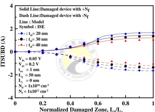
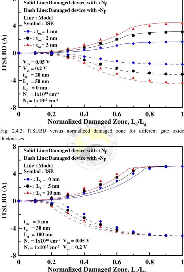
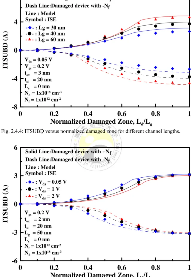
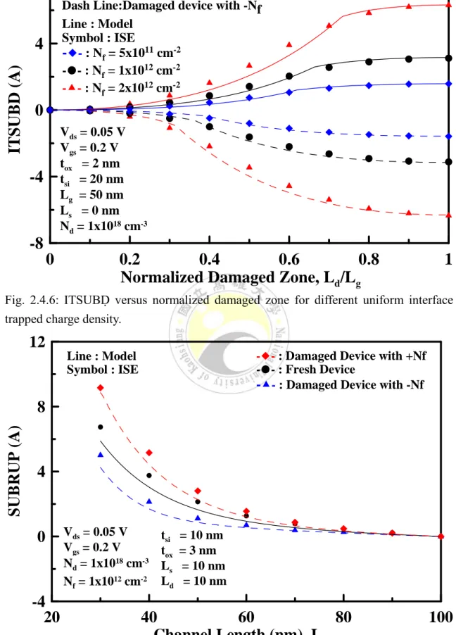
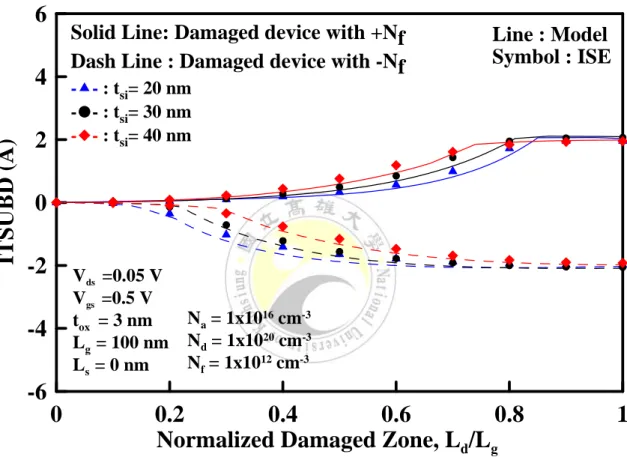
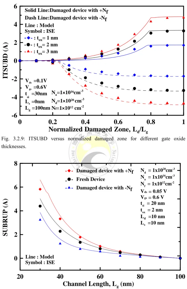
(26) 2.4 Results and Discussion We used the 3D device simulator "DESSIS" [28] to validate the proposed model. With the fixed positive/negative trapped charges, Fig. 2.4.1 plots ITSUBD versus normalized damaged zone Ld/Lg for different silicon film thicknesses. Increased the Ld/Lg can further enhance ITSUBD for both positive and negative trapped charges. A thick silicon film of tsi=40 nm is desirable for reducing the ITSUBD caused by the both positive and negative trapped charges. Fig. 2.4.2 shows ITSUBD with Ld/Lg for different gate oxide thicknesses. Irrespective of the polarities for the trapped charges, tox=1 nm induces a smaller ITSUBD than tox=2 nm and 3 nm. Although a thin gate oxide is needed to make the device suffer less ITSUBD, it may initiate the oxide leakage current due to the tunneling effects, which will cause the static power consumption. The trade-off regarding how to reduce ITSUBD without inducing the gate leakage current caused by the tunneling effects should be taken into account as the thin gate device is applied for memory circuits. Fig. 2.4.3 plots ITSUBD versus normalized damaged zone for different stressed lengths near the drain side. The ITSUBD is increased when Ls is increased, which implies that for the fixed channel length, the device will suffer severe ITSUBD when the damaged zone Ld keeps away from the drain side corresponding to the increased Ls. Fig. 2.4.4 plots ITSUBD versus normalized damaged zone for different channel lengths. Although the short-channel device shows worse immunity to shortchannel effects (SCEs), it suffers less ITSUBD caused by the ITCEs than the longchannel device when the normalized damaged zone is increased. On the contrary, the long-channel device suffers more ITSUBD caused by ITCEs than the short-channel device. Fig. 2.4.5 plots ITSUBD as a function of Ld/Lg for different drain voltages Vds. As opposed to SCEs, the larger Vds can reduce more ITCEs that improve the ITSUBD more efficiently than the smaller Vds. Although the enhanced SCEs in Fig. 2.4.1, Fig. 14.
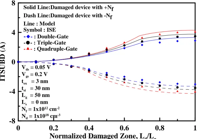
(27) 2.4.4, and Fig. 2.4.5 can alleviate ITSUBD more efficiently, the physical insight into the device physics is that when the SCEs are enhanced by the choice of device dimensions and drain voltage, the virtual cathode (i.e., the location of the leakiest path) will move toward the source side [29][30], which hence increases the distance between the damaged zone and the virtual cathode and the impact of the interface trapped charges (i.e., ITCEs) on the short-channel subthreshold current degradation (i.e., ITSUBD) can be expected to be reduced due to the enlarged distance from the virtual cathode to damaged zone. Fig. 2.4.6 plots ITSUBD versus normalized damaged zone for different trapped charge densities. The more trapped charge density the device has, the more ITSUBD the device will encounter. Fig. 2.4.7 plots subthreshold current roll-up versus the channel length for both damaged and fresh devices. The subthreshold current roll-up (SUBRUP) is defined by the difference between the long-channel and short-channel devices for their subthreshold currents in logarithm scales. (i.e., SUBRUP =Log[Ids,short]Log[Ids,long]). As the channel length is reduced, the damaged device with negative trapped charges suffers less short-channel effects (SCEs) and has a smaller SUBRUP than the fresh device. In contrast to the negative trapped charges, the positive trapped charges can enhance SCEs and cause the damaged device more SUBRUP than the fresh device when the channel length is further decreased. The ITSUBD versus Ld/Lg for the different device structures, including JLDG, JLTG, and JLQG transistors, is demonstrated in Fig. 2.4.8. It shows that the JLDG device can resist ITSUBD more efficiently than both JLQG and JLTG devices when Ld/Lg is increased. As opposed to SCEs, JLQG device rather than JLDG device will suffer severe ITSUBD induced by ITCEs. Being similar to Fig. 2.4.1, Fig. 2.4.4, and Fig. 2.4.5, since JLDG FET suffers more SCEs than both JLQG and JLTG FETs, it will be the best among the three FETs in resisting ITCEs that brings about the severe ITSUBD. Although the quantum mechanics effects (QMEs) are not included in the present model, the ITSUBD in the QM case 15.
(28) should be identical to it in the classical case because both damaged and fresh device experience the same QMEs.. 4. Solid Line:Damaged device with +Nf Dash Line:Damaged device with -Nf Line : Model Symbol : ISE. ITSUBD (A). 2. -&- : tsi= 20 nm -,- : tsi= 30 nm -2- : tsi= 40 nm. 0 Vds = 0.05 V Vgs = 0.2 V tox = 1 nm Lg = 50 nm Ls = 0 nm Nd = 1x1018 cm-3 Nf = 1x1012 cm-2. -2. -4 0. 0.2 0.4 0.6 0.8 Normalized Damaged Zone, Ld/Lg. 1. Fig. 2.4.1: ITSUBD versus normalized damaged zone for different silicon body thicknesses.. 16.
(29) 8. Solid Line:Damaged device with +Nf Dash Line:Damaged device with -Nf Line : Model Symbol : ISE. ITSUBD (A). 4. -&- : tox= 1 nm -,- : tox= 2 nm -2- : tox= 3 nm. 0 Vds = 0.05 V Vgs = 0.2 V tsi = 20 nm Lg = 50 nm Ls = 0 nm Nd = 1x1018 cm-3 Nf = 1x1012 cm-2. -4. -8 0. 0.2 0.4 0.6 0.8 Normalized Damaged Zone, Ld/Lg. 1. Fig. 2.4.2: ITSUBD versus normalized damaged zone for different gate oxide thicknesses.. 8. Solid Line:Damaged device with +Nf Dash Line:Damaged device with -Nf Line : Model Symbol : ISE. ITSUBD (A). 4. -&- : Ls = 0 nm -,- : Ls = 5 nm -2- : Ls = 10 nm. 0 tox = 3 nm tsi = 30 nm Lg = 100 nm Nd = 1x1018 cm-3 Vds = 0.05 V Nf = 1x1012 cm-2 Vgs = 0.2 V. -4. -8 0. 0.2 0.4 0.6 0.8 Normalized Damaged Zone, Ld/Lg. 1. Fig. 2.4.3: ITSUBD versus normalized damaged zone for different stressed near the drain side Ls. 17.
(30) 8. Solid Line:Damaged device with +Nf Dash Line:Damaged device with -Nf Line : Model Symbol : ISE. ITSUBD (A). 4. -&- : Lg = 30 nm -,- : Lg = 40 nm -2- : Lg = 60 nm. 0 Vds = 0.05 V Vgs = 0.2 V tox = 3 nm tsi = 20 nm Ls = 0 nm Nd = 1x1018 cm-3 Nf = 1x1012 cm-2. -4. -8 0. 0.2 0.4 0.6 0.8 Normalized Damaged Zone, Ld/Lg. 1. Fig. 2.4.4: ITSUBD versus normalized damaged zone for different channel lengths.. 6. Solid Line:Damaged device with +Nf Dash Line:Damaged device with -Nf Line : Model Symbol : ISE. ITSUBD (A). 3. -&- : Vds = 0.05 V -,- : Vds = 1 V -2- : Vds = 2 V. 0 Vgs = 0.2 V tox = 2 nm tsi = 20 nm Lg = 50 nm Ls = 0 nm Nf = 1x1012 cm-2 Nd = 1x1018 cm-3. -3. -6 0. 0.2 0.4 0.6 0.8 Normalized Damaged Zone, Ld/Lg. Fig. 2.4.5: ITSUBD versus normalized damaged zone for different drain bias.. 18. 1.
(31) 8. Solid Line:Damaged device with +Nf Dash Line:Damaged device with -Nf Line : Model Symbol : ISE -&- : Nf = 5x1011 cm-2 -,- : Nf = 1x1012 cm-2 -2- : Nf = 2x1012 cm-2. ITSUBD (A). 4. 0 Vds = 0.05 V Vgs = 0.2 V tox = 2 nm tsi = 20 nm Lg = 50 nm Ls = 0 nm Nd = 1x1018 cm-3. -4. -8 0. 0.2 0.4 0.6 0.8 Normalized Damaged Zone, Ld/Lg. 1. Fig. 2.4.6: ITSUBD versus normalized damaged zone for different uniform interface trapped charge density.. 12 -&- : Damaged Device with +Nf -,- : Fresh Device -2- : Damaged Device with -Nf. Line : Model Symbol : ISE. SUBRUP (A). 8. 4. 0. -4 20. Vds = 0.05 V Vgs = 0.2 V Nd = 1x1018 cm-3 Nf = 1x1012 cm-2. tsi tox Ls Ld. = 10 nm = 3 nm = 10 nm = 10 nm. 40 60 80 Channel Length (nm), Lg. Fig. 2.4.7: Subrup versus gate length for both fresh and damaged devices.. 19. 100.
(32) 8. Solid Line:Damaged device with +Nf Dash Line:Damaged device with -Nf Line : Model Symbol : ISE -&- : Double-Gate -,- : Triple-Gate -2- : Quadruple-Gate. ITSUBD (A). 4. 0. Vds = 0.05 V Vgs = 0.2 V tox = 3 nm tsi = 30 nm Lg = 50 nm Ls = 0 nm Nf = 1x1012 cm-2 Nd = 1x1018 cm-3. -4. -8 0. 0.2 0.4 0.6 0.8 Normalized Damaged Zone, Ld/Lg. 1. Fig. 2.4.8: ITSUBD versus normalized damaged zone for different device structures, including JLDG, JLTG, and JLQG MOSFETs.. 20.
(33) Chapter 3 TWO-DIMENSIONAL SUBTHRESHOLD BEHAVIOR MODEL FOR SURROUNDINGGATE MOSFETs WITH INTERFACE TRAPPED CHARGES 3.1 Quasi-2D Subthreshold Behavior Model for Surrounding-Gate MOSFETs with Interface Trapped Charges 3.1.1 Introduction ITRS has revealed that the implantations of non-classical CMOS structures are needed to overcome the difficult challenges when the semiconductor technology node is below 16 nm [1]. It also indicates that the multiple-gate (MG) MOSFETs with the strong field confinement, prominent volume conduction, and high packing density can be the promising candidates for the future CMOS application. Several literatures have reported that the novel structures for the surrounding-gate (SRG) MOSFETs with the high performance and scalability can be used for the memory DRAM cell [14]. To utilize this device for the memory cell application, it is mandatory to develop a feasible model. Although a numerous of literatures have modeled the drain current for the MG devices [31], [32], there are no investigations on the subthreshold current model for the surrounding-gate (SRG) MOSFETs with the interface trapped charges. In this letter, by accounting for the effects of interface trapped charges on the flatband voltage, we propose a compact subthreshold current model for the SRG MOSFETs with the 21.
(34) interface trapped charges based on the scaling equation and drift-diffusion approach. The proposed model explicitly illustrates how the interface trapped charges with different polarities, damaged zone lengths, gate oxide, and silicon body thicknesses affect the subthreshold current degradation. Hot-carrier effects that bring about the accumulated interface trapped charges will degrade the device/circuit performance [33], [3]. A number of literature works have modeled the hot-carrier-induced threshold voltage of planar and double-gate MOSFETs in the past decade [4], [5]. However, the wrong eigenvalue of k for the potential developed by the double-gate model [4] could mislead the device physics. Surroundinggate MOSFETs showing better scaling length are more promising than both planar and double-gate MOSFETs for future VLSI circuits. Until now, there have been few papers investigating the threshold-voltage model of surrounding-gate MOSFETs with trapped charges [34]. In this chapter, by considering the effects of equivalent oxide charges on flatband voltage [27], a compact analytical threshold-voltage model for surroundinggate MOSFETs with interface trapped charges is developed. The proposed model is verified by numerical simulation [28] and explicitly illustrates how trapped-charge density with different polarities, damaged zone, oxide thickness, and diameter of silicon body affect the threshold-voltage behavior. It not only offers physical insight into hotcarrier effects on threshold voltage but also provides basic design guidance for chargetrapped memory devices.. 22.
(35) 3.1.2 Model Description Fig. 3.1.1 shows the 3D device structure to derive the model. With various interface trapped-charge distributions, the channel regions can be divided into three zones, region 1, 2, and 3 signify the low-field region near the source, the high-field region with damage, and the high-field region without damage, respectively.. Fig. 3.1.1: Typical schematic of the 3D SRG device structure. Regions 1, 3, and 2 are defined by region 1: fresh region at the interface of Si/SiO2 near the source side when 0 ≦z≦Lg-Ld-Ls, region 2: damaged region at the interface of Si/SiO2 when Lg-Ld-Ls≦z ≦Lg- Ls, and region 3: fresh region at the interface of Si/SiO2 near the drain side when Lg-Ls≦z≦Lg. Lg is the channel length, Ld is the damaged zone, Ls is the fresh zone near the drain side, and Lg-Ld-Ls is the fresh zone near the source side. 23.
(36) 3.1.3 Threshold Voltage Model Derivation With various interface trapped-charge distributions, the channel regions can be divided into three zones. By considering the central conduction mode and using the parabolic approach to solve for the 2D Poisson equation in each of the three zones, the potential along the vertical channel direction can be assumed [37] Φi(r, z) = C1,i(z) + C2,i(z)r + C3,i(z)r2 (i = 1, 2, and 3 signify the low-field region near the source, the highfield region with damage, and the high-field region without damage, respectively) to satisfy the following conditions: Φ i (0, z ) = C1,i ( z ) = Φ C ,i ( z ) ∂Φ i (r , z ) ∂r ∂Φ i (r , z ) ∂r. 1 r = tsi 2. r =0. = Cox. Vgs − V fb − Φ S ,i ( z ). ε si. (3.1.1). =0. Where Φc,i(z) is the central potential, Φs,i(z) is the surface potential, COX is the effective capacitance per unit area [37], and Vfb,1 = Vfb,3 is the flatband voltage in the undamaged regions. In the damaged region, due to the effect of equivalent oxide charges on flatband voltage [27], we obtain V fb ,2 = V fb ,1 −. qN f 1 tox x ρ ( x) dx + Qit ] = V fb ,1 − [∫ 0 Cox tox Cox. (3.1.2). Where ρ(x) is the localized oxide charge density assumed to be zero for simplicity and Qit = qNf is the uniform interface charge sheet density. With the determined C1,i, C2,i, and C3,i from (3.1.1) and by setting r = 0 for the central conduction channel, the central potential Φc,i(z) should satisfy d 2 Φ C ,i ( z ) dz 2. −. 1. λSRG 2. (Φ C ,i ( z ) − φC ,i ) = 0. with. 24. (3.1.3).
(37) λSRG 2 =. 4tsi ε si + Cox tsi 2 16Cox. φC ,i = Vgs - V fb,i −. qN a. ε si. (3.1.4). λSRG 2. (3.1.5). Where the subscript of i =1, 3 denotes the fresh region and i=2 denotes the damaged region, Cox is effective oxide capacitance per unit area, Vgs is the gate bias, λSRG and φC,i are the scaling length and long-channel central potential, respectively, and Vfb,1=Vfb,3 is the flat-band voltage in the fresh region. By solving for the ordinary differential equation, the general solution of (3.1.3) can be obtained as z. Φ C ,i ( z ) = ai e. λSRG. + bi e. −. z. λSRG. + φC ,i. (3.1.6). According to the continuity of both electric field and potential at the boundary conditions at damaged/fresh regions, source/silicon and drain/silicon junctions, ai and bi in (3.1.6) can be obtained as a1 =. coth (kLg ) -1. [(cosh (kL1 - kLg ) - cosh (kL2 - kLg )) 2 kL (φC ,2 - φC ,1 ) + Vds + Vbi - φC ,1 )e g - Vbi + φC ,1 ]. b1 =. csch(kLg ). [( cosh (kL2 − kLg ) − cosh (kL1 − kLg )) 2 kL (φC ,2 − φC ,1 ) + e g (Vbi − φC ,1 ) − Vbi − Vds + φC ,3 ]. a2 =. b2 =. coth(kLg ) −1 2 −. qN f. −. e. Cox. [e g (Vbi + Vds − φC,2 + kL. qN f Cox. −Vbi + (φC,2 − φC,1 )(cosh(kL1 ) −. ) + φC,2. ekL2 2. 2. (3.1.9). )]. 2 kL. [2e g Vbi − 2e g (Vbi + Vds ) 4 k (L + 2 L ) k (2 L − L ) + (φC ,1 − φC ,2 )(e 1 g − ekL2 + e g 1. a3 =. (3.1.8). k (2 Lg − L2 ). coth (kLg ) − 1. −e. (3.1.7). k (2 Lg − L2 ). kL. ) − 2(φC ,2 −. coth (kLg ) − 1. qN f Cox. )(e. 2 kLg. − e g )] kL. [e g (Vbi + Vds − φC ,3 ) + φC ,1 − Vbi 2 + (φC ,2 − φC ,1 )( cosh (kL1 ) − cosh (kL2 ))] kL. 25. (3.1.10). (3.1.11).
(38) b3 =. e. kLg. ( coth (kLg ) − 1) 2. + φC ,1 + e. kLg. [e. kLg. (Vbi − φC ,1 ) − Vbi − Vds. (3.1.12). (φC ,2 − φC ,1 )( cosh (kL2 ) − cosh (kL1 ))]. k=1/λSRG, L1=Lg-Ld-Ls, and L2=Lg-Ls,φC,I (i=1,2, and 3) is the long-channel central potential in both fresh and damaged regions, respectively. Therefore, the minimum central potential can be expressed as Φ C ,i ,min = 2 ai bi + φC ,i. (3.1.13). By setting Φc,i,min = 2ΦB and solving for the Vgs in (3.1.13), we can obtain the threshold voltage VTH ,i = V fb,i −. 2 qN a tsi Bi + Bi − Ai Ci − 4COX Ai. (3.1.14). where. Bi = −2 ( Φ B + βi γ i + αiηi ). (3.1.15) (3.1.16). Ci = 4(Φ B 2 − βiηi ). (3.1.17). Ai = 1 − 4α i γ i. α1 = α 2 = α3 =. β1 =. coth (kLg ) − 1 2. (1 − e. kLg. (3.1.18). ). coth(kLg ) −1 [((cosh(kL1 − kLg ) − cosh(kL2 − kLg )) 2 kL (φC,2 −φC,1 ) +Vds +Vbi )e g −Vbi ]. β2 =. coth(kLg ) − 1 2. [e. kLg. (Vbi + Vds +. qN f Cox. )−. qN f Cox. − Vbi. k (2 L − L2 ). ekL2 e g + (φC ,2 − φC ,1 )(cosh(kL1 ) − − 2 2. β3 =. coth (kLg ) − 1. γ2 = γ3 =. kL. csc h(kLg ) 2. (1 − e. coth (kLg ) − 1 2. 26. (e. kLg. kLg. (3.1.21). (3.1.22). ). −e. (3.1.20). )]. [e g (Vbi + Vds ) − Vbi 2 + (φC ,2 − φC ,1 )( cosh (kL1 ) − cosh (kL2 ))]. γ1 =. (3.1.19). 2 kLg. ). (3.1.23).
(39) η1 =. η2 =. csch (kLg ). [( cosh (k (L2 − Lg )) − cosh (k (L1 − Lg ))) 2 (φC ,2 − φC ,1 ) + (ekLg − 1)Vbi − Vds ]. (3.1.24). coth (kLg ) − 1 2qN f 2 kLg kL [ (e −e g ) 4 Cox + (φC ,1 − φC ,2 )(e − 2e. kLg. k (L1 + 2 Lg ). (Vbi + Vds ) + 2e. − e kL2 + e. 2 kLg. e g ( coth (kLg ) − 1). k (2 Lg − L1 ). −e. k (2 Lg − L2 ). ). (3.1.25). Vbi ]. kL. η3 =. 2 +e. kLg. [(e. kLg. − 1)Vbi − Vds. (3.1.26). (φC ,2 − φC ,1 )( cosh (kL2 ) − cosh (kL1 ))]. Vbi is the built-in voltage at the source/channel and drain/channel junctions and Vds is the drain voltage. The largest value of VTH,i in (3.1.14) will dominate the threshold voltage behavior.. 27.
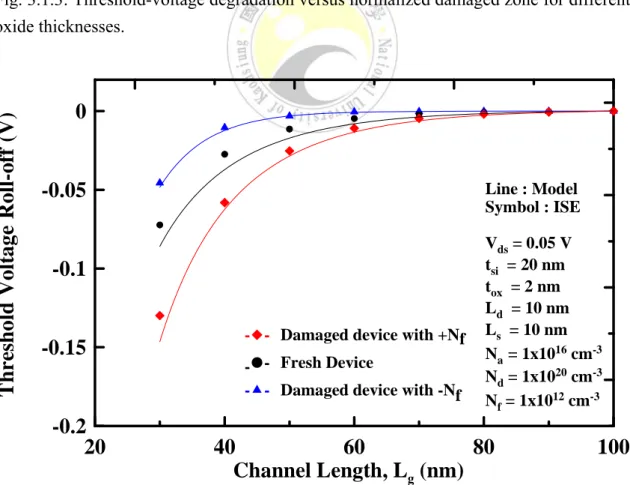
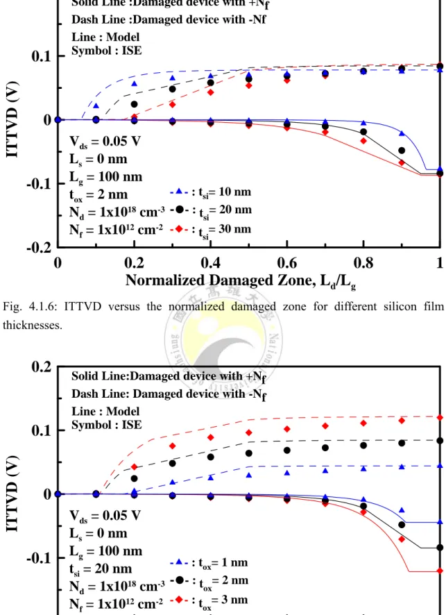
(40) 3.1.4 Threshold Voltage Model Result The 3D device simulator “DESSIS” is used to verify the proposed model. The threshold voltage is read when the electron concentration at the position of the minimum central potential is equal to the bulk doping density. For the fixed positive/negative interface sheet charge density, Fig. 3.1.2 shows the dependence of threshold-voltage degradation on the normalized damaged zone for different diameters of silicon body. The increased damaged zone can further degrade the threshold voltage by reflecting the effects of negative/positive interface trapped charges on the weakening/strengthening DIBL from the lateral electric field of the drain side. This interface-trapped-charge-induced threshold-voltage degradation is called “ITTVD.” For positive interface charges, the small diameter of silicon body of tsi = 10 nm will suffer less ITTVD in comparison to the large diameter of tsi = 30 nm when Ld is increased. However, the small diameter of tsi = 10 nm with negative interface charges will not suffer more ITTVD than the large diameter of tsi = 30 nm until the normalized damaged zone of Ld/Lg is shrunk approximately below 0.55. Fig. 3.1.3 shows the variation of threshold-voltage degradation with the normalized damaged zone for different oxide thicknesses. Positive/negative interface charges with large damaged zone will bring about great threshold-voltage degradation, particularly for thick oxide thickness. To make the device suffer less ITTVD, not only the thin gate oxide should be accounted for but also the small damaged zone must be desired for the device. Fig. 3.1.4 shows the dependence of threshold-voltage roll-off on channel length for both damaged and fresh devices. The device with negative charges suffers less SCEs than the fresh device due to screening DIBL, which hence reduces the threshold-voltage roll-off. On the other hand, positive charges can enhance DIBL that will induce severe 28.
(41) ITTVD and cause the damaged device more threshold-voltage roll-off than the fresh device.. 0.16. Solid Line :Damaged device with +Nf Dash Line :Damaged device with -Nf Line : Model Symbol : ISE. ITTVD (V). 0.08. -2- : tsi = 10 nm -,- : tsi = 20 nm -&- : tsi = 30 nm. 0 Vds = 0.05 V Ls = 0 nm Lg = 50 nm tox = 2 nm. -0.08. Nd = 1x1020 cm-3 Na = 1x1016 cm-3 Nf = 1x1012 cm-2. -0.16 0. 0.2 0.4 0.6 0.8 Normalized Damaged Zone, Ld/Lg. 1. Fig. 3.1.2: Threshold-voltage degradation versus normalized damaged zone for different diameters of silicon body. 29.
(42) 0.2. Solid Line:Damaged device with +Nf Dash Line: Damaged device with -Nf Line : Model Symbol : ISE. ITTVD (V). 0.1. -2- : tox= 2 nm -,- : t = 3 nm. 0. ox. -&- : t = 4 nm ox. Vds = 0.05 V Ls = 0 nm Lg = 50 nm tsi = 20 nm. -0.1. Nd = 1x1020 cm-3 Na = 1x1016 cm-3 Nf = 1x1012 cm-2. -0.2 0. 0.2 0.4 0.6 0.8 Normalized Damaged Zone, Ld/Lg. 1. Threshold Voltage Roll-off (V). Fig. 3.1.3: Threshold-voltage degradation versus normalized damaged zone for different oxide thicknesses.. 0. -0.05. Line : Model Symbol : ISE. -0.1. -0.15. -0.2 20. -&- Damaged device with +Nf -,- Fresh Device -2- Damaged device with -Nf. Vds = 0.05 V tsi = 20 nm tox = 2 nm Ld = 10 nm Ls = 10 nm Na = 1x1016 cm-3 Nd = 1x1020 cm-3 Nf = 1x1012 cm-3. 40 60 80 Channel Length, Lg (nm). 100. Fig. 3.1.4: Threshold-voltage roll-off versus channel length for both fresh and damaged devices. 30.
(43) 3.1.5 Subthreshold Current Model Derivation For various trapped charge distributions, the channel can be divided into three regions as shown in Fig. 3.1.1. In the subthreshold regime, the channel central potential should satisfy the following scaling equation [35]: d 2 Φ C ,i ( z ) dz. 2. −. 1. λSRG 2. (Φ C ,i ( z ) − φC ,i ) = 0. (3.1.27). with λSRG 2 =. 4tsi ε si + Cox tsi 2 16Cox. φC ,i = Vgs - V fb,i −. qN a. ε si. (3.1.28). λSRG 2. (3.1.29). Where the subscript of i =1, 3 denotes the fresh region and i=2 denotes the damaged region, Cox is effective oxide capacitance per unit area, Vgs is the gate bias, λSRG and φC,i are the scaling length and long-channel central potential, respectively, and Vfb,1=Vfb,3 is the flat-band voltage in the fresh region. Due to the effect of equivalent oxide charges on the flat-band voltage, the flat-band voltage in the damaged region can be expressed by [27]: V fb ,2 = V fb ,1 −. qN f Qit = V fb ,1 − Cox Cox. (3.1.30). Where Qit= qNf is the interface trapped charge density that is assumed uniform for simplicity. The general solution of (3.1.27) is z. Φ C ,i ( z )=ai e. λSRG. + bi e. −. z. λSRG. + φC , i. (3.1.31). According to the continuity of both electric field and potential at the boundary conditions at damaged/fresh regions, source/silicon and drain/silicon junctions, ai and bi in (3.1.31) can be obtained as. 31.
數據
+7

相關文件
雖然水是電中性分子,然其具正極區域(氫 原子)和負極區域(氧原子),因此 水是一種極 性溶劑
細目之砂紙,將絕緣體 及內部半導電層鉛筆狀
Z 指令 ping 為重要的使用 ICMP 封包的指令. Z 若設定防火牆,並非所有的 ICMP
◦ 金屬介電層 (inter-metal dielectric, IMD) 是介於兩 個金屬層中間,就像兩個導電的金屬或是兩條鄰 近的金屬線之間的絕緣薄膜,並以階梯覆蓋 (step
• Follow Example 21.5 to calculate the magnitude of the electric field of a single point charge.. Electric-field vector of a
雙極性接面電晶體(bipolar junction transistor, BJT) 場效電晶體(field effect transistor, FET).
Biases in Pricing Continuously Monitored Options with Monte Carlo (continued).. • If all of the sampled prices are below the barrier, this sample path pays max(S(t n ) −
• P u is the price of the i-period zero-coupon bond one period from now if the short rate makes an up move. • P d is the price of the i-period zero-coupon bond one period from now
