超寬頻無線網路應用之低功率高速類比數位轉換器設計
112
0
0
全文
(2) 超寬頻無線網路應用之 低功率高速類比數位轉換器設計 A Low-Power High-Speed A/D Converter Design for UWB Wireless Applications 研 究 生:陳世基. Student:Shih-Chi Chen. 指導教授:溫瓌岸 博士. Advisor:Dr. Kuei-Ann Wen. 國 立 交 通 大 學 電機學院 電子與光電學程 碩 士 論 文. A Thesis Submitted to College of Electrical and Computer Engineering National Chiao Tung University in Partial Fulfillment of the Requirements for the Degree of Master of Science in Electronics and Electro-Optical Engineering. June 2007 Hsinchu, Taiwan, Republic of China. 中華民國九十六年六月. II.
(3) 超寬頻無線網路應用之 低功率高速類比數位轉換器設計 學生:陳世基. 指導教授:溫瓌岸 博士. 國 立 交 通 大 學 電機學院. 電子與光電學程碩士班. 摘. 要. 本篇論文提出利用互補金氧半製程實現一應用於極寬頻無線通訊系統的六位元、每 秒 20 億次、寬頻低功率的快閃式類比數位轉換器。提出一結合串級電阻平均技術、內 差技術、取樣保持電路和數位錯誤校正技術的低功率高速架構。對於平均技術、內差技 術、取樣保持電路和數位校正技術的原理有詳細的分析和討論。使用平均技術,可以減 少前級放大器的功率消耗。使用內差技術,可以使前級放大器的數量和輸入電容減半。 使用取樣保持電路,可以改善動態效能。使用數位校正技術可以減少 2N-1 個管線式閂鎖 的功率。結合這些技術,在輸入頻率高達 976 百萬赫茲,每秒 20 億次取樣的情況下, 六位元快閃式類比數位轉換器可實現 5.05 的有效位元。在微分非線性度和積分非線性 度的結果分別低於 0.1LSB和 0.14LSB。信號對雜訊失真比和無雜波干擾之動態範圍在信 號為 7.81 百萬赫茲時分別為 37.51 分貝和 48.94 分貝。信號對雜訊失真比和無雜波干 擾之動態範圍在信號為接近Nyquiest頻率時分別為 32.2 分貝和 33.68 分貝。整個類比 數位轉換器的消耗功率在 1.2 伏特的電壓下消耗 117 毫瓦,FOM只有 1.8p焦耳。 此快閃式類比數位轉換器是使用聯電 0.13 微米單層複晶矽 8 層金屬互補金氧半製 程來實現,採用矽品 QFN32 來包裝並且黏著在印刷電路板上以利於測量。信號對雜訊失. I.
(4) 真比在 20 億赫茲的取樣頻率以及輸入信號為 2.00 百萬赫茲時的量測結果為 27.97 分 貝。計算出的有效位元為 4.3 位元。所量測到的微分非線性度和積分非線性度為 +1.56/-1.00 LSB 和 +1.91/-1.85 LSB。. II.
(5) A Low-Power High-Speed A/D Converter Design for UWB Wireless Applications Student:Shih-Chi Chen. Advisor:Dr. Kuei-Ann Wen. Degree Program of Electrical and Computer Engineering National Chiao Tung University. ABSTRACT A 6-bit 2-GSample/s flash A/D converter with wide bandwidth and low power for ultra-wideband (UWB) application is demonstrated in CMOS technology. A low-power high-speed architecture by combining the cascade resistive averaging, interpolation, wideband sample-and-hold and digital error correction technique is proposed. The principle of averaging, interpolation, wideband sample-and- hold technique and digital error correction is analyzed and discussed in detail. Use the averaging, can reduce power in preamplifiers. Use the interpolation can halve the number of preamplifiers and halve input capacitance. Use the sample-and-hold can improve dynamic performance. Use the digital error correction to can eliminate the power of 2N-1 pipeline latches. With the combining techniques, a 6-bits flash A/D converter achieves effective 5.05 bits for input frequencies up to 976MHz at 2-GSample/s. The results show peak differential-nonlinearity (DNL) and integral-nonlinearity (INL) is less than 0.1LSB and 0.14LSB. The signal-to-noise and distortion ratio (SNDR) at. III.
(6) 7.81MHz is 37.51dB and the spurious-free dynamic range (SFDR) at 7.81MHz is 48.94dB. Near Nyquiest input frequencies, SNDR and SFDR maintain above 32.2 and 33.68dB respectively. This flash A/D converter consumes 117mW from 1.2V power supply at 2-GSample/s, and a figure of merit (FOM) is only 1.8pJ. The flash A/D converter is implemented in UMC 0.13μm 1P8M CMOS technology and has been packaged in SPIL QFN32 which is mounted on PCB board in favor of measurement. The measurement of the SNDR is 27.97dB under 2GHz sampling rate and 2.00MHz input frequency. The effective number of bits (ENOB) is calculated equal to 4.3 bits. The measured DNL and INL are +1.56/-1.00 LSB and +1.91/-1.85 LSB.. IV.
(7) 誌. 謝. 在碩士研究生涯中,首要致謝的是 TWT 實驗室的指導教授-溫瓌岸博士,賦予了優 渥的環境及不間斷地授予國內外的新知,使我增廣見聞,獲益良深。並感謝溫文燊博士, 專業地指導與不吝的賜教,使得研究更臻完美。此外,感謝另兩位口試委員-高耀煌教 授,中正大學張盛富教授,給予了豐富、寶貴的建議。. 感謝實驗室的四位學長-陳哲生學長、趙皓名學長、鄒文安學長、林立協學長,在 研究的過程,適時地提供協助與意見,裨益研究不少。再者,感謝實驗室的同儕-顯聰、 聰明、建龍、家岱、漢健、閎仁、書旗、振威、昱瑞、建毓,在學業及生活上彼此切磋 砥勵,互助合作。亦感謝實驗室的學弟們-磊中、佳欣、俊彥、國爵、謙若、士賢、柏 麟、為實驗室營造了歡欣的氣氛,緩和舒解掉不少緊張與壓力。更感謝助理們的幫助, 排除萬難,令研究進展順遂。. 最後,感謝這一路走來始終在背後默默支持陪伴我的家人及朋友,無怨無悔的關愛 和付出,在研究遭逢瓶頸,為沮喪失落之枷鎖所羈絆之際,為我身心靈帶來了莫大的鼓 舞與安慰,培養鍥而不捨,愈挫愈勇之向上精神。. 本論文獻給所有關懷、摯愛我的人,今有此成就得功歸於你們,畢業後,定當秉持 著恭敬謙遜之情,發揮自我專業,貢獻國家,服務並回饋社會人群。. 誌于. 2007. 陳世基. V.
(8) Contents 摘. 要..................................................................................................................................................................I. ABSTRACT ........................................................................................................................................................ III 誌. 謝.................................................................................................................................................................. V. CONTENTS.........................................................................................................................................................VI. LIST OF FIGURES.............................................................................................................................................IX. LIST OF TABLES............................................................................................................................................XIII. CHAPTER 1 INTRODUCTION....................................................................................................................... 1 1.1 MOTIVATION ................................................................................................................................................. 3 1.2 THESIS ORGANIZATION ................................................................................................................................. 4 CHAPTER 2 REVIEW OF A/D CONVERTER ARCHITECTURES AND APPLICATIONS ................. 5 2.1 A/D CONVERTER ARCHITECTURES ................................................................................................................ 5 2.1.1 Flash A/D Converter ............................................................................................................................. 6 2.1.2 Pipelined A/D Converter....................................................................................................................... 8 2.1.3 Sigma-Delta A/D Converter.................................................................................................................. 9 2.1.4 Summary of A/D converter Architectures .......................................................................................... 10 2.2 A/D CONVERTER APPLICATIONS .................................................................................................................. 12 2.2.1 Fiber-optic Communication ................................................................................................................ 12 2.2.2 Digital Oscilloscope............................................................................................................................ 13 2.2.3 Medical Imaging ................................................................................................................................. 14 2.2.4 CCD Imaging Electronics ................................................................................................................... 14 2.2.5 Touchscreen Digitizers ....................................................................................................................... 15 2.2.6 Digital Audio ...................................................................................................................................... 16 CHAPTER 3 LOW-POWER HIGH-SPEED TECHNIQUES AND CIRCUIT DESIGN ......................... 18 3.1 SAMPLE-AND-HOLD TECHNIQUE ................................................................................................................. 19 VI.
(9) 3.2 INTERPOLATION TECHNIQUE ....................................................................................................................... 24 3.3 AVERAGING TECHNIQUE ............................................................................................................................. 26 3.3.1 Spatial Filtering of the Averaging Resistive Network ........................................................................ 27 3.3.2 Error Correction Factor (ECF)............................................................................................................ 30 3.3.3 Nonlinearity Error and Compensation at the Edges............................................................................ 33 3.3.4 Power Saving in Preamplifiers Array ................................................................................................. 37 3.4 DIGITAL ERROR CORRECTION TECHNIQUE .................................................................................................. 39 3.4.1 Bubble Error Correction...................................................................................................................... 39 3.4.2 Metastability Error Correction ............................................................................................................ 40 3.5 RESISTOR LADDER DESIGN.......................................................................................................................... 46 3.6 PREAMPLIFIER DESIGN ................................................................................................................................ 48 3.7 COMPARATOR DESIGN ................................................................................................................................. 51 3.8 DIGITAL LOGIC DESIGN ............................................................................................................................... 53 3.9 CLOCK GENERATOR DESIGN ....................................................................................................................... 55 3.10 SIMULATION RESULTS ............................................................................................................................... 57 3.10.1 Static Performance Simulation.......................................................................................................... 57 3.10.2 Dynamic Performance Simulation .................................................................................................... 59 CHAPTER 4 EXPERIMENT RESULTS ...................................................................................................... 65 4.1 LAYOUT DESIGN CONSIDERATION ............................................................................................................... 65 4.2 ESD PROTECTION AND PACKAGE ................................................................................................................ 67 4.3 PRINTED CIRCUIT BOARD (PCB) DESIGN .................................................................................................... 70 4.4 MEASUREMENT SETUP ................................................................................................................................ 74 4.5 MEASUREMENT RESULTS ............................................................................................................................ 76 4.5.1 Dynamic Testing................................................................................................................................. 76 4.5.1.1 Sampling Frequency at 300MHz ...................................................................................................................78 4.5.1.2 Sampling Frequency at 2GHz........................................................................................................................81. 4.5.2 Static Testing ...................................................................................................................................... 83 4.6 SUMMARY ................................................................................................................................................... 85 CHAPTER 5 CONCLUSIONS ....................................................................................................................... 86 5.1 SUMMARY ................................................................................................................................................... 86 VII.
(10) 5.2 FUTURE WORK ............................................................................................................................................ 87 BIBLIOGRAPHY ............................................................................................................................................... 88. APPENDIX .......................................................................................................................................................... 91 簡. 歷............................................................................................................................................................... 97. VIII.
(11) List of Figures FIGURE 1. 1 THE MULTI-BAND OFDM FREQUENCY BAND PLAN ........................................................................... 2 FIGURE 1. 2 THE DIRECT CONVERSION ARCHITECTURE FOR UWB RECEIVER ......................................................... 3 FIGURE 2. 1 FLASH A/D CONVERTER ARCHITECTURE ........................................................................................... 7 FIGURE 2. 2 PIPELINED A/D CONVERTER ARCHITECTURE ..................................................................................... 8 FIGURE 2. 3 SIGMA-DELTA A/D CONVERTER ARCHITECTURE ............................................................................. 10 FIGURE 2. 4 FIBER-OPTIC COMMUNICATION ........................................................................................................ 12 FIGURE 2. 5 DIGITAL OSCILLOSCOPE ................................................................................................................... 13 FIGURE 2. 6 DIGITAL RADIOGRAPHY SYSTEM...................................................................................................... 14 FIGURE 2. 7 GENERIC IMAGING SYSTEM FOR SCANNERS OR DIGITAL CAMERAS ................................................. 15 FIGURE 2. 8 FOUR-WIRE RESISTIVE TOUCHSCREEN INTERFACE .......................................................................... 16 FIGURE 2. 9 MODERN CELL PHONE HANDSET BLOCK .......................................................................................... 17 FIGURE 3. 1 BLOCK DIAGRAM OF THE PROPOSED LOW POWER A/D CONVERTER .................................................. 19 FIGURE 3. 2 BASIC S/H CONFIGURATION ............................................................................................................. 20 FIGURE 3. 3 PSEUDO-DIFFERENTIAL TYPE S/H CONFIGURATION ........................................................................ 21 FIGURE 3. 4 THE FIRST CROSS-COUPLING TYPE S/H CONFIGURATION WITH A PMOS LOADING .......................... 21 FIGURE 3. 5 THE SECOND CROSS-COUPLING TYPE S/H CONFIGURATION WITH A PMOS LOADING ...................... 22 FIGURE 3. 6 THE SIMULATION OF THE FIRST AND SECOND TYPE S/H.................................................................... 23 FIGURE 3. 7 INTERPOLATION PREAMPLIFIER ARCHITECTURE .............................................................................. 24 FIGURE 3. 8 GOOD ZERO CROSSING ..................................................................................................................... 25 FIGURE 3. 9 NO GAIN ERROR AT ZERO CROSSING ............................................................................................... 26 FIGURE 3. 10 RESISTIVE AVERAGING SCHEME AND ZERO CROSSING .................................................................. 27 FIGURE 3. 11 THE IMPULSE RESPONSE OF A RESISTOR NETWORK AS SPATIAL FILTER .......................................... 28 FIGURE 3. 12 IMPULSE RESPONSE AS A FUNCTION OF RESISTIVE RATIO R1/R0 AT NODE(0) ................................. 29 FIGURE 3. 13 THE ERROR CORRECTION FACTOR VERSE RESISTIVE AVERAGING RATIO ......................................... 31 FIGURE 3. 14 GAIN LOSS VERSE RESISTIVE AVERAGING RATIO ............................................................................ 32 FIGURE 3. 15 MONTE-CARLO SIMULATION SETUP SCHEME .................................................................................. 32 FIGURE 3. 16 THE PREAMPLIFIER MONTE-CARLO ANALYSIS WITH AND WITHOUT AVERAGING RESISTOR ........... 33 FIGURE 3. 17 DUMMY PREAMPLIFIERS TO REDUCE EDGE EFFECTS ....................................................................... 34 FIGURE 3. 18 THE CURRENT FLOWING IN RESISTIVE NETWORK SHOWS THE BOUNDARY CONDITION .................... 35 IX.
(12) FIGURE 3. 19 DUMMY PREAMPLIFIERS WITH CROSS CONNECTION AVERAGING .................................................... 35 FIGURE 3. 20 IMPULSE RESPONSE AS A FUNCTION OF RESISTIVE RATIO R1/R0=0.16 AT NODE(0) ........................ 36 FIGURE 3. 21 AVERAGING CURRENT FOLLOWING IN THE LOAD RESISTANCE ........................................................ 37 FIGURE 3. 22 THREE INPUT AND GATE TO SOLVE A BUBBLE ERROR .................................................................... 40 FIGURE 3. 23 FLASH A/D CONVERTER WITH COMPARATOR PIPELINING TO REDUCE METASTABILITY .................. 42 FIGURE 3. 24 ERROR PROPAGATION IN BINARY-ENCODED ROM AND OUTPUT BITS ............................................. 43 FIGURE 3. 25 SINGLE BIT ERROR IN ROM OUTPUT WITH THE AUXILIARY CIRCUITS AND GRAY-ENCODE ROM ... 44 FIGURE 3. 26 IMPLEMENTATION OF THE AUXILIARY CIRCUIT ............................................................................... 45 FIGURE 3. 27 SIMULATION RESULT OF THE AUXILIARY CIRCUIT AT 2GHZ OPERATION ........................................ 45 FIGURE 3. 28 CALCULATION MODEL TO DERIVE THE MAXIMUM LADDER IMPEDANCE ......................................... 47 FIGURE 3. 29 THE WIDEBAND PREAMPLIFIER SCHEMATIC .................................................................................... 48 FIGURE 3. 30 THE NONLINEAR MODEL OF A LIMITING PREAMPLIFIER STAGE........................................................ 49 FIGURE 3. 31 THIRD-ORDER DISTORTION VERSUS BANDWIDTH/INPUT FREQUENCY ............................................. 50 FIGURE 3. 32 THE SIMULATION OF THE WIDE BANDWIDTH PREAMPLIFIER ........................................................... 50 FIGURE 3. 33 LOW KICK BACK COMPARATOR SCHEMATIC ................................................................................... 51 FIGURE 3. 34 COMPARATOR OVERDRIVE TEST ..................................................................................................... 52 FIGURE 3. 35 THE SCHEMATIC OF TRUE SINGLE PHASE CLOCK FLIP-FLOP............................................................. 53 FIGURE 3. 36 GRAY-TO-BINARY DECODER WITH DELAY CIRCUITS ...................................................................... 54 FIGURE 3. 37 CLOCK GENERATOR WITH TRANSMISSION GATE AND CMOS LATCHES .......................................... 56 FIGURE 3. 38 THE SIMULATION OF THE CLOCK GENERATOR................................................................................. 56 FIGURE 3. 39 DNL AND INL SIMULATION OF FIRST VERSION A/D CONVERTER ................................................... 58 FIGURE 3. 40 DNL AND INL SIMULATION OF SECOND VERSION A/D CONVERTER ............................................... 58 FIGURE 3. 41 DYNAMIC PERFORMANCE AT A INPUT FREQUENCY OF 2MHZ FOR FIRST VERSION A/D CONVERTER, SAMPLED AT 2GHZ ......................................................................................................................... 59. FIGURE 3. 42 SNDR AND SFDR VERSUS INPUT FREQUENCY FOR FIRST VERSION A/D CONVERTER, SAMPLED AT 2GHZ .............................................................................................................................................. 60 FIGURE 3. 43 DYNAMIC PERFORMANCE AT A INPUT FREQUENCY OF 7.81MHZ FOR SECOND VERSION A/D CONVERTER, SAMPLED AT 2GHZ .................................................................................................... 61. FIGURE 3. 44 DYNAMIC PERFORMANCE AT A INPUT FREQUENCY OF 492.18MHZ FOR SECOND VERSION A/D CONVERTER, SAMPLED AT 2GHZ .................................................................................................... 61. X.
(13) FIGURE 3. 45 DYNAMIC PERFORMANCE AT A INPUT FREQUENCY OF 976.52MHZ FOR SECOND VERSION A/D CONVERTER, SAMPLED AT 2GHZ .................................................................................................... 62. FIGURE 3. 46 SNDR AND SFDR VERSUS INPUT FREQUENCY FOR SECOND VERSION A/D CONVERTER, SAMPLED AT 2GHZ .............................................................................................................................................. 62 FIGURE 3. 47 THE FOM COMPARISON WITH PUBLICATION PAPER ........................................................................ 64 FIGURE 4. 1 LAYOUT FLOORPLAN OF A/D CONVERTER ........................................................................................ 66 FIGURE 4. 2 CORE LAYOUT PHOTOGRAPH OF THE A/D CONVERTER ..................................................................... 67 FIGURE 4. 3 ESD PROTECTION CIRCUIT................................................................................................................ 68 FIGURE 4. 4 PACKAGE MODEL .............................................................................................................................. 68 FIGURE 4. 5 LAYOUT PHOTOGRAPH OF THE A/D CONVERTER .............................................................................. 69 FIGURE 4. 6 THE SCHEMATIC OF THE PIN ASSIGNMENT ........................................................................................ 70 FIGURE 4. 7 THE SCHEMATIC OF THE PCB DESIGN............................................................................................... 72 FIGURE 4. 8 THE LAYOUT OF THE PCB................................................................................................................. 72 FIGURE 4. 9 THE PCB OF THE FLASH A/D CONVERTER ........................................................................................ 73 FIGURE 4. 10 MEASUREMENT PLAN ..................................................................................................................... 74 FIGURE 4. 11 TRANSFORMER AND BIAS-T ........................................................................................................... 74 FIGURE 4. 12 TESTING ENVIRONMENT ................................................................................................................. 75 FIGURE 4. 13 DEVICE UNDER TEST ....................................................................................................................... 75 FIGURE 4. 14 DYNAMIC TESTING PLOT FROM LOGIC ANALYZER ......................................................................... 77 FIGURE 4. 15 DYNAMIC PERFORMANCE VERSUS SAMPLING FREQUENCY ............................................................. 77 FIGURE 4. 16 FFT PLOT AT 1.007MHZ INPUT FREQUENCY................................................................................... 78 FIGURE 4. 17 SNDR VERSUS INPUT FREQUENCY AT 300MHZ SAMPLING RATE ................................................... 79 FIGURE 4. 18 SFDR VERSUS INPUT FREQUENCY AT 300MHZ SAMPLING RATE .................................................... 79 FIGURE 4. 19 SNDR VERSUS SAMPLING RATE AT 1MHZ INPUT FREQUENCY ....................................................... 80 FIGURE 4. 20 SFDR VERSUS SAMPLING RATE AT 1MHZ INPUT FREQUENCY ........................................................ 80 FIGURE 4. 21 SNDR VERSUS INPUT FREQUENCY AT 2GHZ SAMPLING RATE ........................................................ 81 FIGURE 4. 22 SFDR VERSUS INPUT FREQUENCY AT 2GHZ SAMPLING RATE ......................................................... 82 FIGURE 4. 23 SNDR VERSUS SAMPLING RATE AT 2MHZ INPUT FREQUENCY ....................................................... 82 FIGURE 4. 24 SFDR VERSUS SAMPLING RATE AT 2MHZ INPUT FREQUENCY ........................................................ 83 FIGURE 4. 25 MEASURED DNL ERROR ................................................................................................................. 84. XI.
(14) FIGURE 4. 26 MEASURED INL ERROR .................................................................................................................. 84. XII.
(15) List of Tables TABLE 2. 1 SUMMARY OF A/D CONVERTER ARCHITECTURES .............................................................................. 11 TABLE 3. 1 POWER SAVING AFTER USING INTERPOLATION TECHNIQUE ................................................................ 63 TABLE 3. 2 THE SUMMARY OF SECOND VERSION A/D CONVERTER PERFORMANCE .............................................. 63 TABLE 4. 1 THE FUNCTION OF THE PIN ASSIGNMENT............................................................................................ 71 TABLE 4. 2 MEASUREMENT PERFORMANCE SUMMARY ........................................................................................ 85. XIII.
(16) CHAPTER 1 INTRODUCTION Wireless technologies introduce the advantages of an increasingly mobile lifestyle in cell phones and personal computers (PCs) and have resulted in greater demand for the same advantages in other consumer devices. Consumers enjoy the increased convenience of wireless connectivity. They will soon demand it for their video recording and storage devices, for real-time audio and video (AV) streaming, interactive gaming, and AV conferencing services as the need for digital media becomes more influence in the home. Many technologies used in the digital home, such as digital video and audio streaming, require high-bandwidth connections to communicate. Considering the number of devices used throughout the digital home, the bandwidth demand for wireless connectivity among these devices becomes very large indeed. The wireless networking technologies developed for wirelessly connecting PCs, such as Wi-Fi and Bluetooth technology, are not optimized for multiple high-bandwidth usage models of the digital home. Today's wireless personal area network (WPAN) technologies cannot meet the needs of tomorrow's connectivity of such a host of emerging consumer electronic devices that require high bandwidth. A new technology is needed to meet the needs of high-speed WPANs. The Ultra-wideband (UWB) wireless technology offers a good solution for the bandwidth, cost, power consumption, and physical size requirements of next-generation consumer electronic devices. UWB radio communications have attracted growing attention due to its promising. 1.
(17) capability to provide high data rate with low cost and low power consumption. In February 2002, the Federal Communications Commission (FCC) allocated a spectrum from 3.1 GHz to10.6 GHz for unlicensed use of UWB devices [1]. This landmark ruling has greatly increased interest in commercial applications of UWB radio, and opened up new opportunities to develop UWB technologies. As a result, UWB is emerging as a viable solution for a short-range indoor wireless network. The IEEE 802.15 Task Group 3a has been developing a physical layer standard based on UWB technologies to support high data rate for WPAN. At this point, two technical proposals, referred to as multi-band orthogonal frequency division multiplexing (MB-OFDM) and direct-sequence ultra-wideband (DS-UWB), are being considered as the final high-speed WPAN standard. The Multi-Band OFDM frequency band plan is shown in Figure 1.1. The potential for exploiting such low power UWB links for high data rate WPAN connectivity at short range particularly for in-home networking applications has led to considerable academic research interest in this technology. Band Group #1. Band Group #2. Band Group #3. Band Group #4. Band Group #5. Band #1. Band #2. Band #3. Band Band #5 #4. Band #6. Band #7. Band #8. Band #9. Band #10. Band #11. Band #12. Band #13. Band #14. 3432 MHz. 3960 MHz. 4488 MHz. 5016 MHz. 5544 MHz. 6072 MHz. 6600 MHz. 7128 MHz. 7656 MHz. 8184 MHz. 8712 MHz. 9240 MHz. 9768 MHz. 10296 MHz. Figure 1. 1 The Multi-Band OFDM frequency band plan. 2. f.
(18) 1.1 Motivation Due to the low transmit RF power, most of the concern in UWB receiver is about power consumption. This is especially important in portable devices where energy use in receive and stand-by modes is usually the dominant factor in battery life. In the MB-OFDM proposal, the frequency band is divided into 14 bands of a 528 MHz bandwidth and the data rate can be up to 480 Mb/s. So, the sampling rate of the A/D converter is 528MHz at least and 6-bits A/D converter with 5.05-bits ENOB for 480 Mb/s is sufficient. Direct-conversion architecture is adopted in the UWB receiver as shown in Figure 1.2. In receive path, the architectures under review burn most of their analog power in the A/D converter. The A/D converter consumes maximum power in UWB receiver. For A/D converter design, it is a great challenge how to give consideration to the performance and power consumption.. LO. Frequency Synthesizer. 0 90. Base Band & DSP. LNA LO. Mixer. VGA. LPF. A/D 6 bits 528MS/s. Figure 1. 2 The direct conversion architecture for UWB receiver In general, CMOS flash A/D converter has the issues of input capacitance, input feedthrough, power dissipation, random offsets, bubble error and metastability error due to 2n -1 preamplifiers, 2n -1 comparators, threshold voltages variation in comparator and the speed of the comparator. To reduce the input capacitance and input feedthrough, the size of. 3.
(19) preamplifier must be decreased, which increases the offset of the comparator. To reduce the offset of the comparator, the size of the comparator and preamplifier must be increased, which results in more power dissipation and low speed. In order to minimize the bubble error and metastability error, it needs to increase the speed of the comparators or use the pipeline latches at the output of the comparators, which increases the power dissipation and chip area. To minimize the issues while lower power consumption, we proposed a low-power high-speed A/D converter architecture combining the wideband sample-and-hold [2], interpolation [3], cascade resistive averaging [3] and digital error correction techniques [4] for low-power UWB applications. With the combining techniques, the simulation results show 5.05 ENOB can be achieved for input frequency of 976MHz while the A/D converter operates at 2G samples/s and consumes 117mW.. 1.2 Thesis Organization The organization of this thesis is overviewed as follows. Chapter 2 reviews the architectures and applications of A/D converter. Chapter 3 presents wideband sample-and-hold, interpolation, cascade resistive averaging and digital error correction techniques to reach the low-power high-speed performance and then describes the design of each building block and analyzes the simulation results. Chapter 4 presents the test procedure and the experimental results obtained for the prototype and finally Chapter 5 concludes with a summary of contributions and recommendations for future work.. 4.
(20) CHAPTER 2 Review of A/D Converter architectures and applications In this Chapter, we first review a number of A/D converter architectures suited to different speed operation and study their speed-resolution-power trade-offs. Of interest to us are flash, pipelined, sigma-delta architectures. Next, we describe general potential applications of A/D converters with different architectures, speed, resolution, and power dissipation. These include fiber-optic communication, digital oscilloscope, medical imaging, CCD imaging electronics, touchscreen digitizers and digital audio.. 2.1 A/D Converter Architectures A variety of A/D converters exist on the market today, with differing resolutions, bandwidths, accuracies, architectures, packaging, power requirements, and temperature ranges, as well as specifications, covering a broad range of performance needs. And indeed, there exists a variety of applications in data acquisition, communications, instrumentation, digital audio, and interfacing for signal processing, all having different requirements. Considering architectures, for some applications just about any architecture could work well; for others, there is a best choice. In some cases the choice is simple because there is a clear-cut advantage to using one architecture over another, but in some cases the choice is more subtle. For example, flash A/D converters are most popular for applications requiring a throughput. 5.
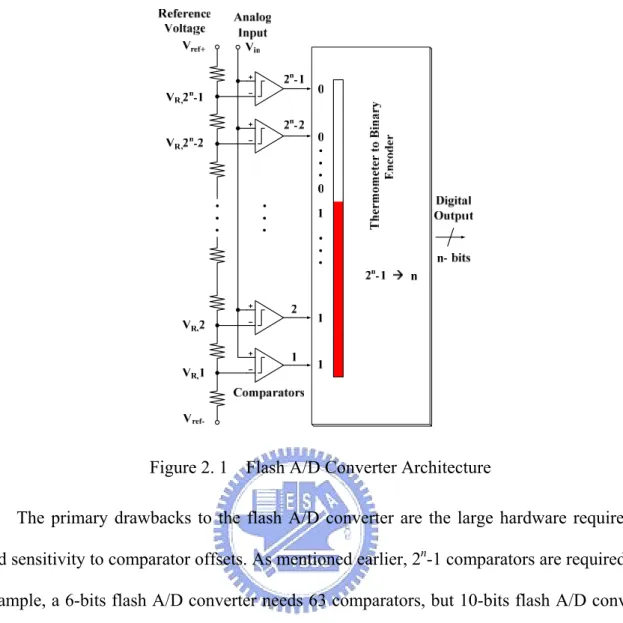
(21) rate of more than 1 GSPS with low resolution. Sigma delta converters are usually the best choice when very high resolution (20 bits or more) is needed. The differences in their architectures make one or the other a better choice, depending on the application. Among the variety of A/D converter architectures, the most popular presently used are flash A/D converter, pipelined A/D converter, and sigma-delta A/D converter [5][6]. In the following sections, these popular A/D converter architectures are briefly described.. 2.1.1 Flash A/D Converter The flash A/D converter architecture, also known as a fully parallel architecture, is fundamentally the fastest architecture. This architecture is conceptually the easiest to understand. An n-bit flash A/D converter consists of an array of 2n-1 comparators and a set of 2n -1 reference values, shown in Figure 2.1. Each of the comparators samples the input signal and compares the signal to one of the reference values. Each comparator then generates an output indicating whether the input signal is larger or smaller than the reference assigned to that comparator. The differences between the input and reference values are amplified to digital levels and generate thermometer code. The encoder converts the thermometer code produced by the comparators to a binary code. As seen from the figure, the comparators all operate in parallel. Thus, the conversion speed is limited only by the speed of the comparator. For this reason, the flash A/D converter is capable of high speed and it is used for high-speed applications such as wireless receiver, digital oscilloscopes, high-density disk drives, and so on.. 6.
(22) Figure 2. 1 Flash A/D Converter Architecture The primary drawbacks to the flash A/D converter are the large hardware requirement and sensitivity to comparator offsets. As mentioned earlier, 2n-1 comparators are required. For example, a 6-bits flash A/D converter needs 63 comparators, but 10-bits flash A/D converter needs 1023 comparators. For this reason, a high resolution flash A/D converter requires a large circuit area and dissipates high power. Furthermore, the large number of comparators present a large capacitance to the output of the sampling circuit. The required comparator offset voltage for a flash A/D converter with n bit resolution is less than 1/2n. At high resolutions, this required comparator offset becomes very small. Because comparators with small offsets are difficult to design and expensive to build and because so many comparators are required, A/D converters with resolutions higher than 8 bits rarely use the flash architecture.. 7.
(23) 2.1.2 Pipelined A/D Converter The pipelined architecture effectively overcomes the limitations of the flash architecture. A pipelined converter divides the conversion task into several consecutive stages. Pipelining enables potentially faster conversion while avoiding the exponential growth of power and hardware. Figure 2.2 illustrates the block diagram of a pipelined A/D converter. The analog input is applied to the first stage in the chain, and N1 bits are detected. The analog residue is also generated and applied to the next stage. The same procedure repeats up to the end of the chain. This concept is similar to the idea of an assembly line because the interstage sampling allows all of the stages to operate concurrently. A common approach to pipelining is based on a precision multiply-by-two stage that merges most of the interstage operations into a compact circuit. Usually used with 0.5 bits of overlap, this technique provides a modular implementation.. Figure 2. 2 Pipelined A/D Converter Architecture The pipelined architecture offers a number of advantages. First, the throughput rate is determined by the speed of only one stage in the pipeline. Second, interstage residue 8.
(24) amplification relaxes the precision required of subsequent stages. Third, the power and hardware of pipelined converters grow almost linearly with the number of bits. Also, overlap and digital correction can be used to allow large offsets in the comparators. The primary drawback of the conventional pipelined topology is the need for high precision in the interstage SHAs, D/A converters, and subtractors, especially at the front end. The precision typically mandates the use of op amps, imposing severe trade-offs among speed, voltage swing, gain, and power dissipation. As device dimensions, supply voltages, and the intrinsic gain (gm ro) of MOSFETs continue to scale down, the design of op amps becomes increasingly more difficult.. 2.1.3 Sigma-Delta A/D Converter The sigma-delta architecture takes a fundamentally different approach than those outlined above. In its most basic form, a sigma delta converter consists of an integrator, a comparator, and a single bit D/A converter, as shown in Figure 2.3. The output of the D/A converter is subtracted from the input signal. The resulting signal is then integrated, and the integrator output voltage is converted to a single-bit digital output (1 or 0) by the comparator. The resulting bit becomes the input to the D/A converter, and the output of the D/A converter’s is subtracted from the A/D converter input signal, etc. This closed-loop process is carried out at a very high “oversampled” rate. The digital data coming from the A/D converter is a stream of “ones” and “zeros,” and the value of the signal is proportional to the density of digital “ones” coming from the comparator. This bit stream data is then digitally filtered and decimated to result in a binary-format output.. 9.
(25) Figure 2. 3 Sigma-Delta A/D Converter Architecture One of the most advantageous features of the sigma-delta architecture is the capability of noise shaping, a phenomenon by which much of the low-frequency noise is effectively pushed up to higher frequencies and out of the band of interest. As a result, the sigma-delta architecture has been very popular for designing low- bandwidth high-resolution A/D converters for precision measurement. Also, since the input is sampled at a high “oversampled” rate, unlike the other architectures, the requirement for external anti-alias filtering is greatly relaxed. A limitation of this architecture is its latency, which is substantially greater than that of the other types. Because of oversampling and latency, sigma-delta converters are not often used in multiplexed signal applications. To avoid interference between multiplexed signals, a delay at least equal to the decimator’s total delay must occur between conversions. These characteristics can be improved in sophisticated sigma-delta A/D converter designs by using multiple integrator stages and/or multi-bit D/A converters.. 2.1.4 Summary of A/D converter Architectures The most popular A/D converter architectures have been reviewed in the previous sections. The flash A/D converter architecture is the fastest, the Sigma-Delta A/D converter is very useful for high-resolution applications, and the pipelined A/D converter can be applied. 10.
(26) for various applications. Each A/D converter architecture has tradeoffs among speed, resolution, and power dissipation. In summary, Table 2.1 provides the characteristics of popular A/D converter architectures [7]. In the third column, “sps” stands for samples per second. The “m” shown in the fourth column is the number of stages in the pipeline architecture.. Architecture Resolution Speed. Latency. (bits). (sps). (cycle). < 10. 250M ~ 2G. 1. Flash. Comments. -high input bandwidth -highest power dissipation -large die size. Pipeline. 8 ~ 16. 1M ~ 200M. m. -high throughput rate -low-power dissipation -on-chip self calibration. Sigma-Delta > 14. > 200K. large. -high resolution -limited sampling rates -digital on-chip filtering. Table 2. 1 Summary of A/D converter architectures. 11.
(27) 2.2 A/D Converter applications There are several applications require the different speed and resolution of A/D converters. Among these are communication, instrumentation, digital audio, digital video, and medical diagnostic equipment [8][9]. With the aid of digital signal processing (DSP), the A/D converter outputs can be processed to bring almost limitless versatility to an application. The basic building blocks of a typical system with a A/D converter include filter for analog input, A/D converter, DSP and memory system, processor and interface system, D/A converter and filter for analog output.. 2.2.1 Fiber-optic Communication High-speed fiber-optic communication requires the analog signal to be converted to digital a A/D converter. Following this the A/D converter outputs must be converted from parallel to serial output format for the driver to modulate a laser diode, as shown in Figure2.4. This allows a single fiber-optic cable to transmit several high-speed signals if necessary. On the other end of the cable, the photodiode detects the digital light pulses, which are then converted to logic level in a parallel format. The D/A converter output is finally filtered by an analog filter. Depending on the application, an option may be to first perform digital filtering before outputting to the D/A converter.. Figure 2. 4 Fiber-optic Communication. 12.
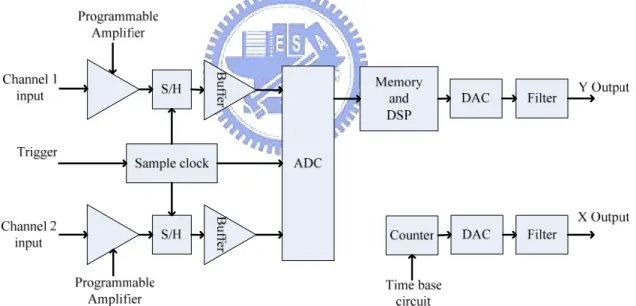
(28) 2.2.2 Digital Oscilloscope A block diagram of a digital storage oscilloscope is shown in Figure2.5. Two input channels are first conditioned by a programmable amplifier. The trigger circuit controls when the sampling starts, which is controlled by sample-and-holds. Buffer amplifiers are required to isolate the low-impedance A/D converter input stage from loading the sample-and-holds. Once digitalized by the A/D converter, the input signals are stored in memory where a DSP can perform several operations (i.e., filtering, averaging, peak-to-peak time versus voltage, root-mean-square, etc.). Two D/A converters then provide both the vertical (signal measurement) and horizontal (time measurement) analog output signals. Finally the analog outputs are filtered before they go to the display driver.. Figure 2. 5 Digital Oscilloscope. 13.
(29) 2.2.3 Medical Imaging The One form of medical imaging is digital x ray (radiography), illustrated in Figure 2.6. With this technique, the images no longer need to be produced or stored on film. Instead, the images are stored within memory for display on a video monitor. In this system the x ray passes through a person onto photomultiplier fluoroscope sensor which converts the x rays to light. The various light intensities are then converted to an analog signal which is filtered before being digitized by the A/D converter. The DSP then enhances the image before driving the output D/A converter for the video image. The advantages to this process are that the time exposure to the x ray for a quality image is significantly shortened and stored images can be manipulated to enhance specific areas.. Figure 2. 6 Digital Radiography System. 2.2.4 CCD Imaging Electronics The charge-coupled-device (CCD) and contact-image-sensor (CIS) are widely used in consumer imaging systems such as scanners and digital cameras. A generic block diagram of an imaging system is shown in Figure 2.7. The imaging sensor (CCD, CMOS, or CIS) is exposed to the image or picture much like film is exposed in a camera. After exposure, the output of the sensor undergoes some analog signal processing and then is digitized by an A/D converter. The bulk of the actual image processing is performed using fast digital signal 14.
(30) processors. At this point, the image can be manipulated in the digital domain to perform such functions as contrast or color enhancement/correction, etc.. Figure 2. 7 Generic Imaging System for Scanners or Digital Cameras. 2.2.5 Touchscreen Digitizers The touchscreens have become widespread in hand held PDAs (Personal Digital Assistants) and other computer products. The majority of PDA makers use a four-wire resistive element as the touchscreen due to its low cost and simplicity. For the touchscreen to interface with the host processor, analog waveforms from the screen must first be converted to digital data . The user enters data on the screen with a stylus. An A/D converter converts this analog information to digital data that the host microprocessor uses to determine the stylus's position on the screen. During coordinate measurement, one of the resistive planes is powered through on-chip switches on the controller A/D converter. For X coordinate measurement, the X plane is powered. The Y plane senses where the pen is located on the powered plane. When the pen depresses on the screen, the planes short at this location (shown as the dotted line in the diagram). The voltage detected on the sense plane is proportional to the location of the touch on the powered plane. The four -wire resistive touchscreen interface for X coordinate measurement as shown in Figure 2.8. The Y coordinate can be measured by applying power to the Y plane, using the X plane to sense the position. Thus, X and Y coordinates can be 15.
(31) digitized from the screen. The digital code is then operated on by the host CPU, and character recognition and position information can be achieved.. Figure 2. 8 Four-Wire Resistive Touchscreen Interface. 2.2.6 Digital Audio Modern wireless systems, such as cellular telephone, use low pass filter, high resolution A/D converters, digital signal processor (DSP) and high resolution D/A converters. The modern cell phone handset block is shown in Figure 2.9.When we speak to other person with cell phone, the low pass filter remove noise from voice, A/D converter transform voice into digital signal and then the digital signal is dealt with DSP. Modern cellular transmission systems make use of DSP-based speech compression algorithms in order to reduce the overall data rate to acceptable levels, rather than limiting the resolution of the converters. Digital audio systems place high resolution demands on A/D converters and D/A converters because of the wide dynamic range requirements. The digital audio signal may then be stored or transmitted. Digital audio storage can be on a flash memory, or any other digital data storage device. Audio data compression techniques — such as MP3— are commonly employed to reduce the size. Digital audio can be streamed to other devices. The last step for digital audio 16.
(32) is to be converted back to an analog signal with a D/A converter.. Figure 2. 9 Modern Cell Phone Handset block. 17.
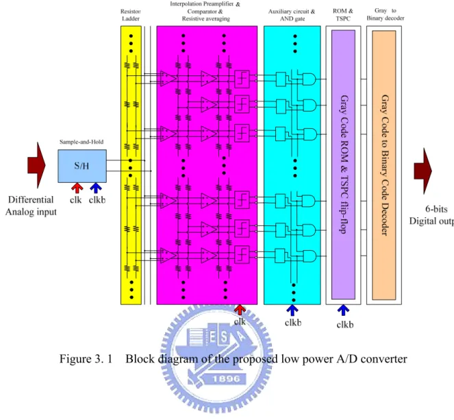
(33) CHAPTER 3 Low-Power High-Speed Techniques and Circuit Design In this chapter, the low-power high-speed architecture is proposed to reduce the input capacitance, offset errors, power dissipation, bubble errors and metastability errors by using sample-and-hold, interpolation, averaging and digital error correction techniques. With the architecture, the dynamic performance is improved, the input capacitance is reduced, 83% power saving in preamplifiers is achieved and the power of (2n-1)m pipeline latches is removed. The circuit design and related issues will be discussed in detail. The required resolution is 6 bits and the sampling rate is 2GHz. As the result, circuit design plays an important role to achieve the specifications. The block diagram of the proposed A/D converter is shown in Figure 3.1. The proposed A/D converter consists of analog part and digital part. The analog part consists of sample-and-hold, resistor ladder, interpolation preamplifiers, comparators and resistive averaging. The digital part consists of auxiliary circuit, AND gates, ROM, TSPC, Gray-to-binary decoder, clock generator and output buffer. The design issues of each component are discussed step by step. Finally, the static and dynamic performances simulation results are presented in the last section.. 18.
(34) Figure 3. 1 Block diagram of the proposed low power A/D converter. 3.1 Sample-and-Hold Technique The purpose of the sample-and-hold (S/H) circuit is to track and hold the input signal long enough for the A/D converter to complete a conversion without appreciable error. The S/H circuit is a crucial part, especially for high speed sampling rates. To improve the dynamic performance of the A/D converter, a S/H circuit can be put in front of the converter. By holding the analog sample static during digitization, the S/H largely removes errors due to skews in clock delivery to a large number of comparators, limited input bandwidth prior to latch regeneration, signal-dependent dynamic nonlinearity, and aperture jitter. The distributed time skew problem of quantization is alleviated as a result of the usage of the front-end S/H 19.
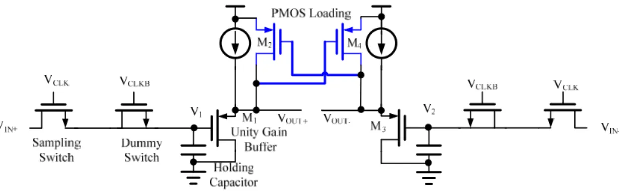
(35) circuit. For gigahertz sampling rate operation, S/H becomes essential to achieve the desired converter resolution with wide input bandwidth. Closed loop configuration provides good linearity and dynamic range but cannot achieve very high speeds. In order to operate at high speed, the S/H has to be a simple open-loop configuration. The basic S/H configuration shown in Figure 3.2 consists mainly of a sampling switch and a holding capacitor [3]. This single ended configuration makes it possible to design for very high speed, but it has signal-dependent charge injection and clock feedthrough.. Figure 3. 2 Basic S/H Configuration The pseudo-differential type S/H configuration shown in Figure 3.3 is the best choice to solve signal-dependent charge injection and clock feedthrough. This type S/H consists of sampling switches, dummy switches, holding capacitors, and unity gain buffers. The dummy switches are driven by reverse of the clock signal and they are used to reduce the effect of signal-dependent charge injection and clock feedthrough released from the sampling switches [2]. The holding capacitors are made large enough to overcome the gate capacitance variation of the MOSFET. The buffer is made by PMOS whose bulk is connected to its source to suppress the body effect.. 20.
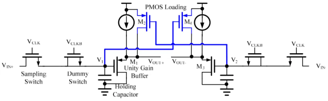
(36) Figure 3. 3 Pseudo-Differential Type S/H Configuration In Figure 3.3, the constant current source follower is the simplest realization of a unity gain buffer. But, it still has limitation and drawback. When the input to the buffer is fast and has large amplitude, the skew rate at the output of the circuit is limited. Thus, its speed can not be linearly improved by increasing the bias current. Although we can suppress the body effect by connecting its bulk to source, its gain still can not reach real unity. Due to the finite output resistance, its gain can only approximate 0.9. The buffer with this gain will degrades the amplitude of output signal when input frequency is very high. So, adding a PMOS loading to increase output resistance can make the gain approximates unity.. Figure 3. 4 The first cross-coupling type S/H Configuration with a PMOS Loading. 21.
(37) Figure 3. 5 The second cross-coupling type S/H Configuration with a PMOS Loading. There are two cross-coupling types of the S/H configuration and their gain can achieve unity. The first cross-coupling type is shown in Figure 3.4 and second cross-coupling type is shown in Figure 3.5. The gain of the first cross-coupling type S/H configuration is given by (detailed analysis is shown in Appendix):. VOUT + ro1ro 2 = ( g m1 + g m 2 ) ≤ 1 V1 ro1 + (1 + g m1ro1 ) ro 2. (3.1). and its 3db frequency is given by (detailed analysis is shown in Appendix):. f 3 db = f1 =. 1 2πτ 1. =. 1 2πC gs1 ( ro1 // ro 2 ). (3.2). The gain of the second cross-coupling type S/H configuration is given by (detailed analysis is shown in Appendix): ' VOUT ro'1ro' 2 g m' 2 g m' 1ro'1 ' + = ' ( g m1 + ) ≥1 V1' ro1 + (1 + g m' 1ro'1 ) ro' 2 1 + g m' 1ro'1. (3.3). and its 3db frequency is given by (detailed analysis is shown in Appendix):. f 3'db = f1' =. 1 2πτ 1'. =. 1 2πC gs' 1 ( ro'1 // ro' 2 ). (3.4). Give a sinusoidal input waveform with amplitude A and radian frequency ω and assume. 22.
(38) unity gain buffer is one pole transfer function as follows:. A. A(ω ) =. 1+ (. ω 2 ) ω 3 db. (3.5). If the tolerable output amplitude error is lower than 2% (6 bits accuracy), we have. 1−. 1. ω 2 1+ ( ) ω 3 db. < 0.02 , and then. f 3 db ≥. 1G = 4.926 G 0.203. (3.6). Figure 3. 6 The simulation of the first and second type S/H The simulation of the first and second cross-coupling type S/H configuration is shown in Figure 3.6. From this figure, the gain of the first cross-coupling type S/H configuration approximates unity and its 3db frequency is 5.33GHz. The gain of the second cross-coupling type S/H configuration is larger than unity and its 3db frequency is 2.39GHz. From equation (3.6), the buffer 3db frequency must be high than 4.926GHz. Thus, the first cross-coupling type S/H configuration fits the design requirement and the 3db frequency is 5.33GHz. The proposed design can achieve the wide bandwidth to get high dynamic performance. 23.
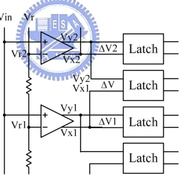
(39) 3.2 Interpolation Technique It is needless to say that the number of elements and the power dissipation increase exponentially to the resolution of flash A/D converter. The flash A/D converter architecture is considered to realize the highest conversion frequency, however, it suffers from not only large chip size and large power dissipation, but also lower dynamic performance due to large input capacitance [10]. Hence, some circuit techniques that can reduce the element count are required. Interpolation technique is the good solution to solve these problems. The interpolation architecture of preamplifier is shown in Figure 3.7. △V1(=Vy1-Vx1), △ V2(=Vy2-Vx2), △V(=Vy2-Vx1) are the outputs of the preamplifiers, Vin is the input voltage and Vr1, Vr2, Vr are the reference voltages.. Figure 3. 7 Interpolation Preamplifier Architecture Interpolation allows the generation of intermediate voltages, so that the input voltage does not need to be compared to 63 distinct reference voltages at the front-end of a flash A/D converter. Each input to reference voltage comparison at the front-end would require its own preamplifier, consuming an unacceptable amount of power and area. Virtual zero crossing. 24.
(40) points shown in Figure 3.8, which are not the result of the input crossing a physical reference voltage, are created through interpolation at amplification stage. In other words, in this scheme a zero crossing is obtained by interpolating between two reference levels. Performance indices of the preamplifier such as input common-mode range, input capacitance, power dissipation, overdrive recovery speed, voltage gain, and capacitive feedthrough to the reference resistor ladder often place tight requirements on the preamplifier. Thus, using interpolation to reduce the number of preamplifiers relaxes its design requirements and can improve the differential nonlinearity [11]. However, there are some design conditions which need to be considered. Interpolation is only between close-enough preamplifier outputs to avoid non-linear zero crossing. The size of the input transistors of the preamplifier needs to be increased. Larger size can reduce the offset from the preamplifier itself. The gain of the preamplifier needs to be tuned well. Small gain of the preamplifier can not overcome the offset from comparator, but large gain of the preamplifier can cause no gain error at zero crossing shown in Figure 3.9. If no gain error at zero crossing happens, the preamplifier can not reduce the offset from the comparator. The only adequate gain of the preamplifier can generate the good zero crossing shown in Figure 3.8.. Figure 3. 8 Good Zero Crossing. 25.
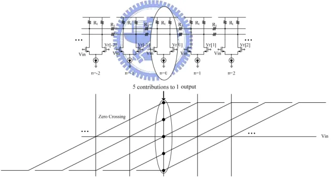
(41) Figure 3. 9 No Gain Error at Zero Crossing. 3.3 Averaging Technique High speed flash A/D Converter with medium resolution usually employs differential pairs as pre-amplifying stages before the comparators. Their offset voltages are the ultimate limitation to the linearity that may be achieved by the A/D converter. Increasing the area of the components in the differential pairs reduces offset voltages , but increases parasitic capacitances, leading to a large power dissipation, large die size and large input capacitance or to the reduction of the maximum operating frequency [12]. To partially overcome this problem an averaging scheme will be introduced. This averaging scheme uses the outputs of more active input pairs to increase the effective gate area and in this way reduce the offset voltages. The figure 3.10 shows five differential preamplifiers with load resistor R0 as part of the input preamplifier chain used in flash A/D converter. Averaging is obtained by coupling the outputs of the differential preamplifiers via averaging resistor R1. This averaging resistor chain continues to couple more input stages. As long as the input preamplifiers are active and operate in the linear signal range, then the 26.
(42) output signal of these active preamplifiers contribute via the averaging resistors to the signal of a differential preamplifier operating around the zero crossing level. Here preamplifier (n=0) is supposed to be the zero crossing preamplifier. The output signals from the left neighbors of the zero crossing preamplifier influence the zero crossing. The same effect is obtained from the right neighbors. As long as the neighboring preamplifiers are in the linear region it looks like that the zero crossing amplifier consists of a much bigger device with a size equal to the sum of the areas of the active linear amplifiers [3]. By adding resistors R1, not only the offset error (noise) is reduced but also the gain of the preamplifier (signal) is loss. In order to reduce the effective gain of error but one of the signal is maintained, the resistive ratio of R1/R0 have to be choice properly to perform optimum.. Figure 3. 10. Resistive Averaging Scheme and Zero Crossing. 3.3.1 Spatial Filtering of the Averaging Resistive Network 27.
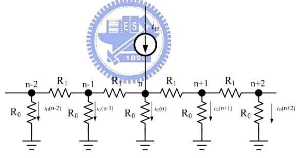
(43) The averaging requires the summation of quantities spread into two or more samples in either time or space. In the MOSFET example, the parallel connection spreads the noisy charges. Similarly in the preamp array of a flash A/D converter the output current spreads through the lateral connections in the averaging resistor network. Summation is automatic when physical quantities such as currents and charges merge at a node in accordance with Kirchhoff’s laws. The impulse response of the spreading network, which forms a spatial filter, characterizes the extent of spreading. Usually the wider the impulse response will get the higher the SNR. However, there are limits to this in uses such as offset averaging, where a wider impulse response also filters out signal. To correctly optimize the SNR, the properties of both signal and noise must be taken into account to find the best impulse response. Figure 3. 11. The impulse Response of a resistor network as spatial filter. The impulse response, h(n), of the spatial filter is found by injecting a unit stimulus current at one node, and noting the resulting distribution of current in each R0 at other nodes as shown in Figure 3.11. For a stimulus current iin injected to an arbitrary node n, Kirchhoff’s current law (KCL) requires that. iin − io ( n ) + (io ( n − 1) − io ( n )) R0 / R1 + (io ( n + 1) − io ( n )) R0 / R1 = 0 28. (3.7).
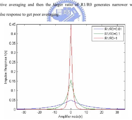
(44) where the third and fourth terms are the currents flowing into node n from node (n-1) and (n+1), respectively. Using the transform simplifies analysis. Applying the z transform to (3.7). H ( z ) = I o ( z ) / I in ( z ) = (1 + 2( R0 / R1 ) − ( R0 / R1 )( z + z −1 )) −1. (3.8). The inverse transform H(z) of yields the spatial impulse response [13]. h ( n ) = h ( 0 )b. n. , where. b=e. − a cosh( 1+ R1 / 2 R0 ). <1. (3.9). h (0) is a normalized coefficient. Uniform current division in the R0- R1 network leads to an impulse response that decays exponentially in n. The width of the impulse response can be controlled by the ratio of R1/R0 as shown in Figure 3.12. The impulse response acts as a low pass filter in spatial domain and the width of impulse response will influence the averaging effect. The smaller ratio of R1/R0 generates wider width of the impulse response to get effective averaging and then the larger ratio of R1/R0 generates narrower width of the impulse response to get poor averaging.. Figure 3. 12. Impulse response as a function of resistive ratio R1/R0 at node(0). 29.
(45) 3.3.2 Error Correction Factor (ECF) The parameter used to the averaging performance is error correction factor (ECF) [13]. The error correction factor is defined as ratio standard deviation of the original offsets and standard deviation of the input-referred offsets after averaging. Thus. σ os g m′ (0) / g m (0) = σ os′ σ (ios′ ) / σ (ios ). ECF ≡. (3.10). Where σ os ( σ os′ ), σ (ios ) ( σ (ios′ ) ) and g m (0) ( g m′ (0) ) represent standard deviation the input referred offset voltage, offset current and transconductance of the preamplifier before (after) averaging at the zero crossing node. Now let us derive the ECF for a spatial filter with the impulse response given by equation (3.9). Since the output of any filter is found by convolving its input with the impulse response, we have ∞. (WZX −1) / 2. −∞. − (WZX −1) / 2. g m′ (0) = ∑ g m ( n ) h (0 − n ) = g m. ∑. h(n) (3.11). Where WZX is the width of linear active region of the preamplifier which can be expressed as. WZX = 2 2Veff / LSB. .The output noise current is given by. ios′ (0) =. (Wn −1) / 2. ∑. − (Wn −1) / 2. ios ( n) h(0 − n ) (3.12). which leads to the standard deviation. σ (ios′ ) ≡ i ′ = σ (ios ) 2 os. (Wn −1) / 2. ∑. − (Wn −1) / 2. h 2 (n) (3.13). Where Wn is the width of noise window of the preamplifier. Combining Equation (3.10), (3.11), (3.12) and (3.13), the ECF can be shown that. 30.
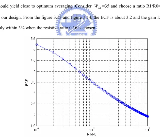
(46) ECF =. (1 + b ⋅ (1 − 2b (WZX −1) / 2 )) /(1 − b) (1 + b 2 (1 − 2b (Wn −1) )) /(1 − b 2 ). where. b=e. − a cosh( 1+ R1 / 2 R0 ). (3.14). Figure 3.13 shows the error correction factor (ECF) respects to resistive ratio R1/R0. How accurate must be the ratio of R1/R0 to deliver near optimum benefits? The ratio is chosen larger than at the maximum point to prevent the gain loss. The resistive network causes the gain loss of the preamplifier as shown in Figure 3.14. The value of ECF will be higher if the value of R1/R0 is lower, but it also causes the gain loss of the preamplifier when the value of R1/R0 is lower. For example, if the ratio falls by 50% to 0.08, the ECF increases from 3.2 to 3.7 but gain loss increases from 3% to 11%. If rises by 50% to 0.24, the ECF also falls to 2.8 but gain loss approaches zero. Thus, a network with only roughly the right resistor ratio should yield close to optimum averaging. Consider WZX =35 and choose a ratio R1/R0=0.16 in our design. From the figure 3.13 and figure 3.14, the ECF is about 3.2 and the gain loss is only within 3% when the resistive ratio 0.16 is chosen.. Figure 3. 13. The error correction factor verse resistive averaging ratio. 31.
(47) Figure 3. 14. Figure 3. 15. Gain loss verse resistive averaging ratio. Monte-Carlo simulation setup scheme. 32.
(48) Figure 3. 16. The preamplifier Monte-Carlo analysis with and without averaging resistor. Monte-Carlo analysis is performed to verify the benefits of resistive averaging. Figure 3.15 shows the Monte-Carlo simulation setup scheme. The parameters for the device mismatch including threshold voltage mismatch and resistor mismatch are provided by foundry []. In the idea case with no transistor mismatch, the comparator output changes polarity when a slow ramp input cross the corresponding threshold. Figure 3.16 shows that the time the comparator changes polarity is randomly dispersed with respect to when the input cross zero. The preamplifier offset set voltage is 12mV when the preamplifier without averaging resistor. Using averaging resistor, the preamplifier offset reduce to 4.1mV. The simulation result is shown in Figure3.16; it is a composite plot of 60 Monte-Carlo transient analyses.. 3.3.3 Nonlinearity Error and Compensation at the Edges Finiteness of the array of preamplifiers poses unique problems at the edges of an. 33.
(49) averaging flash A/D converter. Usually the preamplifier array comes to an end at the upper and lower limits of the analog full scale. This will disrupt averaging at the last few preamplifiers, because at the extreme nodes there is no longer an equal number of stimuli into the resistor network from both left and right. As shown in Figure 3.17 the vertical line that crosses the zero-crossing point at the right-hand extreme of full scale intercepts zero-crossings only in the upper half plane if there are no dummy zero-crossings. In presence of the lateral resistors, those intercept points contribute positive currents to the zero-crossing node and effectively pull the zero-crossing toward the center of the array. Unless the positive intercept points are balanced with negative ones from dummies or by distorting reference taps, all the zero-crossings within the range of half width of impulse response at each edge are pulled resulting a systematic INL curvature.. Figure 3. 17. Dummy preamplifiers to reduce edge effects. Linearity across the full scale requires that no distortion should build up at the edges. A straightforward solution is to add preamplifiers on either edge of the array to extend the averaging network by at least width of the impulse response, the extent of the interaction range [13]. Therefore, half number of dummy preamplifiers is attached at each end. The current flowing in averaging resistor shows a large bending at both ends, as shown in Figure 3.18. 34.
(50) Figure 3. 18. The current flowing in resistive network shows the boundary condition. Figure 3. 19. Dummy preamplifiers with cross connection averaging. 35.
(51) Figure 3. 20. Impulse response as a function of resistive ratio R1/R0=0.16 at node(0). This bending is of a form as the low-to-high current in the lowest edge and the high-to-low current decreasing in the highest edge, causing the INL pattern at edge to go opposite direction. In order to keep the symmetry condition at the edge of preamplifiers, the dummy preamplifiers are added and the cross connection averaging resistor is adopted which is shown is Figure 3.19. The numbers of dummy preamplifiers are probably equal to the range of impulse response which is shown in Figure 3.20. In this design the range of impulse response of the averaging networking is about 16 dummy preamplifiers are enough to compensate the integral nonlinearity errors at the boundary condition. Figure 3.21 shows the simulation at the boundary condition with and without the dummy preamplifiers.. 36.
(52) Figure 3. 21 Averaging current following in the load resistance From this figure, the nonlinearity error is serous obviously at the edge of preamplifiers and the linearity range is extended with proper dummy preamplifiers at the boundary of preamplifiers array.. 3.3.4 Power Saving in Preamplifiers Array Averaging resistors are used in both preamplifiers and comparators in order to reduce the input referred offset. For unaveraged preamplifier, the standard deviation of input referred offset σ(ΔVos) is inverse proportional to the square root of the size (WL) of the input differential pair [14] as derived in Equation 3.11. With averaging resistors, the offset can be reduced by κ times. Therefore, for the same offset specification, the size of each preamplifier can be reduced κ2 times compared with unaveraged one.. 37.
(53) 1 WL. σ (ΔVos ) ≈ σ (ΔVth ) ∝. (3.15). With the same preamplifier speed, overdrive condition and input-referred RMS offsets, the current consumption of the preamplifier is proportional to the size of the input differential pair is derived in Equation 3.12. Hence, the size reduction in preamplifiers also leads to power reduction and the power reduction factor is κ2. In our averaging resistor design, the optimum κ is about 3 that is 9 times power reduction in a single preamplifier [15].. Speed ≈. 2 I / Veff gm I ≈ ∝ 2πC gs 2π (2 / 3)WLCox WL. (3.16). Usually some dummy preamplifiers are required at the boundary to eliminate the linearity error due to the edge effect. Including the dummies, the total power dissipation in preamplifiers is scaled down as. Ptotal ,avg Ptotal ,unavg. = =. N avg N unavg N avg N unavg. × ×. Pavg Punavg. =. N avg N unavg. (WL) avg (WL) unavg. ×. I avg I unavg. N dummy ⎞ 1 ⎛ ⎟⎟ × 2 = ⎜⎜1 + n 2 1 − ⎝ ⎠ k. (3.17). where Ptotal,avg (Ptotal,unavg) represents the total power dissipation of the preamplifier array with (without) averaging resistors; Navg (Nunavg) represents the number of the preamplifiers with (without) averaging resistors; Pavg (Punavg) represents the power dissipation of a single preamplifier with (without) averaging resistors. Ndummy is the number of dummy preamplifiers and n is the resolution of the A/D converter. In our case, the total power of preamplifier array scaled down factor is 0.168 that is about 83% power reduction, exhibiting low power performance.. 38.
(54) 3.4 Digital Error Correction Technique Comparators in a flash converter generate what is commonly known as a thermometer code. If a particular comparator’s reference point is below the level of the input signal, the comparator’s output is high; if the reference point is above the input, its output is low. It is easy to see why this code is called thermometer code. With an increasing input signal the number of ones is increasing. When everything is working ideally, the collection of comparator outputs should resemble a thermometer: all zeros above the input level and all ones below the input level. The zero-to-one transition point rises and falls within the input level. The thermometer code is translated to a final binary output word using the zero-to-one transition point to address a ROM. A high speed flash A/D converter with this type of the digital encoding structure typically suffers from two problems: bubble errors (or sparkles) in the thermometer code and metastability errors. The purpose of the digital encoding is to convert the comparator outputs into a 6-bits code word and to suppress the errors caused by the comparator metastability and bubble errors in the thermometer code. Thus, the digital encoding with the digital error correction is very important to achieve good resolution at high input frequencies.. 3.4.1 Bubble Error Correction Under extremely high input slew rate conditions, timing differences between the clock lines and signal lines can cause the effective sampling moments between comparators to be different. This can cause a bubble in the thermometer code where a one may be found among zeros. This is normally called a bubble in the thermometer code, because this error resembles bubbles in the mercury of a thermometer.. 39.
(55) Figure 3. 22. Three input AND gate to solve a bubble error. Bubble errors result from three major sources [2]. First, the large overall input-referred random offset can switch the order of the two adjacent thresholds and create bubble errors. Second, the slew-dependent sampling and clock dispersion between comparators cause bubble errors. Finally, the propagation-delay variations through the preamplifier stage as a result of limited bandwidth and fast input frequency worsen the bit-error rate to generate bubble errors. To overcome this problem a bubble correction method can be used. A common method of suppressing bubbles is to use what amounts to a three-input AND gate to address the ROM. For example, two zeros have to be found above a one to cause the ROM line to go high. Then a sample correction of a bubble error in the thermometer code can be corrected as shown in Figure 3.22.. 3.4.2 Metastability Error Correction When the applied input signal is near the reference voltage for a comparator, the comparator output may be undefined at the end of evaluation time and then metatstability in a 40.
數據
+7
相關文件
In this chapter, a dynamic voltage communication scheduling technique (DVC) is proposed to provide efficient schedules and better power consumption for GEN_BLOCK
In this chapter, we have presented two task rescheduling techniques, which are based on QoS guided Min-Min algorithm, aim to reduce the makespan of grid applications in batch
To reduce the leakage current related higher power consumption in highly integrated circuit and overcome the physical thickness limitation of silicon dioxide, the conventional SiO
To reduce the leakage current related higher power consumption in highly integrated circuit and overcome the physical thickness limitation of silicon dioxide, the conventional SiO 2
Filter coefficients of the biorthogonal 9/7-5/3 wavelet low-pass filter are quantized before implementation in the high-speed computation hardware In the proposed architectures,
GaN transistors with high-power, High temperature, high breakdown voltage and high current density on different substrate can further develop high efficiency,
In this paper, we discuss how to construct low-density parity-check (LDPC) codes, and propose an algorithm to improve error floor in the high SNR region by reducing the
A segmented current steering architecture is used with optimized performance for speed, resolution, power consumption and area with TSMC 0.18μm process.. The DAC can be operated up
