國 立 交 通 大 學
電子工程學系 電子研究所碩士班
碩 士 論 文
新穎的功率電晶體於熱載子效應之特性化分析
及模型建立
Characterization and Modeling of Novel Pseudo-Drain(PD) RF Power
CMOS under Hot Carrier Stress
研 究 生 : 陳 勝 杰
指導教授 : 張 俊 彥 博士
新穎的功率電晶體於熱載子效應之特性化分析
及模型建立
Characterization and Modeling of Novel Pseudo-Drain(PD) RF Power
CMOS under Hot Carrier Stress
研 究 生:陳 勝 杰
Student:Sheng-Jay Chen
指導教授:張 俊 彥 博士
Advisor:Dr. Chun-Yen Chang
國 立 交 通 大 學
電子工程學系 電子研究所碩士班
碩 士 論 文
A Thesis
Submitted to Institute of Electronics
College of Electrical Engineering and Computer Science
National Chiao Tung University
in partial Fulfillment of the Requirements
for the Degree of
Master of Science
in
Electronic Engineering
September 2008
Hsinchu, Taiwan, Republic of China
新穎的功率電晶體於熱載子效應之特性化分析
及模型建立
學生: 陳 勝 杰
指導教授: 張 俊 彥 博士
國立交通大學
電子工程學系 電子研究所碩士班
摘要
在最近幾年,先進的CMOS技術已經成熟的應用在射頻RF (radio-frequence)這塊領域上 面,像是無線通訊系統、藍芽技術的應用、WLANs以及超寬頻(ultra-wide band)等等。而微 波元件又是通訊系統中最重要的骨架。當中又以矽為基底的金氧半場效電晶體已經成為射 頻元件的主流。 整合的功率放大器對於SOC的應用上相當重要,因此發展適用的功率電晶體是必須 的。而功率電晶體則需要可以承受較高的崩潰電壓以達到傳送較高能量和附加功率效能的 功用。但傳統CMOS技術的缺點就是限制住輸出的崩潰電壓,這對於RF方面的應用而言, 是一種矛盾的關係。所以一些文獻提出了改進的方法,諸如Drain-extended MOS (DEMOS)以 及Lateral-Diffused MOS (LDMOS) transistors都可以提高崩潰電壓,但是他們在高頻特性的表 現上面,卻沒有這麼地理想。於是我們利用UMC的製程技術,從DEMOS的結構上去改變以達到改善的效果。而這新 的元件命名為Pseudo-drain MOS (PDMOS)。本篇論文的重點即是討論這顆改善後新元件的直
流特性和高頻特性,並將其結構做些改變,再將改變前後的兩個不同結構深入比較受到熱 載子效應後的直流特性和高頻特性以及功率特性方面的行為,更進一步分析在熱載子效應 下的可靠度比較。 最後,透過小訊號模型的建立,經由討論各別小訊號參數的變化情形,我們發現金氧 半場效電晶體的互導,汲極到源極的電阻以及閘極到源極的電容還有汲極的電阻受到熱載 子效應影響較大,特別是汲極電阻的變化,也輔助說明了這兩種不同結構在直流特性上的 差異性。
Characterization and Modeling of Novel Pseudo-Drain (PD)
RF Power CMOS under Hot Carrier Stress
Student: Sheng-Jay Chen Advisor: Dr. Chun-Yen Chang
Institute of Electronics
National Chiao Tung University
Abstract
In recent years, advanced CMOS technologies have been investigated and pushed to perform well in RF areas, like in wireless systems: Bluetooth applications, WLANs and UWB (ultra-wide band). Microwave transistors are the backbone of these modern wireless communication systems. Since the Si-based MOSFETs (metal-oxide-semiconductor field-effect transistors) have become the mainstream of RF transistors in recent years.
The integration of the power amplifier for SOC realization is very important. Hence, the development of suitable power cells using MOS transistors is necessary to achieve this goal. Power transistors with high breakdown voltage are required to achieve higher power delivery and power added efficiency (PAE).But, the drawback of CMOS technology is the inherent limitation of a lower output breakdown voltage, and it is incompatible for RF power applications. Therefore, some literatures which addressed this issue introduced devices like the “Drain-extended” MOS (DEMOS) and the “Lateral-Diffused” MOS (LDMOS) transistors to obtain a higher breakdown voltage and power performance. However, the high frequency characteristics were degraded.
In this thesis, we improved the performance from DEMOS by UMC technologies. And the new device is named Pseudo-drain MOS (PDMOS). The purpose of this thesis is to investigate the DC characteristic and RF characteristic of this new RF MOSFETs and then we do some variation on structures. Besides, we compare to go deep into the DC characteristic, RF
characteristic and power performance which suffer hot carrier stress on different structure from changing before and after. Then we try to analyze the reliability under hot carrier stress.
Finally, by way of building a small-signal model, we proposed that individually parameter after hot carrier HC stress, the transconductance(gm0), drain-to-source resistance(Rds),
gate-to-source capacitance(Cgs), and drain resistance(Rd) suffer more degradation after HC stress.
Especially the variation on drain resistance(Rd) could explain the difference between these two
誌 謝
時序入秋,伴隨而來的是學生時代的告一段落,而此論文,也即將一併完成。兩年多 來,許多血汗交織而成的歡笑、滿佈朦朧霧氣的美麗清晨、那環境清幽的宜人校園、還有 嚴謹卻又不失歡笑的電資大樓 418 實驗室、以及成群可愛的校狗們,都將封裝成冊,收入 心底成為回憶。 在此,首要特別感謝的是我的指導教授張俊彥院士,讓我親身感受到老師對實驗的熱 忱與執著,在學術上嚴謹且宏觀的看法,也進一步的開拓了我不同的思維與氣度。感謝陳 坤明博士在實驗上提供了完善的設備及資源,以及研究所兩年來不厭其煩的教導,憑藉其 過人的學術修養,讓我在這裡求得更完善的知識。再來是胡心卉學姊,總在我困頓迷惑之 時,適時的給予我明燈,耐心的指引並且幫助我,給我最恰當的建議,使得實驗等各方面, 都得以順利完成,非常感謝老師、學長、姊的教導。 而在儀器的使用方面,感謝國家奈米元件高頻實驗室黃國威博士大力支持,以及各工 程師的鼎力協助,特別是汶德,柏源學長,幫我解決了不少量測上的問題。還有感謝聯華 電子公司的黃聖懿學長在提供晶圓上面的幫忙與協助。 這些日子以來,總少不了朝夕相處的學長姐,同學,學弟們,感謝你們的陪伴,沒有 你們,也不會有這本論文的誕生。感謝宗火喜、峻豪、心卉、兆欽、立偉、怡誠、緯仁、 弘斌、哲榮、詩國、小丞丞、彥廷等學長姐們,謝謝你們在實驗上的幫忙,研究上的態度, 以及做人處事的基本修養,還有你們撐起的實驗室,都讓我獲益良多。 同時也要感謝我的同學們,成能、貴宇、培堃、述頴、欣哲、効諭、宣凱、筱函、敬 倫、弘森、嘉文、毅函等,有你們的陪伴,在這裡一起做實驗,一起瘋,一起歡笑,一起 度過每個寒暑時節,每個辛勤的白晝,每個歡笑的夜晚,都是我一生最難忘的回憶。還有 誌陽,耀峰、信淵等學弟們,在生活上及實驗方面的幫忙與協助,以及替這間實驗室,創 造了不少和諧歡愉的氣氛,由衷的感謝你們。 還要特別感謝我的大學同學根生、韋志、原江、建倫等、高中同學耀輝、傳恕、鈞毅、 景鴻等,在我背後給我最大的動力,讓我走的更順,更平穩。 最後,也是最重要的,感謝我親愛的爸爸陳福林先生、媽媽張金玲女士、妹妹亦禎, 謝謝你們始終默默支持著在外地求學的我,於精神和生活上給予我最大的鼓勵與協助,也感謝你們體諒我這段日子和家人相聚時間變少,更提供一個溫暖的家,讓我無後顧之憂的 完成這個碩士學位,這些日子以來,辛苦你們了。也感謝佳珣兩年多來對我的包容與體諒, 一起走過屬於我們的時光。於此,僅以這本論文獻給你們。
Contents
Abstract (Chinese)
i
Abstract (English)
iii
Acknowledgement
v
Contents
vii
Table Captions
ix
Figure Captions
x
Chapter 1
Introduction
1.1 RF Transistors
1
1.2 Basic Concept of RF MOSFETs
2
1.3 Hot Carrier Reliability of RF MOSFET
3
Chapter 2
Basic Theory and Experiments
2.1 Hot Carriers Mechanism
5
2.2
Oxide
Breakdown
Mechanism
7
2.3 Device under Test and Measurement
Techniques
8
2.3.1
Device
under
Test
8
2.3.2 I-V Measurement
8
2.3.3
High
Frequency
Characteristics
Measurement
9
2.3.4
Output
Power
Measurement
9
Chapter 3
3.1
Device
Fabrication
and
Design 14
3.2
Compare
with
DC
Performance
15
3.3
Compare
with
RF
Performance
15
3.3.1
Experimental
Procedures 15
3.3.2 RF Performance
16
3.3.3
RF
Power
Performance
16
3.3.4 RF Linearity
17
3.4 Summary
18
Chapter 4
Characteristics of RF MOSFETs under Hot Carriers Stress
4.1
HC
Stress
Experiments
26
4.2
Effect
of
HC
Stress
on
DC
Characteristics
27
4.3 Effects of HC Stress on Cut-off Frequency and Maximum
27
4.4 HC Effects on Power Performance
and
Linearity
29
4.5 Summary
30
Chapter 5
Modeling of RF MOSFETs under HC stress
5.1 Extraction Method of Small-Signal Model Parameters
48
5.2
Modeling
of
PDMOS
under
HC
Stress
50
5.3 Summary
51
Chapter 6
Conclusions
6.1 Conclusions
69
TABLE CAPTIONS
CHAPTER 1
Table 1-1 Performance of CMOS technology in several generations
4
CHAPTER 3
Table.3-1 Extracted model parameters of HV01 and HV02
19
Table.3-2 Extracted
power
parameters
of
HV01,
HV02
19
CHAPTER 4
Table.4-1
Extracted linearity parameters of HV01, HV02
31
CHAPTER 5
Table 5-1 (a) Extracted parameters before and after HC stress condition B
on
HV01;
(b)
Extracted
parameters before and after HC stress
condition
B
on
HV02;
(c) Extracted parameters before and after
HC
stress
condition
C on HV01; (d) Extracted parameters before
and
after
HC
stress
condition
C
on
HV02
53
FIGURE CAPTIONS
CHAPTER 1
Fig. 1-1 Schematic of a typical bulk MOSFET structure
4
CHAPTER 2
Fig. 2-1 (a)Channel hot electrons (b) Drain avalanche hot carriers
(c) Substrate hot electrons
11
Fig. 2-2 (a) Schematic illustrating the trapping of tunneling electrons
(b) Schematic illustrating the generation of an electron-hole pair in the
anode by a tunneling electron (c) Schematic illustrating the trapping of
holes
in
the
oxide
layer
12
Fig. 2-3 (a) Block diagram of the load-pull measurement system.
(b) Power contours on a Smith chart
13
CHAPTER 3
Fig.3-1 Cross-sections of (a) Conventional "Drain-Extended" MOSFET, and
(b)"Pseudo-Drain"RF
power
MOS
structure
20
Fig 3-2 (a) Schematic cross section of the HV01, and (b) Schematic cross
section of the HV02
21
Fig.3-3 Compare the DC characteristic
of
HV01
and
HV02
22
Fig 3-4 Comparison of (a) f
Tand (b) f
maxversus VG between HV01 and
HV02
23
Fig.3-5 Simplified RF Power amplifier with an intrinsic RF small-signal
model
24
Fig 3-6 Output power, power gain and power-added efficiency of HV01 and
Fig 3-7 Output power, and IM3 power as a function of input power for
HV01&HV02 transistor
25
CHAPTER 4
Fig. 4-1 (a) DC characteristics of HV01 before and after CHE stress
(b) DC characteristics of HV02 before and after CHE stress
(c) DC characteristics of HV01 before and after DAHC stress
(d) DC characteristics of HV02 before and after DAHC stress 32
Fig.4-2 (a) To compare gm characteristics of HV01 and HV02 on Condition A
with increasing stress time (b) To compare gm characteristics of HV01
and HV02 on condition B with increasing stress time (c)To compare
gm characteristics of HV01 and HV02 on condition C with increasing
stress time
34
Fig. 4-3 (a) To compare Ion characteristics of HV01 and HV02 on condition A
with increasing stress time (b) To compare I
oncharacteristics of HV01
and HV02 on condition B with increasing stress time (c) To compare
I
oncharacteristics of HV01 and HV02 on condition C with increasing
stress time
36
Fig.4-4 (a) To compare V
thcharacteristics of HV01 and HV02 on condition A
with
increasing
stress time(b) To compare V
thcharacteristics of HV01
and HV02 on condition B with increasing stress time(c) To compare
V
thcharacteristics of HV01 and HV02 on condition C with increasing
stress time
38
Fig.4-5 (a) To compare R
oncharacteristics of HV01 and HV02 on condition A
with increasing stress time (b) To compare R
oncharacteristics of HV01
and HV02 on condition B with increasing stress time (c) To compare
R
oncharacteristics of HV01 and HV02 on condition C with increasing
stress time
40
Fig. 4-6 (a) Cut-off frequency before and after HC stress on HV01 and HV02
(b) Maximum oscillation frequency before and after HC stress on
HV01 and HV02
42
Fig. 4-7 (a) Cut-off frequency before and after HC stress on HV01 and HV02
(b) Maximum oscillation frequency before and after HC stress on
HV01 and HV02
43
Fig. 4-8 (a) Relation between f
Tand f
maxdegradations and gm degradation on
condition B of HV01 (b)Relation between f
Tand f
maxdegradations and
gm
degradation
on
condition
B of HV02 (c) Relation between f
Tand
f
maxdegradations and gm degradation on condition C of HV01
(d)
Relation
between
f
Tand f
maxdegradations and gm degradation on
condition
C
of
HV02
44
Fig. 4-9 (a) Output power, power gain and PAE versus input power before
and after HC stress on condition B of HV01 (b) Output power, power
gain and PAE versus input power before and after HC stress on
condition
B
of
HV02
46
Fig. 4-10(a) Output power and 3
rd-order intermodulation (IM3) power versus
input power before and after HC stress on condition B of HV01
(b) Output power and 3
rd-order intermodulation (IM3) power versus
input power before and after HC stress on condition B of HV02
47
CHAPTER 5
Fig.5-1 (a) Conventional small-signal model of a MOSFET
(b)
Equivalent
circuit
after de-embedding parasitic component
(c) Small-signal model for the intrinsic part of a MOSFET
57
Fig.5-2
Conventional
small-signal model for silicon MOSFET’s
58
Fig.5-3 Extracted values of R
s, R
gand R
dversus
frequency
59
Fig. 5-4 (a) Extracted g
m0versus frequency
(b)
Extracted
R
dsversus frequency
(c)
Extracted
capacitance
versus
frequency 60
Fig. 5-5 (a) Measured and modeled S-parameters of a MOSFET before stress
at V
G=1V V
D=1.2V (b) Measured and modeled S-parameters of a
MOSFET
before
stress
at
V
G=1V V
D=1.2V
62
Fig. 5-6 (a) Measured and Simulated S-parameters of a MOSFET after1000s
HC stress (b) Measured and Simulated S-parameters of a MOSFET
after1000s
HC
stress
64
Fig. 5-7 (a) Extracted C
gsdegradation of HV01 and HV02 on condition B with
increasing stress time(b) Extracted C
gsdegradation of HV01 and
HV02 on condition C with increasing stress time
66
Fig 5-8 (a) Extracted C
gddegradation of HV01 and HV02 on condition B
with increasing stress time (b) Extracted C
gddegradation of HV01 and
HV02 on condition C with increasing stress time
67
Fig. 5-9 (a) Variations of Extracted g
m0with increasing HC stress time on
condition B (b) Variations of Extracted g
m0with increasing HC stress
Chapter 1
Introduction
1.1 RF Transistors
Currently RF electronics is one of the fast growing parts of semiconductor industry. This is due to explosive growth in the wireless communication market in the past 10 years. However about twenty years ago, this situation was much different. During that time, RF electronics was somewhat mysterious and their applications had been mainly military (e.g. secure communication, electronic warfare system). In the 1990s, the situation changed dramatically. The new global political situation has led to considerable cuts in military budgets. Furthermore, a shift to consumer applications took place, and consumer applications clearly became dominated. Therefore, the design philosophy for many microwave systems changed from “performance at any price” to “sufficient performance at lowest cost”. Microwave transistors are used in a large number of different circuits such as low-noise amplifiers, power amplifiers, mixers, frequency converters and multipliers, attenuators, and phase shifters. Although the requirements on transistor performance differ from application to application, microwave transistors in principle can be distinguished into two groups as small-signal low-noise transistors and power transistors. For microwave electronics, on the other hand, a large variety of different semiconductor materials have been employed, such as Si, SiGe, GaAs, InP, further III-V compounds, and wide bandgap materials [1-3]. In the few years, the silicon-base MOSFET (Metal-Oxide-Semiconductor Field-Effect Transistor) have become the mainstream of RF transistors.
Silicon technology is inherently superior compared to compound semiconductor technologies in terms of cost, compact size, and short time-to-market [4]. Recently, advanced CMOS technologies have been successfully used in RF transceiver systems for Bluetooth, WLANs, and UWB (ultra-wide band) applications. The integration of the power amplifier for these systems is a logical next step for SOC realization. Hence, the development of suitable power cells using MOS transistors is necessary to achieve this goal.
1.2 Basic Concepts of RF MOSFET
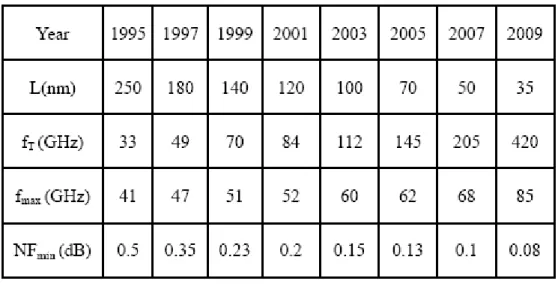
In the past 20 years, the silicon base MOSFET had widely been used in VLSI (Vary Large Scale Integration) applications. However, most RF circuits and systems have been implemented either compound semiconductor transistors. This is because that the microwave properties of silicon base MOSFET is inferior to other high-frequency transistors. In recent years, with the fast growth in the wireless communications market, the demand for high performance and low cost RF solutions is rising. Fortunately, the continuous down-scaling CMOS technology has resulted in a strong improvement in the RF performance of MOS device [5]. The basic structure of the MOSFET, shown in Fig. 1-1, consisting of a single gate, a semiconductor substrate and a heavily doped source and drain region, has not changed in the past twenty years. Only the dimensions and other features have been scaled down continuously to meet the demands of higher speed and increased compactness. There are several criterions to determine RF MOSFET performance such as cut-off frequency, maximum oscillation frequency, power gain, linearity, and noise figure. Table 1-1 shows the cut-off frequency, maximum oscillation frequency and minimum noise figure versus the gate length of n-channel MOSFET. For today, 50- to 100-nm gate length, the cut-off frequency and maximum oscillation frequency can achieve almost 200GHz and 70 GHz,
respectively. The NFmin for 70nm gate length RF MOSFET can be reduced to 0.13dB. In addition,
very high power gain (>25dB) is possible at realistic current for the most advanced technologies [6]. The VIP3 of 70nm gate length can be lower than 0.81V [7]. Therefore RF MOSFET has been serious alternatively to the traditional microwave transistors. Moreover, MOSFET offers very large scale integration and high reliability. As a result, to realize systems-on-chip, the RF operation must use RF MOSFET to conform to the integration.
1.3 Hot Carrier Reliability of RF MOSFET
With the scaling MOS transistor technology, the hot-carrier (HC) reliability becomes a challenging concern while keeping a relatively high drain voltage for both the digital and analog applications. Hot carrier generation and their effects in the characteristics of MOSFET have been known for a long time [8-10]. This results from high electric fields present inside the MOSFET which naturally appears when high biasing voltages are applied to a short-channel device. The general damages from the hot-carriers include the shift of the threshold voltage, the drain current degradation and the decreasing of transconductance. Because the RF circuits are sensitive to the parameters of their components [11], HC effects are also important in RF circuit design.
Table 1-1: Performance of CMOS technology in several generations
Chapter 2
Basic Theory and Experiments
2.1 Hot Carriers Mechanism
Hot Carriers result from the high electric fields inside the MOSFET when high biasing voltages are applied to a short-channel length device. Electrons in the inversion layer can get high energies in the high electric field. It is possible that carriers with high energy (i.e. hot carriers) have sufficient energy to overcome the potential barrier between the silicon and silicon dioxide and penetrate into the gate oxide. Some of the carriers may get stuck inside the gate oxide at the defect sites or traps, denoted by Nox. Hot carriers also can break the atomic bonds at the interface
of the silicon substrate and the gate oxide then generate new traps which called the interface traps. We denoted these traps by Nit. The difference between these two types of traps is that interface
traps can be in charge exchange with channel whereas the oxide traps cannot be in direct charge exchange with charges in the channel. These two types of traps will degrade the quality of gate oxide and affect the device electric parameters.
As shown in Fig.2-1(a), when the MOSFET is operated in the saturation region, the channel electrons will gain high energy on their way from source to drain and penetrate into gate oxide. The hot carriers are called channel hot electrons (CHE). The event of a carrier gaining energy and entering the gate oxide is a statistical phenomenon. The maximum numbers of hot carriers which penetrate into gate oxide occur when VG ≅VD [12]. Another effect that caused by energetic
generate new electron-hole pairs. These electron-hole pairs can also gain high energy in the electric field and produce new electron-hole pairs. This is similar to avalanche process in a reversed biased p-n junction and called drain avalanche hot-carriers (DAHC) (as shown in Fig.2-1(b). During the same process, the energetic carriers can impinge on the atomic bonds at the interface of the substrate and gate oxide or inside the oxide, and then break them. Therefore new electronic states Nit are created at the interface. In an NMOSFET, the extra electrons
generated in avalanche process are absorbed by drain, and the extra holes are absorbed by substrate terminal which form the substrate current component Isub. It is known that generation of
electron-hole pairs in an avalanche process is proportional to both strength of electric field and the number of primary carriers initially flowing in the channel. For low values of VG above the
threshold, the transistor is in deep saturation and a pinch-off region is formed near the drain which results in a strong lateral electric field in that region. Also, at low values of VG the drain
current is low. As VG increases, the drain current increases, but transistor comes out of saturation
region gradually. This causes that a maximum value for Isub appears at some particular value of
VG. It is reported that at VG ≅ 1
2VD the maximum Isub is generated in MOSFET [13].
The third mechanism of hot carriers is called substrate hot electrons (SHE). Unlike the cases in CHE and DAHC, which were caused by lateral electric field in the channel, SHE is caused by the vertical electric field between gate and the substrate. As shown in Fig 2-2(c), the electrons which are thermally generated in the region below the gate, drift toward the silicon-silicon dioxide interface and gain kinetic energy in the electric field below the gate. Some of these electrons penetrate into oxide and cause a uniform distribution of trapped charge in the oxide. SHE is not a major problem in short channel devices as compared to the long channel devices. Since most of the electrons are absorbed into source and drain region and a smaller fraction of
them reaches the device surface.
2.2 Oxide Breakdown Mechanism
Generally, in advanced MOS devices, there are two breakdown mechanisms observed in dielectric materials. First is called HBD (Hard-Breakdown) and has a permanently distortion in gate oxide dielectric. It results in a dramatic increase of the output currents due to the increasing gate leakage current. The other breakdown mechanism is called SBD (Soft-Breakdown), and the breakdown process shows smoothly and slightly. The physical mechanism involved in, and leading to, the dielectric breakdown process are very complex. They involve impact ionization in the oxide layer, injection of holes from the anode, creation of electron-hole pairs in the oxide, electron and hole trapping, creation of surface state at the oxide-silicon interface, and the interaction of many or all of these process.
The mechanism of tunneling into an electron trap can be explained by Fig.2-2(a). As electrons tunnel into an oxide layer, some of the electrons can get trapped. The trapped electrons modify the oxide field so that the field decreased near the cathode and increased near the anode. Hence the tunneling current will reach a stable value in Soft Breakdown.
As electrons travels in the conduction band of an oxide layer, it gains energy from the oxide filed. If the voltage drop across the oxide layer is larger than the band-gap energy of silicon dioxide, the electron can get enough energy to cause impact ionization. As shown in Fig.2-2(b), when a tunneling electron arrives to the anode, it could cause impact ionization in the anode near oxide-anode interface. Depending on the energy of the tunneling electron, the hole thus generated could be from deep down in the valence band, and thus could be “hot”. A hot hole in the silicon–oxide interface have a high probability of been injected into oxide layer. On the other
hand the injected hole can be trapped in the oxide layer as it travels towards the cathode.
The trapped holes in the oxide layer resulting in an increase in the oxide field near the cathode and a decrease in the oxide field near the anode (shown in Fig.2-2(c)). According to the F-N tunneling equations [14]:
J
FN = 3 3 2 4 2 * 2 exp( ) 16 3 ox ox ox ox q E m qE π Φ − Φ = =(2-1)
a small increase in the oxide field near the cathode can cause a large increase in the tunneling current. Thus, hole-trapping in oxide near the cathode provides positive feedback leading to the electron tunneling process. Dielectric hard breakdown occurs when the positive feedback leads to a run away of the electron tunneling current at some local weak spots of the oxide [15]. It appears as a current prominence in current-versus-time plots.
2.3 Device under Test and Measurement Techniques
2.3.1 Device under Test
The devices under test are n type MOSFETs in N-well. Multi-finger MOS transistors used in this work were fabricated using a 0.13μm baseline technology with channel length L= 0.13μm. In our structures, two cells are parallel and each cell have 16 fingers with fingers width LF= 4μm.
The gate oxide thickness is 22Å.
2.3.2 I-V Measurement
Agilent 4156B precision semiconductor parameter analyzer. The threshold voltage (Vth) and
transconductance (gm=dID/dVG) are extracted from the ID-VG curve.
2.3.3 High Frequency Characteristics Measurement
For microwave devices, the high frequency characteristics are generally obtained by the measurement of the s-parameters. In this work, on-wafer s-parameters measurement was carried out from 0.1 to 50.0 GHz using microwave coplanar probes and HP 8510C Network Analyzer. On-wafer dummy structures were used to de-embed the pad parasitics. Then, the de-embedded parameters were transformed to the H, Z or Y parameters to extract the desired parameters.
2.3.4 Output Power Measurement
We used the load-pull system (ATN LP1 measurement system) to measure and discuss power characteristics and linearity in our study. The functions of this load-pull system perform power discussions on output power, power gain, power added efficiency (PAE), and inter-modulation distortion. The configuration of a load-pull system is shown in Fig.2-3(a).
By load-pull test, the output power is measured and plotted as a function of the complex load seen by the transistor. Since a complex load requires two axes, the plot actually appears as constant power contours on a complex impedance plane, for example, a Smith chart. A variable, precisely calibrated tuner operates as a matching network, presenting various complex impedances to the transistor according to a control input. With the aid of an automated system, the real and imaginary parts of Z1 are gradually varied such that the power meter maintains a constant reading. The result is the contour corresponding to that power level shown in Fig.2-3(b). When Z1 arise so does Zin, necessitating the use of the tuner between the signal generator and the transistor to ensure that the impedance seen by the generator remains constant.
If the power delivered to the input is constant, the output power increases as Z1 approaches its optimum value, Zopt. This trend is accompanied by a narrower range for Z1, resulting in the tighter contours and eventually a single impedance value, Zopt, as the output reaches its maximum level, Pmax. In other words, the load-pull test systematically narrows downs the values of Z1 so as to obtain both the maximum output power and corresponding load impedance. The load pull system can also calculate intermodulation distortion using two-tone frequency test.
Fig. 2-1 (a)
Fig. 2-1 (b)
Fig. 2-1 (c)
Fig. 2-1 (a) Channel hot electrons (b) Drain avalanche hot carriers
(c) Substrate hot electrons
Fig. 2-2 (a)
Fig. 2-2 (b)
Fig. 2-2 (c)
Fig. 2-2 (a) Schematic illustrating the trapping of tunneling electrons.
(b) Schematic illustrating the generation of an electron-hole pair in the anode
by a tunneling electron.(c) Schematic illustrating the trapping of holes in
the oxide layer
Fig. 2-3 (a)
Fig. 2-3 (b)
Fig. 2-3 (a) Block diagram of the load-pull measurement system.
(b) Power contours on a Smith chart
Chapter 3
The DC & RF characteristics on RF power transistors
Introduction
In this chapter, a new structure named pseudo-drain MOS (PDMOS) [16] was introduced and investigated. PDMOS improves from a standard Drain-extended MOS (DEMOS). We also make some changes from PDMOS and compare their DC and RF characteristics. Although the BVDS in DEMOS is higher than in PDMOS, the speed and RF performance of the PDMOS is
better than that of the DEMOS.
3.1 Device Fabrication and Design
The structures under test were fabricated using a standard 0.13μm CMOS process with 22-nm-thick gate oxidation and twin-well technique. Without any additional mask, the device was designed by layout scheme as shown in Fig.3-1(b). The drawn geometry of a single-cell has 16 fingers with a 0.13μm gate length and 4μm gate width. For multi-cell design, 2 cells were parallel to reach higher output current and lower gate resistance.
The DEMOS which shown in Fig.3-1(a) was designed simply with an n-type well structure extending underneath the STI (0.12μm) to the internal drain region of the device adjacent to the actual poly gate. Due to the lateral diffusion caused by the successive thermal treatments inherent in the process, this relatively lower dose N-well (~1018cm-3) becomes a high resistance (n-) drift region and can be regarded as a “series-wound” connection between the channel and drain
diffusion region. This drift region acts as a drain-extended (DEMOS) as shown in Fig.3-1(a). In PDMOS, we added an N+ region to keep the lightly doping N-well extended drift region away from the channel. Therefore, the influence of the (n-) drift well region on the device channel region can be minimized. This is one of the key features of the device which improves the gm
significantly and resulting in a superior high frequency performance.
3.2 Compare with DC Performance
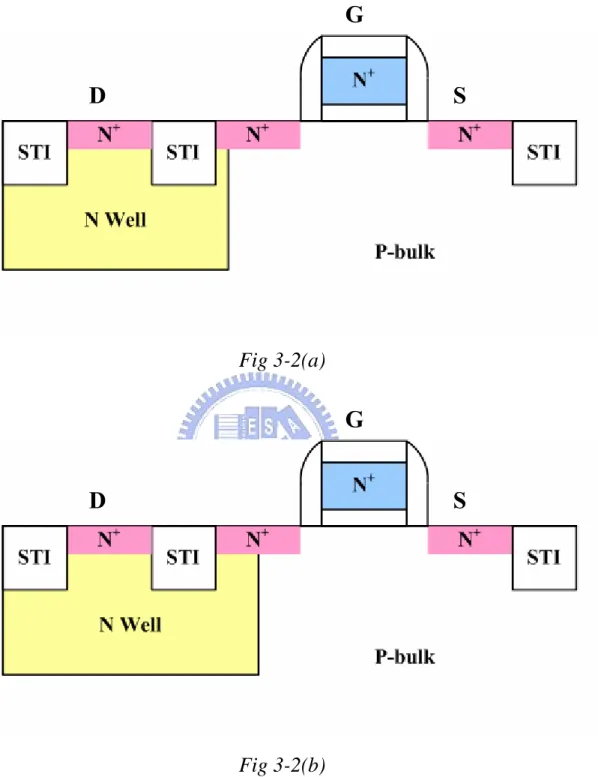
Two structures named HV01 and HV02 were discussed in this study. In HV01, the drawing N-well was located under the STI and drain (as shown in Fig.3-2(a)). In HV02, the N-well diffusion located Source diffusion to half (as shown in Fig.3-2(b)). Fig.3-3 shows the subthreshold characteristics of RF power PDMOS transistors with two different structures. Since the intrinsic gain of a transistor is highly depended on gm, the higher gm, the more attractive the
device is for analog/RF applications. In addition, it can be observed in Fig.3-3 that not only is the gm high for PDMOS, but the leakage current (Ioff) is also suppressed to a level as low as a
conventional core-NMOSFET. The low leakage current will result in lower power consumption when the PDMOS is in the off-state.
3.3 Compare with RF Performance
3.3.1 Experimental Procedures
High-Frequency characteristics were measured on chip using the HP8510 network analyzer from 20MHz to 50GHz. After de-embedding the parasitic pads effects, the current gain h21 was
calculated to extract the cutoff frequency (fT) which is one of the main figures-of-merit (FoM) of
(fmax), was also calculated and extrapolated from the maximum available gain (MAG). In this Pseudo-Drain MOS transistor, the gm is less influenced by extended drift region than in the DEMOS transistor, so that the high-frequency performance of fT (82GHz) is comparable to a
conventional 0.13μm NMOS transistor, and the RF performance on Pseudo-Drain MOS transistor is better than the Drain-extended MOS.
3.3.2 RF Performance
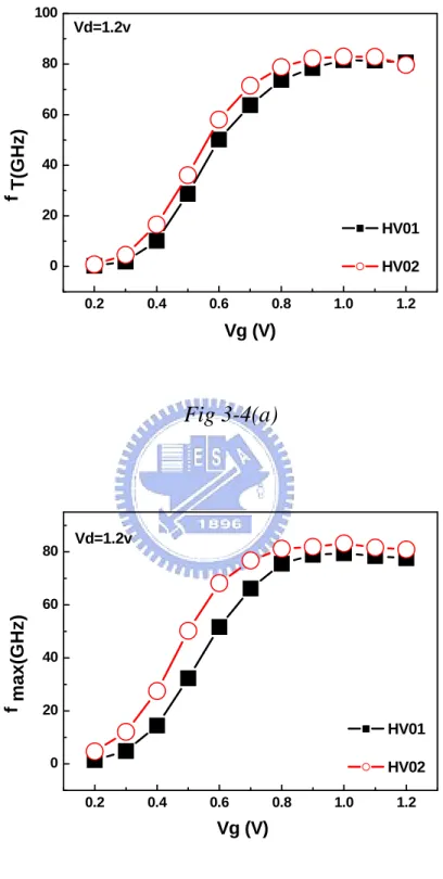
In this study, the bias dependences (fT) and (fmax) in our designed structures (HV01 and
HV02) are shown in Fig.3-4(a) and Fig.3-4(b). It was obvious in that picture that the gate biases at peak (fT) or (fmax) were different between HV01 and HV02. This was owing to the different
transconductance (gm) behaviors between them. And the HV02 exhibits higher fT and fmax than
those of the HV01 transistors with increasing stress time.
3.3.3 RF Power Performance
For RF power circuit design, fmax is the key FoM of a power transistor for high frequency
response. The fmax should be 5~10 times higher than the operation frequency of RF power circuits
and the parameters in a power device which influence fmax should be taken into account. Fig. Fig.
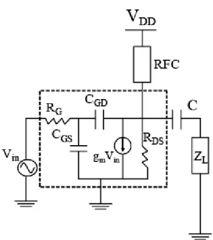
3-5 shows a typical power amplifier with an intrinsic device model. Using this schematic of a RF power amplifier, the dominant factors that influence fmax can be gleaned from the power gain vs.
frequency response equation corresponding to this model. The RF power gain is associated with the inherent current gain and the output impedance. When the source and load impedances are matched for maximum output power, the available power gain can be calculated and expressed as:
2 2 , max 4 (2 ) T G T G GD DS f Ga R f f R C R π = + (1)
where RG, CGD, RDS are gate resistance, gate-to-drain capacitance, and output resistance in the
device model. The comparison of the model parameters of HV01 and HV02 is summarized and listed in Table I. It was found that the better transconductance (gm) of the HV02 transistor was the
dominant factor contributing to the improvement of both the cutoff frequency (fT=gm/2πCgg) and
the maximum oscillation frequency. The RF power performance of the PDMOS transistor is also better than that of the HV02 as shown in Fig. 3-6. This is all due to the HV02 structure, in which the N-well diffusion located Source diffusion to half to let the drain current concentration higher. Fig. 3-6 shows the measured output power, power gain and power-added efficiency (PAE) of HV01 and HV02 under the bias condition of VG=1V and VD=1.2V, at a frequency of 2.4GHz,
and with the total width of 128μm at 2.4GHz. Using the load-pull system, which consists of HP85 122A and ATN LP1 (power parameter extraction software). The source and load impedances were tuned for maximum output power. For load-pull measurements, the operating frequency was chosen at 2.4GHz, a frequency commonly used in wireless communication. The maximum values of output power and power gain in this HV01 and HV02 structure can reach more than 11 dBm and 12 dB, respectively. The PAE, which gives an indication of the efficiency and power consumption, can also be 47% for the HV02 transistor compared to 45% for the HV01.
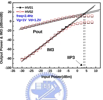
3.3.4 RF Linearity
RF linearity is also one of the major figures-of-merit of RF power characteristics. To characterize the linearity, the third-order intercept point (IP3), at which the output power and
third-order inter-modulation (IM3) power are equal to let it is commonly used. For low distortion operation, the third-order intercept point should be as high as possible. As shown in Fig.3-7, using a two-tone load-pull measurement, this HV02 shows an OIP3 value of 19 dBm at the bias of VG=1V and VD=1.2V. The OIP3 of HV02 is higher than that in HV01 (18.4dBm) and than in a
conventional DEMOS.
From the above experimental results, we found that the power performance of the ‘‘pseudo-drain’’ MOS transistors can meet the specifications of Bluetooth, wireless LAN, and other wireless applications.
3.4 Summary
A new power MOSFET design for RF power applications that relies on only layout scheme was investigated in this study. Without adding any masks and process modifications, a high breakdown voltage (BVDS) of 4.3V can be achieved in 0.13μm core-NMOS transistors. Because
the transconductance (gm) of HV02 is higher than HV01, the characteristics on DC or RF that
seems HV02 better than HC01. In addition, comparison of different CMOS power structures and with a raised biasing voltage was also addressed in this study. The results achieved from the implementation of 0.13μm MOS RF power devices demonstrate the potential power amplification capability of CMOS technologies for future integrated RF applications.
gm(ms) Rg(Ω) Cgg(fF) fT(GHz) fmax(GHz)
HV01 113.5 4.441 176.5 81 79.5
HV02 118.8 4.441 176 83 84
Table.3-1 Extracted model parameters of HV01 and HV02.
Device (@2.4G) DC Bias Condition Pout,max Gain(dB) PAE (%) Pout,1dB(dB) OIP3
HV01 VG=1V, VD=1.2V 11.5 15.2 45 8.19 18.4
HV02 VG=1V, VD=1.2V 12 15.8 47 8.54 19
G
Fig.3-1(a)
S
G
D
S
D
Fig.3-1(b)
Fig.3-1 Cross-sections of (a) Conventional "Drain-Extended" MOSFET, and (b)
"Pseudo-Drain"RF power MOS structure
G
Fig 3-2(a)
D
D
G
S
S
Fig 3-2(b)
Fig 3-2 (a) Schematic cross section of the HV01, and (b) Schematic cross
section of the HV02
0.0 0.2 0.4 0.6 0.8 1.0 1.2 10-9 10-7 10-5 10-3 10-1 0.00 0.02 0.04 0.06 0.08 0.10 0.12 VDS = 50mV, 1.2V VGS= 0 ~1.2 V GM (A /V ) ID(A) VG(V) HV01 HV02
0.2 0.4 0.6 0.8 1.0 1.2 0 20 40 60 80 100 Vd=1.2v f T(GHz) Vg (V) HV01 HV02
Fig 3-4(a)
0.2 0.4 0.6 0.8 1.0 1.2 0 20 40 60 80 HV01 HV02 Vd=1.2v f max(G H z ) Vg (V)Fig 3-4(b)
Fig.3-5 Simplified RF Power amplifier with an intrinsic RF small-signal model
-35 -30 -25 -20 -15 -10 -5 0 5 10 -20 -15 -10 -5 0 5 10 15 20 0 10 20 30 40 50 HV01 HV02 Ou tpu t Po wer & Power Gain (dB m /d B ) Input Power(dBm) freq=2.4Hz Vg=1V Vd=1.2V Power Ad ded Effici en cy(% )-35 -30 -25 -20 -15 -10 -5 0 5 10 -100 -80 -60 -40 -20 0 20 40 IIP3 IM3 Pout HV01 HV02 freq=2.4Hz Vg=1V Vd=1.2V O u tput Pow e r & IM3 (dBm/dB) Input Power(dBm)
Fig 3-7 Output power, and IM3 power as a function of input power for
Chapter 4
Characteristics of RF MOSFETs under Hot Carriers Stress
Introduction
In this chapter, the HC stress effects on DC and high frequency characteristics of RF MOSFETs will be discussed. In our experiments, the degradations are quite different by using different stress bias. We found that the degradations are more serious under drain avalanche hot carrier (DAHC) stress. After we discuss HC effects on the S-parameters, we found that the values of S22 and S21 are degraded seriously [17]. It implies that the output impedance and voltage gain
are influenced after stress. Finally, we focus on the changes of the main figures-of-merit (FOM) of RF MOSFETs after HC stress. It shows that the degradations of power characteristics are obvious due to the HC stress effect.
4.1 HC Stress Experiments
In our experiments, the channel length and total width of MOSFETs are 0.13μm and 128μ m, respectively. For DAHC stress, the gate and drain of the test transistors were biased at 1.5V and 3V, respectively. For channel hot electron (CHE) stress, the gate and drain of the test transistors were both biased at 3V. Finally, the third stress condition were biased at Vth+0.1V and
3V on gate and drain voltage, respectively. The DC characteristic and S-parameters were measured a fixed stress time that is terminated at 1000 second.
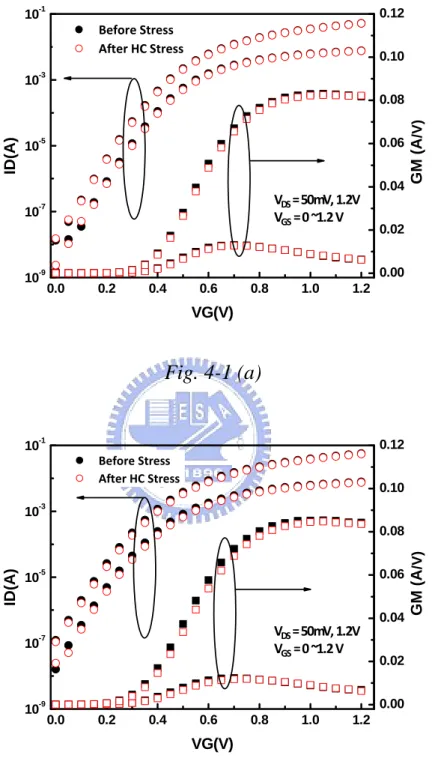
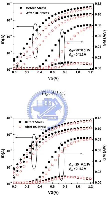
4.2 Effect of HC Stress on DC Characteristics
The general effects of the HC stress on the dc characteristics of HV01 and HV02 were showon in Fig.4-1. It shows unobvious variations for device under CHE stress as illustrated in Fig.4-1(a) and Fig.4-1(b). Therefore the channel hot electrons just slightly influence the DC characteristics of MOSFETs. On the contrary, it shows a large degradation for device measured after DAHC stress shown in Fig.4-1(c) and Fig.4-1(d). Hence the degradations caused by drain avalanche hot carriers are much larger compared to channel hot electrons. After DAHC stress, the degradation of saturation drain current in HV01 and HV02 are 14% and 14.2%, respectively. In Fig.4-1(c) and (d), the transconductance (gm) reduces significantly, and the maximum value shifts
to higher gate voltages after HC stress. We also found that gm and drain current reduction is more
serious in low gate bias region and this phenomenon is possibly due to the interface state generation and the oxide trap charge[18],[19].
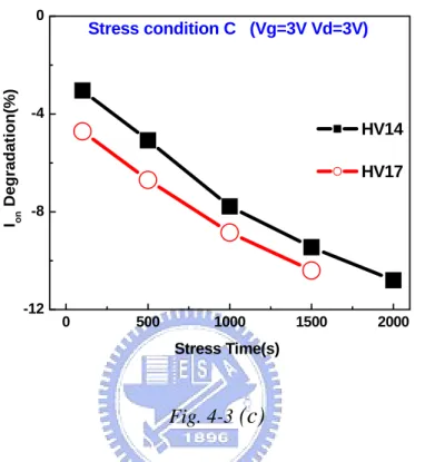
Now if we set to let gm degradation 10% and compare the two structure reliability. Figure.
4-2 describes the DC characteristics of these structures on three conditions. We can see obvious variation on condition C. This is because the drain resistance changes serious with high gate voltage. The I direction is analogue to g and it is show in Fig.4-3. Because the oxide traps larger electrons by
on m
drain avalanche hot-carriers (DAHC) than channel hot electrons (CHE), the Vth was raising obviously in Fig.4-4. Finaly, we noticed the Ron behaviors on these conditions
almost similar to the Vth. And that drawing is exhibition on Fig 4-5.
4.3 Effects of HC Stress on Cut-off Frequency and Maximum
Oscillation Frequency
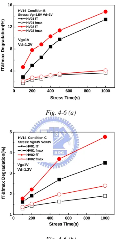
gain of a transistor with common source configuration and short-circuit load drops to unity. As shown in Fig.4-6, the cut-off frequency drops off conspicuously after HC stress. By using the small-signal equivalent-circuit model, the cut-off frequency (fT) can be approximated as:
2 ( ) m T gd gs g f C C π = + (4-1)
From above equation, fT is related with gm and gate-to-source capacitance (Cgs). After HC
stress, there are many interface states generated near the oxide and semiconductor interface. Therefore Cgs increased after stress. In addition, from discussions in Section.4-2, gm reduced
significantly after HC stress. Due to the increase of Cgs and the decrease of gm, fT reduced
dramatically after HC stress. By the observation of Fig. 4-6, it also suggested that the degradation of cut-off frequency is more robust to HC stress when biasing at higher gate voltages which is similar to the degradation of gm. Then we can find the degradation is serious on condition B. And
the HV02 structure has bad ability to against the hot-carrier stress. This characteristic is without reservation to show in the cut-off frequency.
As shown in Fig.4-6, maximum oscillation frequency (fmax) also decreases after HC stress.
The maximum oscillation frequency is defined as the transition frequency at which the unilateral gain of a transistor with common source configuration drops to unity. It can be approximated as: max 2 2 ) T T gd g ds in f f f C R G R π = + (4-2)
frequency, the degradations are correlated to the cut-off frequency. Therefore, fmax decreased after
HC stress and the degradation is more serious while biasing at low VG which is similar to the degradation of fT.
From Fig.4-6, we compared the RF performance degradation with the DC performance degradation. The degradations of fT and fmax are proportional to the gm degradation which can be
explained by equation (4-1) and (4-2). Comparing the slopes of these two lines in Fig.4-7, the degradation of fT is much larger than of fmax. Since fmax is proportional to the square of the gm, it is
less sensitive to HC stress.
4.4 HC Effects on Power Performance and Linearity
The effect of HC stress on the output power of a MOS transistor is shown in Fig.4-9. It was measured at gate voltage VGS=1 V and drain voltage VDS =1.2 V, where gm is the maximum value
in device saturation regions, and the frequency was operated at 2.4 GHz. The source and load impedances are matched for maximum output power before stress. The degradations of output power, power gain and power-added efficiency (PAE) are shown in Fig.4-9. The PAE can be expressed by: 1 (1 ) out in out DC DC P P P PAE P P − = = − G (4-3)
At low input power, the PAE is less changed under stress, due to the output power and drain current, and thus power dissipation, reduce simultaneously. When input power is larger than 1dB compression point, the degradations of PAE become serious. Because a part of the ac signal of drain current will be cut off as the input power is large enough. For this reason, the average drain current will increase with increasing input power. Since the bias current of the device after HC
stress is lower than that of the fresh one, the negative duty cycle of output waveform would enter the cut off region earlier. As a result, the power dissipation of stressed device is higher than that of fresh one, leading to lower PAE. Since the DC degradation is more serious after DAHC stress, the degradations of PAE is more serious after DAHC stress.
To characterize the linearity which is showed in Fig.4-10 that the third-order intercept point (IP3), at which the output power and third-order intermodulation (IM3) power are equal, is commonly used. For low distortion operation, the third-order intercept point should be as high as possible. From Table.4-1, we can take notice of the RF linearity degrades under DAHC stress is more serious than CHE stress when the MOSFET operates at a fixed gate bias.
4.5 Summary
Compared to HV01, although HV02 had better DC characteristic, the RF and power characteristics were weakly after the same stress condition. Therefore, we could say HV01 has better reliability than HV02. Also, we compared the identical device under the different stress conditions, the HC stress condition B had worse reliability to HC stress condition C on the same device.
IIP3 (dBm)
OIP3 (dBm)
Before Stress After stress Before Stress
After Stress
condition B
4.74
4.4
18.42
17.43
HV01
condition C
5.03
4.77
19.14
18.72
condition B
5.36
4.8
18.87
17.22
HV02
condition C
5.45
5.08
19.05
18.64
0.0 0.2 0.4 0.6 0.8 1.0 1.2 10-9 10-7 10-5 10-3 10-1 0.00 0.02 0.04 0.06 0.08 0.10 0.12 VDS = 50mV, 1.2V VGS= 0 ~1.2 V GM (A /V ) ID (A) VG(V) Before Stress After HC Stress
Fig. 4-1 (a)
0.0 0.2 0.4 0.6 0.8 1.0 1.2 10-9 10-7 10-5 10-3 10-1 0.00 0.02 0.04 0.06 0.08 0.10 0.12 VDS = 50mV, 1.2V VGS= 0 ~1.2 V GM (A /V ) ID (A) VG(V) Before Stress After HC StressFig. 4-1 (b)
Fig. 4-1: (a) DC characteristics of HV01 before and after CHE stress
(b) DC characteristics of HV02 before and after CHE stress
0.0 0.2 0.4 0.6 0.8 1.0 1.2 10-9 10-7 10-5 10-3 10-1 0.00 0.02 0.04 0.06 0.08 0.10 0.12 VDS = 50mV, 1.2V VGS= 0 ~1.2 V GM (A /V ) ID (A) VG(V) Before Stress After HC Stress
Fig. 4-1 (c)
0.0 0.2 0.4 0.6 0.8 1.0 1.2 10-9 10-7 10-5 10-3 10-1 0.00 0.02 0.04 0.06 0.08 0.10 0.12 VDS = 50mV, 1.2V VGS= 0 ~1.2 V GM (A /V ) ID (A) VG(V) Before Stress After HC StressFig. 4-1 (d)
Fig. 4-1: (c) DC characteristics of HV01 before and after DAHC stress
(d) DC characteristics of HV02 before and after DAHC stress
0 100 200 300 400 500 -12 -10 -8 -6 -4 -2 0 HV14 HV17 Stress condition A (Vg=Vth+0.1V Vd=3V) Stress Time(s) G m De gra d a tio n( % )
Fig.4-2 (a)
0 100 200 300 400 500 -12 -10 -8 -6 -4 -2 0 Stress condition B (Vg=1.5V Vd=3V) HV14 HV17 Stress Time(s) G m De gra d a tio n( % )Fig.4-2 (b)
Fig.4-2 (a) To compare gm characteristics of HV01 and HV02 on Condition A
with increasing stress time (b) To compare gm characteristics of HV01 and
HV02 on condition B with increasing stress time
0 500 1000 1500 2000 -12 -10 -8 -6 -4 -2 0 Stress condition C (Vg=3V Vd=3V) HV14 HV17 Stress Time(s) Gm Deg radati o n (% )
Fig.4-2 (c)
Fig.4-2 (c)To compare gm characteristics of HV01 and HV02 on
condition C with increasing stress time
0 100 200 300 400 500 -12 -8 -4 0 HV14 HV17 Stress condition A (Vg=Vth+0.1V Vd=3V) Stress Time(s) I on Degr adati o n (%) Fig. 4-3
(a)
0 100 200 300 400 500 -20 -16 -12 -8 -4 0 Stress condition B (Vg=1.5V Vd=3V) HV14 HV17 Stress Time(s) I on Degr adati o n (%) Fig. 4-3(b)
Fig. 4-3: (a) To compare Ion characteristics of HV01 and HV02 on
condition A with increasing stress time (b) To compare I
oncharacteristics
0 500 1000 1500 2000 -12 -8 -4 0 Stress condition C (Vg=3V Vd=3V) HV14 HV17 Stress Time(s) I on De g ra d a tio n( % ) Fig. 4-3
(c)
Fig. 4-3: (c) To compare I
oncharacteristics of HV01 and HV02 on
0 100 200 300 400 500 0.00 0.02 0.04 0.06 0.08 0.10 0.12 HV01 HV02 Stress condition A (Vg=Vth+0.1V Vd=3V) V th Degrada tion Stress Time(s)
Fig.4-4 (a)
0 100 200 300 400 500 0.00 0.02 0.04 0.06 0.08 0.10 0.12 Stress condition B (Vg=1.5V Vd=3V) HV01 HV02 Vth Degrada tion Stress Time(s)Fig.4-4 (b)
Fig.4-4 (a) To compare V
thcharacteristics of HV01 and HV02 on condition A
with increasing stress time(b) To compare V
thcharacteristics of HV01 and
0 500 1000 1500 2000 0.00 0.02 0.04 0.06 0.08 0.10 0.12 Stress condition C (Vg=3V Vd=3V) HV01 HV02 Stress Time(s) V th Degr adati on
Fig.4-4 (c)
Fig.4-4 (c) To compare V
thcharacteristics of HV01 and HV02 on
0 100 200 300 400 500 0 10 20 30 40 HV01 HV02 Stress condition A (Vg=Vth+0.1V Vd=3V) R on De g rad ati o n (% ) Stress Time(s)
Fig.4-5 (a)
0 100 200 300 400 500 0 10 20 30 40 Stress condition B (Vg=1.5V Vd=3V) HV01 HV02 R on De g rad ati o n (% ) Stress Time(s)Fig.4-5 (b)
Fig.4-5(a) To compare R
oncharacteristics of HV01 and HV02 on
condition A with increasing stress time (b) To compare R
oncharacteristics of HV01 and HV02 on condition B with increasing
0 500 1000 1500 2000 0 10 20 30 40 Stress condition C (Vg=3V Vd=3V) HV01 HV02 Stress Time(s) R on Deg radati on (% )
Fig.4-5 (c)
Fig.4-5 (c) To compare R
oncharacteristics of HV01 and HV02 on
0 200 400 600 800 1000 4 8 12 16 Vg=1V Vd=1.2V HV14 Condition B Stress: Vg=1.5V Vd=3V HV01 fT HV01 fmax HV02 fT HV02 fmax fT&fmax Degradation(%) Stress Time(s)
Fig. 4-6 (a)
0 200 400 600 800 1000 1 2 3 4 5 fT &fmax Deg rad atio n (%) Stress Time(s) HV14 Condition C Stress: Vg=3V Vd=3V HV01 fT HV01 fmax HV02 fT HV02 fmax Vg=1V Vd=1.2VFig. 4-6 (b)
Fig. 4-6: (a) Cut-off frequency before and after HC stress on HV01
and HV02 (b) Maximum oscillation frequency before and after HC
0 200 400 600 800 1000 4 8 12 16 Vg=1V Vd=1.2V HV14 Condition B Stress: Vg=1.5V Vd=3V HV01 fT HV01 fmax HV02 fT HV02 fmax fT&fmax Degradation(%) Stress Time(s)
Fig. 4-7 (a)
0 200 400 600 800 1000 1 2 3 4 5 fT &fmax Deg rad atio n (%) Stress Time(s) HV14 Condition C Stress: Vg=3V Vd=3V HV01 fT HV01 fmax HV02 fT HV02 fmax Vg=1V Vd=1.2VFig. 4-7 (b)
Fig. 4-7: (a) Cut-off frequency before and after HC stress on
HV01 and HV02 (b) Maximum oscillation frequency before and
after HC stress on HV01 and HV02
5 10 15 3 6 9 12 15 Vg=1v Vd=1.2v gm Degradation(%) fT& fmax Deg rad a ti o n (% ) HV01 Condition B Stress: Vg=1.5V Vd=3V fT fmax
Fig. 4-8 (a)
3 6 9 12 15 3 6 9 12 15 gm Degradation(%) fT& fm a x D e g rad ati o n (%) Vg=1v Vd=1.2v HV02 Condition B Stress: Vg=1.5V Vd=3V fT fmaxFig. 4-8 (b)
Fig. 4-8: (a) Relation between f
Tand f
maxdegradations and gm degradation on
condition B of HV01 (b)Relation between f
Tand f
maxdegradations and gm
2 3 4 1 2 3 4 Vg=1v Vd=1.2v gm Degradation(%) fT& fmax Deg rad a ti o n (% ) HV01 Condition C Stress: Vg=3V Vd=3V fT fmax
Fig. 4-8 (c)
2 3 4 5 1 2 3 4 5 Vg=1v Vd=1.2v gm Degradation(%) fT& fmax Deg rad a ti o n (% ) HV02 Condition C Stress: Vg=3V Vd=3V fT fmaxFig. 4-8 (d)
Fig. 4-8: (c) Relation between f
Tand f
maxdegradations and gm degradation on
condition C of HV01 (d) Relation between f
Tand f
maxdegradations and gm
-35 -30 -25 -20 -15 -10 -5 0 5 10 -20 -15 -10 -5 0 5 10 15 20 0 10 20 30 40 50
Output Power & Power G
a in (dB m /dB ) Input Power(dBm) Before stress After stress freq=2.4Hz Vg=1V Vd=1.2V Po wer Ad d ed Effi ci en cy(%) Fig. 4-9
(a)
-35 -30 -25 -20 -15 -10 -5 0 5 10 -20 -15 -10 -5 0 5 10 15 20 0 10 20 30 40 50 Out put Power & Power Gai n (dB m /d B ) Po wer Added Effi ci ency(%) Input Power(dBm) Before stress After stress freq=2.4Hz Vg=1V Vd=1.2V Fig. 4-9(b)
Fig. 4-9: (a) Output power, power gain and PAE versus input power before
and after HC stress on condition B of HV01. (b) Output power, power gain
and PAE versus input power before and after HC stress on condition B of
HV02
-Fig. 4-10 (a)
Fig. 4-10 (b)
Fig. 4-10: (a) Output power and 3
rd-order intermodulation (IM3) power
versus input power before and after HC stress on condition B of HV01
(b) Output power and 3
rd-order intermodulation (IM3) power versus input
power before and after HC stress on condition B of HV02
-35 -30 -25 -20 -15 -10 -100 -80 -60 -40 -20 0 20 40 5 0 5 10 IIP3 Before stress Pout IM3 After stress freq=2.4Hz Vg=1V Vd=1.2V O ut put P ow e r & IM3 ( dBm /dB) Input Power(dBm) -35 -30 -25 -20 -15 -10 -5 0 5 10 -100 -80 -60 -40 -20 0 20 40
IIP3
IM3
Pout
Before stress After stress freq=2.4Hz Vg=1V Vd=1.2V Out p utPower & IM3
(dBm
/dB)