國立交通大學
電信工程學系碩士班
碩 士 論 文
應用於超寬頻接收機之低電壓低功率低雜訊放大器
與多頻帶頻率合成器
Low-voltage, Low-power, LNA and Multiband
Frequency Synthesizer For UWB Receiver
研究生:張博揚
指導教授:周復芳 博士
應用於超寬頻接收機之低電壓低功率低雜訊放大器
與多頻帶頻率合成器
Low-voltage, Low-power, LNA and Multiband Frequency
Synthesizer For UWB Receiver
研究生:張博揚 Student:Po-Yang Chang
指導教授:周復芳 博士 Advisor:Dr. Christina F. Jou
國立交通大學
電信工程學系碩士班
碩 士 論 文
A thesis
Submitted to Department of Communication Engineering
College of Electrical and Computer Engineering
National Chiao Tung University
In Partial Fulfillment of the Requirements
For the Degree of
Master of Science
In Communication Engineering
June 2006
Hsin Chu, Taiwan, Republic of China
中 華 民 國 九 十 五 年 六 月
應用於超寬頻接收機之低電壓低功率低雜訊放大器
與多頻帶頻率合成器
研究生 : 張博揚 指導教授 : 周復芳 博士
國立交通大學電信工程學系碩士班
中文摘要
本論文的第一部份分三個方面研究超寬頻低雜訊放大器電路設計方法,包含輸入匹 配,雜訊指數和功率增益,並且以電路元件來表示這些特性。實作的超寬頻低雜訊放大 器顯示3.1 ~ 10.6GHz 具有小於-7.07dB 輸入返回損耗以及-12.5dB 輸出返回損耗,在 2.5 ~ 8.5GHz 具有 10dB 增益,3dB 頻寬約為 2 ~ 9 GHz,最小雜訊指數為 3.46dB,並且在 1V 的供給電壓下,放大器功率消耗為 7.25mW。 在第二部份,針對低相位雜訊設計一初始應用於超寬頻系統之頻率合成器,可分別 產生頻率8448MHz、4224MHz 和 2112MHz。利用 0.18 微米 CMOS 製程實現,於三頻 帶量測之相位雜訊小於-121dBc/Hz@1-MHz,可調頻寬約為 10%。於 1.8V 的供給電壓 下,總功率消耗為52.2mW。 此外,設計一應用於多頻帶正交分頻多工超寬頻系統之頻率合成器,從3 ~ 10GHz 具有 12 個可選擇頻帶,於此架構中,完成四相位壓控震盪器之模擬相位雜訊小於 -107dBc/Hz@1-MHz,可調頻寬為 7.93 ~ 10.3GHz。主要頻率輸出功率與旁路頻帶模擬 相差至少35dB。在 1.8V 的供給電壓下,核心電路消耗 81.1mW,緩衝器消耗 32.6mW。 模擬頻帶切換時間約為1ns。Low-voltage, Low-power, LNA and Multiband Frequency
Synthesizer For UWB Receiver
Student: Po-Yang Chang Advisor: Dr. Christina F. Jou
Institute of Communication Engineering
National Chiao Tung University
Abstract
In the first part of the thesis the design method of UWB LNA topology is studied and analyzed in three respects, including input matching, noise figure and power gain. These characteristics are expressed in terms of circuit elements. The implemented UWB LNA demonstrates S11 < -7.07dB and S22 < -12.5dB from 3.1 to 10.6 GHz. The power gain (S21) is 10dB from 2.5 to 8.5 GHz, the 3dB bandwidth is 2-9 GHz. The minimum noise figure is 3.46dB while consuming 7.25 mW with bias voltage of only 1V.
In the second part, an initial direct frequency synthesizer structure for UWB is designed with low phase noise performance, and three LO bands (8448MHz, 4224MHz and 2112MHz) are produced individually. Fabricated in 0.18-μm CMOS technology, in three LO bands, this work achieves the measured phase noise of less than -121dBc/Hz@1-MHz offset and the frequency tuning range of 10% while consuming 52.2mW from a 1.8-V supply.
Furthermore, a direct frequency synthesizer with 12 selective bands from 3 to 10 GHz is designed. In this prototype, we achieve QVCO’s simulated phase noise less than -107dBc/Hz@1-MHz offset and the tuning range from 7.92 ~ 10.3 GHz. The simulated output powers of twelve bands have better than 35 dB sideband rejection while consuming 81.1mW of the core circuit and 32.6mW of the buffer from a 1.8-V supply. The simulated switching time for hopping frequency is about 1ns.
Acknowledgement
首先,我要感謝指導教授周復芳老師,在這兩年來的指導和關心,讓我在碩士學業 求學過程獲益良多。並且要感謝高銘盛教授讓我對通訊領域有相當多的了解,引領我進 入通訊工程的大門,另外要感謝鄭國華學長的耐心教導,尤其當我遇到困難總能給我鼓 勵和協助,並且指引了我研究方向,讓研究更有目標。 還有要感謝實驗室的同學文明、政展、仕豪、秋榜、宏斌,和你們常常一起熬夜趕 作業和晶片下線,雖然辛苦,但是卻很開心在研究所生涯中能有一起共患難的朋友,另 外要感謝已畢業的學長欽賢、偉誠、政宏、家良、俊賢、柏達,你們認真的研究態度一 直是我們的榜樣,也教導我們許多知識與實用的技巧,感謝和學弟子豪、宇清、志鵬、 宜興、學妹瑞嫻、學長匯儀、顯傑,有你們陪我一起渡過這兩年的研究生生活,彼此在 學業和研究各方面相互砥礪和支持,帶給了我一段美好、難忘、也最充實的時光。 最後我要感謝我最愛的父母親和家人,在我想走的路上,一路給我最大的支持和包 容,讓我能順利地完成碩士學業。Contents
Chinese Abstract...I
English Abstract ... II
Acknowledgement... III
Contents...IV
List of Tables ...VII
List of Figures ... VIII
Chapter 1 Introduction ... 1
1.1 Background and motivation
...
11.2 Thesis organization
...
4Chapter 2 Low-voltage, Low-power, Low Noise Amplifier for UWB
Receivers ... 6
2.1 Introduction
...
62.1 Architectures
...
72.3 Design considerations
...
92.3.1 Input matching analysis
...
92.3.2 Noise analysis
...
152.3.3 Gain analysis
...
202.4 Chip implementation and measured results
...
212.4.1 Layout considerations...21
2.4.3 Measurement results and discussions...25
2.4.4 Comparisons ...33
Chapter 3 A 3-to-10-GHz Direct Frequency Synthesizer with 12 selective
bands for MB-OFDM UWB Communication ... 34
3.1 Introduction ...34
3.2 Building block of low phase noise design...36
3.2.1 Binary 8448MHz Voltage-Controlled Oscillator (VCO)...36
3.2.2 Frequency dividers ...41
3.2.3 Switched buffer...42
3.3 Chip implementation and measured results of low phase design...44
3.3.1 Measurement considerations ...44
3.3.2 Measurement results...46
3.3.3 Measurement discussions ...50
3.4 The architecture of the multiband frequency synthesizer...51
3.5 Building block of the multiband frequency synthesizer...53
3.5.1 Quadrature Voltage-Controlled Oscillator (QVCO)...53
3.5.2 Frequency dividers ...56
3.5.3 Wideband Quadrature Mixer ...57
3.5.4 Switched buffer...60
3.6 Post-Simulation results of multiband frequency synthesizer ...60
Chapter 4 Conclusions and future works ... 69
4.1 Conclusions ...69
4.2.2 Cognitive communications...72
Reference ... 75
List of Tables
Table 1.1.1 Power spectral densities of some common wireless broadcast and communication
systems ...2
Table 2.3.1 Element values for equal-ripple low-pass filter prototypes...12
Table 2.4.1 Performance summary of low-voltage, low-power LNA ...33
Table 2.4.2 The comparisons of this work and recent UWB LNA papers. ...33
Table 3.3.1 summaries of the simulation and measurement...50
Table 3.4.1 Plan of selective-band switches in the frequency synthesizer ...53
Table 3.6.1 Summary of wide tuning range QVCO ...66
Table 3.6.2 selective-band switches in the frequency synthesizer ...67
List of Figures
Fig. 1.1.1 Multiband spectrum allocation...3
Fig. 2.1.1 Block diagram of a UWB receiver...6
Fig. 2.1.2 Conventional distributed amplifier...7
Fig. 2.2.1 The fundamental architecture of the UWB LNA ...8
Fig. 2.3.1 The process of filter design by the insertion loss method...10
Fig. 2.3.2 Chebyshev (equal-ripple) low-pass filter response (N=3) ...11
Fig. 2.3.3 Ladder circuits for low-pass filter prototypes and their element definitions ...11
Fig. 2.3.4 Components convert from low pass filter to band-pass filter ...13
Fig. 2.3.5 Small signal equivalent circuit of the inductive source degeneration structure...13
Fig. 2.3.6 Basic schematic of the LNA input network ...14
Fig. 2.3.7 The whole schematic of the LNA input network ...14
Fig. 2.3.8 The Smith chart of the simulated return loss (S11) from 3.1 to 10.6 GHz ...15
Fig. 2.3.9 Noise model for the amplifying transistor M1...16
Fig. 2.3.10 Contour plots of the average NF ...19
Fig. 2.3.11 The schematic of UWB LNA...20
Fig. 2.3.12 Impact of parasitic capacitances...21
Fig. 2.4.1 Chip Photo of the UWB LNA...22
Fig. 2.4.2 The electromagnetic simulation and the inductance of Ls1...23
Fig. 2.4.3 On-wafer measurement test diagram...24
Fig. 2.4.4 Picture of on wafer measurement setup with four probes...24
Fig. 2.4.5 Measurement setup for (a) S-parameters (b) noise figure...25
Fig. 2.4.7 Measurement setup for third-order intercept point ...25
Fig. 2.4.8 Comparison between simulation and measurement of S11...27
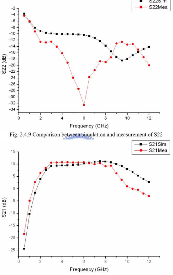
Fig. 2.4.9 Comparison between simulation and measurement of S22 ...28
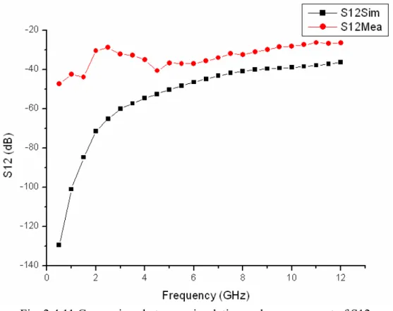
Fig. 2.4.10 Comparison between simulation and measurement of S21 ...28
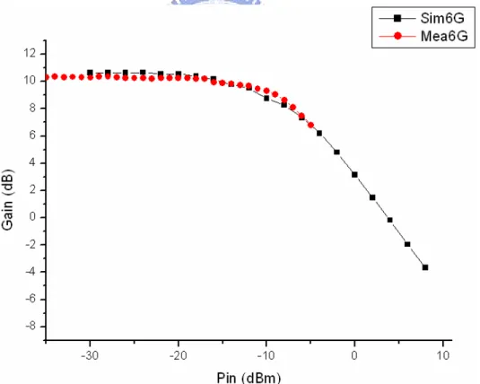
Fig. 2.4.11 Comparison between simulation and measurement of S12 ...29
Fig. 2.4.12 Comparison between simulation and measurement of noise figure...29
Fig. 2.4.13 Comparison between simulation and measurement of P1dB at 3 GHz ...30
Fig. 2.4.14 Comparison between simulation and measurement of P1dB at 6 GHz ...30
Fig. 2.4.15 Comparison between simulation and measurement of P1dB at 9 GHz ...31
Fig. 2.4.16 Comparison between simulation and measurement of IIP3 at 3 GHz ...31
Fig. 2.4.17 Comparison between simulation and measurement of IIP3 at 6 GHz ...32
Fig. 2.4.18 Comparison between simulation and measurement of IIP3 at 9 GHz ...32
Fig. 3.1.1 The prototype of the low phase noise design ...35
Fig. 3.1.2 Direct frequency synthesizer creating the twelve carrier frequencies...36
Fig. 3.2.1 Behavioral model of an ideal LC oscillator ...37
Fig. 3.2.2 Voltage controlled oscillator structure ...38
Fig. 3.2.3 Spiral inductor in this synthesizer (a) layout (b) equivalent circuit model ...40
Fig. 3.2.4 MOS varactor in this synthesizer (a) layout (b) equivalent circuit model ...40
Fig. 3.2.5 Block diagram of the 2-stage dividers ...41
Fig. 3.2.6 Circuit schematic of the D Flip-flop ...42
Fig. 3.2.7 Controlled switched buffer used to change the carrier frequency...42
Fig. 3.2.8 The simulated waveforms of three LO bands ...43
Fig. 3.2.10 The settling time of the frequency switching ...43
Fig. 3.2.11 The frequency response of the buffer...44
Fig. 3.3.1 Chip micrograph...45
Fig. 3.3.2 Measurement instruments ...46
Fig. 3.3.3 PCB layout of the frequency synthesizer ...46
Fig. 3.3.4 Output spectrum of FFT at (a) 8448 MHz (b) 4224MHz (c) 2112 MHz...48
Fig. 3.3.5 Measurement output spectrum at (a) 8448 MHz (b) 4224MHz (c) 2112 MHz ...48
Fig. 3.3.6 Measurement tuning range of (a) VCO (b) 1st divider (c) 2nd divider ...49
Fig. 3.3.7 Phase noise of the VCO in this synthesizer ...49
Fig. 3.3.8 Measurement phase noise at (a) 8448 MHz (b) 4224 MHz (c) 2112 MHz...50
Fig. 3.3.9 The skirt effect through dividers. ...51
Fig. 3.4.1 Direct frequency synthesizer creating the twelve carrier frequencies...52
Fig. 3.4.2 The frequency plan of the frequency synthesizer...52
Fig. 3.5.1 Two Interleaved VCO configuration ...54
Fig. 3.5.2 Quadrature VCO circuit architecture ...54
Fig. 3.5.3 MOS varactor in this synthesizer ...55
Fig. 3.5.4 Spiral inductor in this synthesizer ...55
Fig. 3.5.5 MIM capacitor in this synthesizer...55
Fig. 3.5.6 The tuning range of the QVCO ...56
Fig. 3.5.7 Block diagram of the frequency dividers ...57
Fig. 3.5.8 The timing diagram of the frequency deviders ...57
Fig. 3.5.9 Conceptual illustration of SSB mixers ...58
Fig. 3.5.11 Spiral inductor with center tap ...58
Fig. 3.5.12 Circuit schematic of the wideband quadrature mixer...59
Fig. 3.5.13 The output spectrum of the quadrature mixer mixing 2112 MHz and 4224 MHz.59 Fig. 3.5.14 Controlled switched buffer used to change the carrier frequency...60
Fig. 3.6.1 The layout of the multiband frequency synthesizer ...61
Fig. 3.6.2 Tuning ranges of the QVCO (TT, FF, and SS corner)...61
Fig. 3.6.3 Simulated phase noise at Vbank on/off (a) TT (b) FF (c) SS corner ...62
Fig. 3.6.4 The FFT simulation results of twelve bands ...63
Fig. 3.6.5 Signal transient analysis...65
Fig. 3.6.6 Simulated output frequency synthesizer in the time domain by controlling the switches ...66
Fig. 4.2.1 A basic PLL structure...71
Fig. 4.2.2 Illustrating the notion of dynamic spectrum-sharing for OFDM based on seven channels ...73
Chapter 1
Introduction
1.1 Background and motivation
By the rapid development and large demand of wireless communications, fully integrated monolithic radio transceivers are the most significant considerations for communication applications. The recent rapid growth of the wireless communication market inspires many people to research the concerned region with strong passion. Of such many developments, enhanced operating frequency of CMOS technology encourages the designer to implement single-chip RF-to-baseband systems with it instead of bipolar or GaAs. One of the important design goals of portable wireless systems is low power consumption for long battery life. CMOS technology satisfies the requirements of low power consumption, low cost, reduced size, and also a few gigahertzs operating frequency in wireless systems.
Historically, wireless communications have only used a narrow bandwidth and can hence have a relatively high power spectral density. Ultra-wideband (UWB) system is an emerging high-speed and low-power wireless communication approved by Federal Communication Commission (FCC) in 2002 for commercial applications in the frequency range from 3.1 to 10.6GHz. UWB performs excellently for short-range high-speed uses, such as automotive collision-detection systems, through-wall imaging systems, and high-speed indoor networking, and plays an increasingly important role in wireless personal area network (WPAN) applications. This technology will be potentially a necessity in our daily life, from wireless USB to wireless connection between DVD player and TV, and the expectable huge market attracts various industries.
UWB system, the pulses have a short time and very wide bandwidth. It is helpful to review some traditional wireless broadcast and communication applications and calculate their power spectral densities (PSDs) as shown in Table 1.1.1.
Table 1.1.1 Power spectral densities of some common wireless broadcast and communication systems
System UWB Radio Television 2G Cellular 802.11a Transmission Power (W) 1mW 20kW 100kW 10mW 1W Bandwidth (Hz) 7.5GHz 75kHz 6MHz 8.33kHz 20MHz Power spectral density (W/MHz) 0.013 666,600 16,700 1.2 0.05 Classification wideband narrowband narrowband narrowband widebandultra
The IEEE 802.15.3a task group [1] currently discusses the standardization for UWB systems. Two possible approaches have emerged to exploit the allocated spectrum. One is the so-called “impulse radio” with code division multiple access (CDMA) modulation, based on the transmission of very short pulses, with pulse position or polarity modulation. This kind of receiver [2] is all digital circuit except LNA and a mixer, and time domain should be also considered to design especially for mixer because the carrierless signals possess wide frequency-band and using short pulse means discontinuous signal. Another is multi-band approach, with fourteen 528-MHz sub-bands, orthogonal frequency division multiplexing (OFDM) modulation, and frequency-hopping technique. This kind of receiver [3] can reject the wireless local area network (WLAN) signals and other causes of interference, and the division of the UWB frequency spectrum into sub-bands is illustrated in Fig. 1.1.1.
Fig. 1.1.1 Multiband spectrum allocation
A low noise amplifier (LNA) determines the performance of the receiver in the both modulation techniques. It is widely used in front-ends of narrowband communication systems. For UWB applications these devices will play a slightly different role. In fact, the design of the UWB LNA is one of the biggest challenges, because it connects with the antenna and the pre-select filter, and the input matching should be 50Ω over the whole bandwidth. Furthermore, we also focus on the design and implementation of LNA for low-power, low-voltage UWB system with bias voltage of only 1V. This work is designed and processed using TSMC 0.18µm mixed-signal/RF CMOS 1P6M technology, where the measured S11 < -7.07dB and S22 < -12.5dB from 3.1 GHz to 10.6 GHz. The power gain (S21) is 10dB from 2.5 to 8.5 GHz, the -3dB bandwidth is 2-9 GHz. The minimum noise figure is 3.46dB while consuming 7.2 mW.
In the section of the frequency synthesizer, between the two modulation techniques, the multiband UWB has greater flexibility in coexisting with other international wireless systems and future government regulator, and could avoid transmitting in already occupied bands. The receiver of such a system should have high linearity and a wideband local oscillator (LO) capable of frequency hopping in less than 9ns. So, a direct frequency synthesizer structure with quadrature phases for UWB systems is presented. At first, an initial direct frequency synthesizer structure for UWB is designed with low phase noise performance. The circuit consists of a binary 8448MHz voltage controlled oscillator (VCO) and 2-stage frequency
dividers, and three LO bands (8448MHz, 4224MHz and 2112MHz) are produced individually. The switched buffer as multiplexer with symmetrical independent architecture is used to select output frequency and lowers the phase noise. Fabricated in 0.18-μm CMOS technology, in three LO bands, this work achieves the phase noise of less than -121dBc/Hz@1MHz offset and the frequency tuning range of 10% while consuming 52.2mW from a 1.8-V supply.
Furthermore, according to the front design, a fast-hopping frequency synthesizer that generates more LO signals of twelve bands from 3 to 10 GHz is designed. The prototype is completed by combining a wideband quadrature voltage-controlled oscillator (QVCO) from 7.93 to 10.3 GHz, 2-stage dividers, switched buffer and only one quadrature single-sideband (SSB) mixer. Fabricated in 0.18-μm CMOS technology, this work achieves QVCO’s simulated phase noise less than -107dBc/Hz at 1 MHz offset, and the simulated output powers of twelve bands have better than 35 dB sideband rejection while consuming 60.76mW of the core circuit and 52.93mW of the buffer from a 1.8-V supply. The simulated switching time for hopping frequency is about 1ns.
1.2 Thesis organization
This thesis discusses about the circuit design and implementation for Ultra-wideband applications. The contents consist of two major topics: “3.1~10.6GHz low-voltage, low-power, low-noise amplifier” and “a 3-to-10-GHz direct frequency synthesizer for MB-OFDM UWB Communications”, respectively in Chapter 2 and Chapter 3. We will present the design flow and experimental results in TSMC 0.18-μm CMOS process. Moreover, we will discuss the reasons of differences between simulation and measurement results.
In Chapter 2, we will present the design and implementation of a low-voltage, low-power LNA for UWB applications. We will discuss the configuration, wideband input/output matching, noise and linearity of LNA. Besides, electromagnetic simulated
software Sonnet is used to approach simulated results to practical circuited property.
In Chapter 3, we will present the design and implementation of multiband frequency synthesizer for UWB applications. This chapter includes two circuits. The first section is an initial frequency synthesizer structure for the low phase noise design, and the circuit can produce three LO bands (8448MHz, 4224MHz and 2112MHz). The second section presents the design and simulated results of a fast-hopping frequency synthesizer that generates clocks for twelve bands from 3 to 10 GHz. The proposed topology provides a simple efficient method of frequency synthesizer to create multiband LO signals.
Finally, we discuss our simulated and measurement results, self-criticisms of the shortcomings in specification, and future prospects in Chapter 4. The UWB receiver and the advanced transceiver structure for cognitive communications are described for future communications.
Chapter 2
Low-voltage, Low-power, Low Noise Amplifier for
UWB Receivers
2.1 Introduction
A UWB receiver, diagrammed in Fig. 2.1.1, will feature a low-noise amplifier (LNA) followed by a correlator that removes the carrier from the received radio frequency (RF) signal. Analog-to-digital conversion will then allow for digital signal processing aimed at recovering the information data. In this chapter, it is clear that, regardless of what the future standard will be, a wideband LNA operating over the entire 7.5-GHz band of operation is required. Such an amplifier must feature wideband input matching to a 50-Ω antenna for noise optimization and filtering of out-of-band interferers. Moreover, it must show flat gain over the entire bandwidth, good linearity, minimum noise figure (NF) and low power consumption.
Fig. 2.1.1 Block diagram of a UWB receiver
Several CMOS LNA design techniques had been reported for broadband communication applications. The well-developed distributed amplifier is known as its excellent performance of gain-bandwidth product. However, as shown in Fig. 2.1.2, it requires several area consuming inductors to perform signal delay and many stages to provide a given gain that
consumes much power [4-5]. In other work, a cascode configuration [6] is used to achieve good performance with less number of active elements and power. Therefore, we will introduce the cascode structure and focus on the design and implementation of LNA for low-power, low-voltage UWB system. Besides, the electromagnetic effect of transmission lines is considered to minimize the difference between measured and simulated results in the improved LNA circuit.
Fig. 2.1.2 Conventional distributed amplifier
2.1 Architectures
The fundamental architecture of the UWB LNA is shown in Fig. 2.2.1. A cascode configuration with source inductive degeneration is used for the requirement of low power consumption. The cascode structure also has good properties of better reverse isolation, frequency response, lower noise figure and less Miller effect. [8-9]. To get flat gain performance over wide bandwidth, serial resistor Rd is used to improve the gain at low frequency.
In order to achieve wideband input matching from 3.1 to 10.6 GHz, the three-section Chebyshev filter is usually used in the input matching network by combining the gate-drain parasitic capacitance of M1 and the inductance Ls. In the conventional design, a capacitor is
usually added in parallel with the gate-drain parasitic capacitance to help design flexibility. In our design, we will try to simplify input matching network, and still maintain the wideband matching.
Fig. 2.2.1 The fundamental architecture of the UWB LNA
The noise performance of the proposed topology is determined by two main contributors: the losses of the input network and the noise of the amplifying device M1. The noise contribution of the input network is due to the limited quality factor Q of the integrated inductors. Its optimization relies on achieving the highest Q for a given inductance value, but it is limited by the wideband requirement of inductances that must be low-Q characteristic. Therefore, the optimization of the noise contribution from M1 is important and needs to extend the analysis to the wideband case. Finally, the size of M1 is determined.
An output-matching buffer is designed to achieve flat gain over the whole bandwidth and generate more output current. Unlike common source amplifier, the common drain structure is designed to supply current gain in high frequency. The size of M3 and the type of current source will determine the high-frequency characteristic of UWB LNA.
bandwidth, low noise and enough power gain while keeping low power dissipation will be discussed in the next section where a low power UWB LNA topology is presented.
2.3 Design considerations
2.3.1 Input matching analysis
The technique of filter design is employed for wideband input impedance matching. The two kinds of the most common used filter design technique are image parameter method and insertion loss method. The first one, image parameter method, consists of a cascade of simpler two-port filter sections to provide the desired cutoff frequencies and attenuation characteristics. Thus, although the procedure is relatively simple, the design of filters by image parameter method must often be iterated many times to achieve the desired results and that will result in large chip area. The other one, insertion loss method, uses network synthesis techniques to design filters with a completely specified frequency response. The design is simplified by beginning with low-pass filter prototypes that are normalized in terms of impedance and frequency. Transformations are applied to convert the prototype designs to the desired frequency range and impedance level [9]. The insertion loss method is used to design the broadband input matching for diminishing the implement costs. The Butterworth (Maximally flat) and Chebyshev (Equal ripple) filter design are two familiarly practical filter responses by used insertion loss method. The Butterworth design offers a smooth response curve with maximal flatness at zero frequency. The Chebyshev design offers a steeper response curve at the 3 dB cutoff frequency and requires fewer components. In this work, to have precipitous response curve at 3 dB cutoff frequency, the Chebyshev filter design is chosen. The filter designs can be scaled in terms of impedance and frequency, and converted to bandpass characteristics. This design process is illustrated in Fig. 2.3.1.
Fig. 2.3.1 The process of filter design by the insertion loss method The filter response is defined by its insertion loss, or power loss ratio, PLR:
2 ) ( 1 1 ω Γ − = = load inc LR P P P (2-1)
where Pinc is power available from source, and Pload is power delivered to load. Γ(ω)2 is an
even function of ω; therefore it can be expressed as a polynomial in ω2. Thus
) ( ) ( ) ( ) ( 2 2 2 2 ω ω ω ω N M M + = Γ (2-2)
where M and N are real polynomials in ω2. Substituting this form to (2-1) gives the following:
) ( ) ( 1 2 2 ω ω N M PLR = + (2-3)
Thus, for a filter to be physically realizable its power loss realizable its power loss ratio must be of the form in (2-3). Notice that specifying the power loss ratio simultaneously constrains the reflection coefficient, Γ(ω).
In this design, the Chebyshev polynomial is used to specify the insertion loss of an N-order low-pass filter as ) ( 1 2 2 c N LR k T P ω ω + = (2-4)
The passband response will have ripples of amplitude 1+k2, as shown in Fig. 2.3.2, since TN(x) oscillates between ±1 for |x|≦1. Thus, k2 determines the passband ripple level.
Fig. 2.3.2 Chebyshev (equal-ripple) low-pass filter response (N=3)
From the power loss ratio equation of Chebyshev filter, the normalized element values of L and C of low-pass filter prototypes is shown in Fig. 2.3.3, and the normalize values are listed in Table 2.3.1.
(a)
(b)
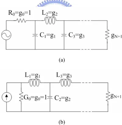
Fig. 2.3.3 Ladder circuits for low-pass filter prototypes and their element definitions. (a) Prototype beginning with a shunt element. (b) Prototype beginning with a series element.
Table 2.3.1 Element values for equal-ripple low-pass filter prototypes (g0=1, ωc=1, N=1 to 3, 0.5dB ripple) [10] N g1 g2 g3 g4 1 0.6986 1.0000 2 1.4029 0.7071 1.9841 3 1.5963 1.0967 1.5963 1.0000
Low-pass prototype filter designs can be transformed to have the bandpass response. If ω1
and ω2 denote the edges of passband, then a bandpass response can be obtained using the
following frequency substitution:
⎟⎟ ⎠ ⎞ ⎜⎜ ⎝ ⎛ − Δ = ⎟⎟ ⎠ ⎞ ⎜⎜ ⎝ ⎛ − − ← ω ω ω ω ω ω ω ω ω ω ω ω 0 0 0 0 1 2 0 1 (2-5) where 0 1 2 ω ω ω − =
Δ is the fractional bandwidth of passband. The center frequency, ω0, could
be chosen as geometric mean of ω1 and ω2, i.e.ω0 = ω1ω2 . The low-pass prototype transfers
to the band-pass filter type. The elements based on Table 2.1 are converted to series or parallel resonant circuits. The series inductor, Lk, is transformed to a series LC circuit with element
value: 0 ω Δ = ′ k k L L (2-6) k k L C 0 ω Δ = ′ (2-7)
The shunt capacitor, Ck, is transformed to a shunt LC circuit with element value:
k k C L 0 ω Δ = ′ (2-8) 0 ω Δ = ′ k k C C (2-9)
Fig. 2.3.4 shows the complete transformation circuit of low-pass filter converted to band-pass filter.
Fig. 2.3.4 Components convert from low pass filter to band-pass filter
Fig. 2.3.5 Small signal equivalent circuit of the inductive source degeneration structure In Fig. 2.3.5, since the input impedance of the MOS transistor with inductive source degeneration can be seen as a series RLC circuit
s T gs g s in L C s L L s s Z = + + +ω ) ( 1 ) ( ) ( (2-10)
where Cgs is the gate-source capacitance of M1, and ωT= gm / Cgs. The input matching network
of our third-order Chebyshev L-C filter structure can then absorb this MOS input impedance into its network. The size of M1 determines not only third-order L-C tank of band-pass filter but also the noise performance. According to these basic formulas, the models of authentic inductor and capacitor, and trading off noise performance, we can then omit the capacitor C2’
that shunts with the inductor L2’, and the capacitor C3’ is wholly replaced by the capacitance
Cgs of M1 without connecting additional capacitor, as shown in Fig. 2.3.6 [11]. The inductor
L3 is replaced by the inductors Lg and Ls. Besides, because the frequency of input signal is up
to 10GHz, the electromagnetic effect of transmission lines changes the characteristic of the input matching network. The effect of transmission lines between components is considered and simulated by the software, Sonnet. The whole input matching network is shown in Fig. 2.3.7. The block of S2P vin means the equivalent S-parameter model of the transmission line
between input node and the inductor L1. The block of S2P net01 means the equivalent
S-parameter between the inductor L1 and the capacitor C1, and so on. The capacitor Cpad is the
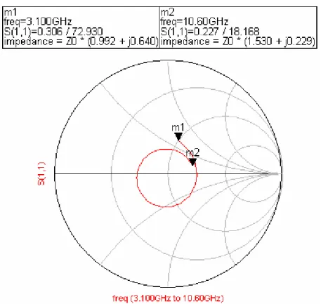
parasitic capacitance from the RF signal pad to ground. Therefore, the input network has lower complexity and good reflected coefficient from 3.1GHz to 10.6GHz. The Smith chart of the simulated return loss (S11) from 3.1 to 10.6 GHz is shown in Fig. 2.3.8.
Fig. 2.3.6 Basic schematic of the LNA input network
Fig. 2.3.8 The Smith chart of the simulated return loss (S11) from 3.1 to 10.6 GHz
2.3.2 Noise analysis
The noise performance of the proposed topology is determined by two main contributors: the losses of the input network and the noise amplifying device M1. The noise contribution of the input network is due to the limited quality factor Q of the integrated inductors. Its optimization relies on achieving the highest Q for a given inductance value. The optimization of the noise contribution from M1 relies instead on the choice of its width for a given bias current. Optimum device width has been fully discussed in the literature in the case of narrow-band LNA design [12]. The noise analysis of the wideband case is the optimization of the performance on the in-band average NF, as opposed to the NF at a single frequency. The analysis follows the guidelines of [14] in a dual fashion and with the difference that the loading effect of the local feedback inductor is taken into account. MOS transistor noise sources, shown in Fig. 2.3.9(a), are input-referred in a conventional way and replaced with two correlated noise generators, as shown in Fig. 2.3.9(b):
(a) (b)
Fig. 2.3.9 Noise model for the amplifying transistor M1 (a) M1 noise sources (b) input-referred equivalent noise generators.
nd m gs ng n i g C j i i = + ω (2-11)
(
)
sn m nd m nd s gs ng s n j Li g i g i L C i L j e = ω + 1−ω2 = + ω (2-12) where ind is the drain noise current, due to the carrier thermal agitation in the channel, whileing is the induced gate noise, due to the coupling of the fluctuating channel charge into the
gate thermal. The induced gate noise and drain current noise power spectral densities are, respectively
( )
0 2 2 5 4 d gs i g C kT S ng ω δ ω = (2-13)( )
4 d0 i kT g S nd ω = γ (2-14)where δ ≈ 1.33-4, and γ ≈ 0.67-1.33 are excess noise parameters [13], and gd0 is the channel
conductance at VDS=0.
The noise voltage en can be expressed as the sum of two components, one fully correlated,
enc, and the other, enu, uncorrelated to the noise current as follows: nu
nc n e e
e = + (2-15)
( )
( )
αχ χ α αχ ω αχ χ α αχ ω ω ω c c C j c c C L jX jX R S S Z gs gs s c c c i i e c n n n + + + ⋅ + + + ⋅ − = = + = = 1 2 1 1 2 1 1 2 2 2 2 2 (2-16) where χ = δ/(5γ), and( )
ω( ) ( )
ω ω nd ng nd ngi i i i S S Sc= / is the correlation coefficient between the gain noise and the drain noise. For MOS devices, the value of c is ≈ j0.4. The parameter
0
/ d m g
g =
α accounts for short-channel effects. It describes the transconductance reduction due to velocity saturation and mobility decrease due to the vertical fields.
The two uncorrelated noise sources, enu and in, are described by means of the following
parameters:
( )
( )
2 2 2 2 2 0 2 1 2 1 4 αχ α χ χ α α γ ω + + − ⋅ = = c c g kT S R d e u nu (2-17)( )
2 2(
2 2)
0 2 1 2 4 α ω αχ α χ γ ω + + ⋅ = = C c g kT S G gs d i n n (2-18) respectively.By using the introduced parameters, the NF can be expressed by
s n s c u R G Z Z R F 2 1+ + + = (2-19)
where Zs =Rs+ jXs is the source impedance.
Class noise optimization theory [13], shows that the minimum NF is achieved if the source impedance Zs =Zopt =Ropt+ jXopt is chosen such that
(
2 2)
2 2 2 1 1 χ α αχ ω αχ + + − = = + = c C c G R R G R R gs n u c n u opt (2-20)where, in this caseRc =0, and
c opt X
X =− (2-21)
resonates the series combination of Cgs and Ls. As a consequence, nearly minimum NF is
achieved over the entire amplifier bandwidth by using the proposed input network, which produces Xopt over a wide bandwidth. As a result of the foregoing discussion, the NF of the
LNA is
( )
( )
α γ ω ω ≈ + + = + ⋅ s m s n s u R g P R G R R F 1 1 (2-22) where( )
( )
2 2 2(
2 2)
2 2 2 2 2 2 1 2 1 1 ω αχ α χ χ α αχ χ α ω + + + + + − = C R c c c P gs s (2-23)Equations (2-22) and (2-23) show that, as α≦ 1 and χ < 1, using a smaller transistor for a given gm, i.e., drawing more current, is preferable. Moreover, increasing the transconductance
improves the noise performance, with all of the other parameters being the same.
The LNA NF described by (2-22) depends on three of the following four quantities: the drain bias current ID, the over-drive voltage Vod, the transistor width W, and the frequency. In
order to perform an optimization over the entire band of interest, the average NF must be considered. According to [6], Fig. 2.3.10 shows the contour plots of the average NF as a function of ID and W. For each value of the bias current, the device width can be chosen to
Fig. 2.3.10 Contour plots of the average NF [6]
In order to minimize the average NF, the more drain bias current ID has the better NF
performance, but it consumes more power. Therefore, in the condition of fixing the power consumption, decreasing the supply voltage and increasing the current can improve NF performance. Therefore, the supply voltage in this design is set a low voltage of 1V. The best average noise performance is achieved if 200 μm < W < 400 μm. Note that quantitative results of Fig. 2.3.10 only refer to the noise contribution of M1. Moreover, note that the NF decreases with the scaling of MOS technology. The NF in an actual LNA implementation is thus expected to be worse because of:
1. the losses of the input network, i.e., the limited quality factor of the integrated inductors;
2. the cascode device (M2) noise contribution, particularly significant at higher frequencies;
3. the load resistance (Rd) noise contribution;
2.3.3 Gain analysis
A single-cascode configuration with source inductive degeneration is used for improving the reverse isolation, frequency response, better noise figure and lower Miller effect. It also provides low-power characteristic at low supply voltage. The whole circuit of UWB LNA is shown Fig.2.3.11.
Fig. 2.3.11 The schematic of UWB LNA
At upper frequency, the transistor’s behavior is like a current amplifier. The current gain isβ
( )
s =gm/sCgs, and the current into M1 is Vin⋅W( )
s /Rs, where W(s) is Chebyshev transferfunction. Therefore, the voltage gain is
[
d d c]
s gs m in out R sL C R sC s W g V V // ) ( ) ( ⋅ + − = c d c d d d d s gs m C L s C sR R sL R R sC s W g 2 1 ) / 1 ( ) ( + + + ⋅ − = (2-23)where the combined capacitor Cc =Cdb2 +
[
CpassCgd3/(Cpass+Cgd3)]
, Cdb2 is the drain-body capacitance of M2, and Cgd3 is the gate-drain capacitance of M3. Equation (2-23) shows thatthe current gain roll-off is compensated by Ld. Moreover it shows that Cc introduces a
spurious resonance with Ld, which must keep out-of-band.
The total parasitic capacitance at the drain of M1 (sum of Cdb1 and Cgs2) introduces a pole
its source, the performance of the amplifier is improved, as shown in Fig. 2.3.12.
Fig. 2.3.12 Impact of parasitic capacitances
In this way, the capacitance between the source and the bulk of M1 is shorted, and Cdb1 is
connected between the drain and the source of M1. This decreases the contribution of Miller effect from Cdb1 and the total capacitance at the drain node at high frequency. This results in
an enhancement of the bandwidth of amplifier.
The source–follower buffer (M3 in Fig. 2.3.9) is needed to drive an external low-impedance load. The external output voltage V ′ is related to the output voltage of the out
amplifier by 3 2 2 / 1 m s s out out g sL sL V V + = ′ (2-24) The buffer is designed to improve the power gain of the amplifier at high frequency. The inductance Ls2, as a current source, biases the buffer and is simulated as a matching element to
maintain high gain at upper frequency. As a consequence, we can achieve the flat gain between 3.1-10.6GHz.
2.4 Chip implementation and measured results
2.4.1 Layout considerations
The chip photo of the UWB LNA is shown in Fig. 2.4.1. The layout skill is very important for radio frequency circuit design because it may affect circuit performance very much. In
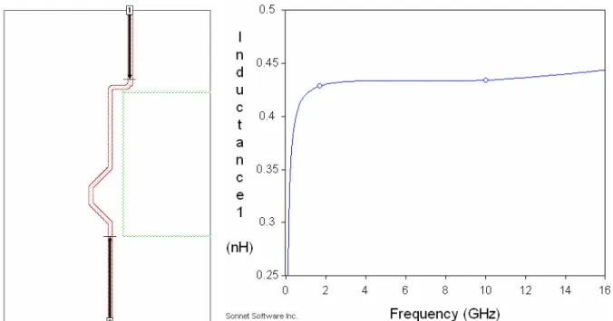
order to reduce noise that is considered in Section 2.3.2, the MOSFET is used as multi-finger, which total width is 320 μm, and the power supply (Vdd) is 1V. The 0.18μm (minimum) gate length was chosen to get the highest speed. The MIM (Metal-Insulator-Metal) capacitors without shield (the capacitance of per unit area) and hexagonal spiral inductors (the Q-value is below 18) are used in this work. Because the inductance of Ls1 is small, it is wholly replaced by a transmission line, and the inductance is 0.43nH, as shown in Fig. 2.4.2. The poly without silicide resistance is used for gate bias. Guard-rings are added with all elements to prevent substrate noise and interference. A shielded signal GSG pad structure is used in RF input and RF output to reduce the coupling noise from the noisy substrate. As for the connection lines, the power lines are considered for the current density while the signal lines are designed as short as possible. All interconnections between elements are taken as a 45° corner. The RF input and the RF output are placed on opposite sides of the layout to avoid the signals coupling. The chip size is 0.86 mm x 0.9 mm.
Fig. 2.4.2 The electromagnetic simulation and the inductance of Ls1
2.4.2 Measurement considerations
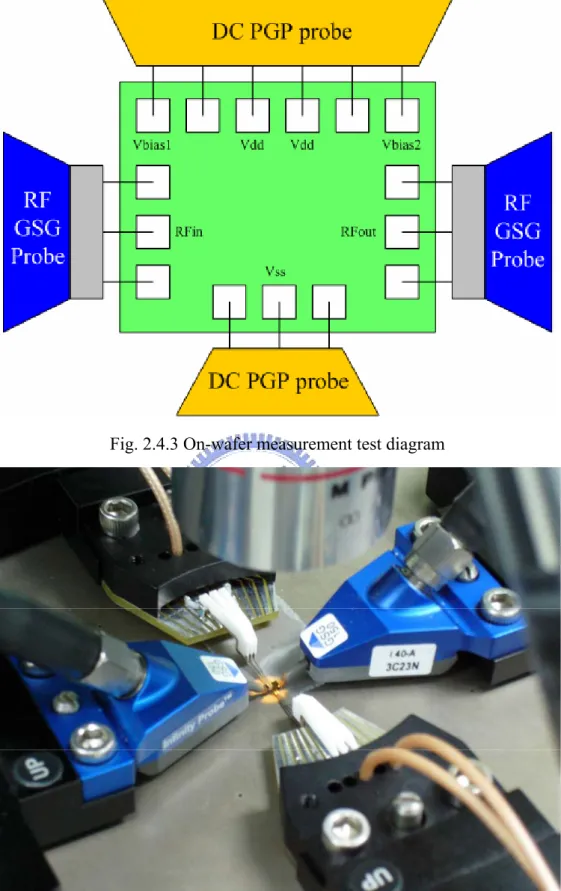
The UWB LNA is designed for on-wafer measurement so the layout must follow the rules of CIC’s (Chip Implementation Center’s) probe station testing rules. This circuit needs one 3-pin DC PGP probe, one 6-pin DC PGP probe and two RF GSG probes for on-wafer measurement. Fig. 2.4.3 shows the on-wafer measurement setup with four probes. The top and bottom probes are DC PGP probes which provide the power supply voltage and bias voltage for the circuit. The left and right probes are RF GSG probes.
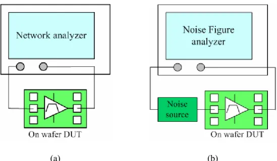
A large coupling capacitor is needed in the input of the UWB LNA to isolate the dc between circuit and equipment. Fig. 2.4.4 is the picture of the on-wafer measurement setup with four probes. Fig. 2.4.5 ~ Fig. 2.4.7 show the measurement setup for S-parameters, noise figure, 1dB compression point and third-order intercept point. We use the RF IC measurement system powered by LabView to measure the linearity of the UWB LNA. We will discuss the experimental and testing resultsof this circuit in following sections.
Fig. 2.4.3 On-wafer measurement test diagram
(a) (b) Fig. 2.4.5 Measurement setup for (a) S-parameters (b) noise figure
Fig. 2.4.6 Measurement setup for 1 dB Compression Point
2.4.3 Measurement results and discussions
This work is designed and processed using TSMC 0.18µm mixed-signal/RF CMOS 1P6M technology. The S-parameter are shown in Fig. 2.4.8 ~ Fig. 2.4.11, where the measured S11 < -7.07dB and S22 < -12.5dB from 3.1 GHz to 10.6 GHz. The power gain (S21) is around 10dB from 2.5 to 8.5 GHz, the 3dB bandwidth is 2-9 GHz. The measured noise figures show a good agreement. The minimum noise figure is 3.46dB at 5.46 GHz, and noise figure is at least less than 5.6dB from 3 to 9 GHz. The measured P1dB are -8.5dB at 3 GHz, -9.5dBm at 6 GHz, and
-8.5dBm at 9 GHz in Fig. 2.4.12 ~ Fig. 2.4.15. The measured IIP3s are 1dBm at 3 GHz, -2.5dBm at 6 GHz, and -2dBm at 9 GHz in Fig. 2.4.16 ~ Fig. 2.4.18. The measured results reveal the fact that the most difficult part of the design is to provide a flat gain up to 10 GHz. When high-frequency signal inputs, the power loss from the parasitic capacitance to the substrate is critical. For example, the combined capacitor Cc in equation (2-23) influences the
power gain, and the gate-source capacitance of M2 also offers a path of the power loss at high frequency. Besides, because the value of the inductor Ls1 is designed very small, the process variation has larger effect on this inductance. In this circuit, the inductance Ls1 made with a transmission line is smaller than it is designed. That induces the decreasing of the return loss and the increasing of the power gain. The modified simulation gives us a reasonable explanation the difference between simulation and measurement.
The measurement results reveal that the matching network of the UWB LNA is not as well as initial simulated results. That is because the process variation of devices. Although the physical models of the spiral inductors and MIM capacitors provided by the foundry were used in the simulation, only some certain size of the spiral inductors are measured and fitted. For example, the spiral inductor of W=15um, S=2um, R= 30um, 60um, 90um, 120um, and N=1.5, 3.5, 5.5 where W is the inductor track width, S is the spacing between tracks, R is the inner radius, and N is the number of turns. The inductance of the inductors whose size is not
physical models. Although using electromagnetic simulated software, like Soonet, can help us get more accurate value of the inductance and the capacitance, the method only simulates simple and small physical models. The simulation of complicated circuits with multi-layers is limited by the calculated ability of computers.
The comparisons of the simulated and measured results are in Table 2.4.1. Because the measured inductance of Ls1 is smaller than the simulation, the measured S11 and S21 are larger than the simulation. The measured linearity performances in three chosen bands are similar to simulation, but measured P1dB and IIP3 at 9 GHz are better than simulation because
of the degradation of the power gain. The measured noise figure is close to the simulation owing to the layout technique including the guard rings and shielding RF GSG pad. The measured results show the LNA achieves wideband performance at 1V supply voltage, and the power consumption is only 7.25mW.
Fig. 2.4.9 Comparison between simulation and measurement of S22
Fig. 2.4.11 Comparison between simulation and measurement of S12
Fig. 2.4.13 Comparison between simulation and measurement of P1dB at 3 GHz
Fig. 2.4.15 Comparison between simulation and measurement of P1dB at 9 GHz
Fig. 2.4.17 Comparison between simulation and measurement of IIP3 at 6 GHz
Table 2.4.1 Performance summary of low-voltage, low-power LNA
Specification Measurement Post Simulation BW (GHz) 2.5 - 8.5 3 - 10
S11 (dB) <-7.07 <-9.68 S22 (dB) <-12.5 <-10 S21 (dB) 10.2 (flat gain) 10 (flat gain) S12 (dB) <-28.51 <-39.66 Min. Noise Figure (dB) 3.46 (at 5.46 GHz) 3.50 (at 4.5 GHz)
3 GHz 6 GHz 9 GHz 3 GHz 6 GHz 9 GHz P1dB (dBm) -8.5 -9.5 -8.5 -10 -9.5 -11 IIP3 (dBm) 1 -2.5 -2 3 -1 -2.6 Vdd (V) 1 V 1 V LNA Power (mW) 7.25 7.01 Buffer Power (mW) 8.00 7.90
2.4.4 Comparisons
Table 2.4.2 shows the comparisons of this work and recent UWB LNA papers. It can be seen that the UWB LNA presented in this chapter achieves a good performance with low power consumption at only 1V power supply.
Table 2.4.2 The comparisons of this work and recent UWB LNA papers. Tech. BW (GHz) S11 (dB) Gmax (dB) NFmin (dB) IIP3 (dBm) Vdd (V) Power (mW) this work 0.18μm CMOS 2.5-8.5 <-7.07 10.2 3.46 -2.5* 1 7.25 ** [6] 0.18μm CMOS 2.3-9.2 <-9.9 9.3 4.0 -6.7* 1.8 9 ** [14] 0.18μm CMOS 3.1-10.6 <-10 18 5.0 N/A 1.8 54 [15] 0.18μm CMOS 0.6-22 <-8 8.1 4.3 N/A 1.3 52 [16] 0.18μm CMOS 2-4.6 <-9 9.8 2.3 -7 1.8 12.6 ** [17] 0.35μm BiCMOS 3-10 <-9 21 2.5 -1” 2.5 30 * :at 6GHz ” :at 5.5GHz ** : only core LNA
Chapter 3
A 3-to-10-GHz Direct Frequency Synthesizer with 12
selective bands for MB-OFDM UWB
Communication
3.1 Introduction
Ultra-wideband (UWB) communication techniques have attracted great interests in both academia and industry in the past few years for applications in short-range and high-speed wireless mobile systems. As part of IEEE 802.15.3a, multiband orthogonal frequency division multiplexing (MB-OFDM) with fast frequency hopping is proposed as a means of high bit-rate wireless communication in the UWB spectrum [18-20]. MB-OFDM partitions the spectrum from 3 to 10GHz into 528-MHz bands and employs OFDM in each band to transmit data rates as high as 480Mb/s. Fig 1.1.1 has shown the structure of the MB-OFDM bands. The 14 bands span the range of 3168 to 10560MHz, with their center frequencies given by m × (264MHz) for odd values of m from 13 to 39.
UWB systems using MB-OFDM technique require frequency synthesizers to provide multi-gigahertz clocks with a band switching time on the order of nanoseconds, posing difficult challenges with respect to noise, sidebands, and power dissipation. Conventional phase-locked loop (PLL)-based synthesizers are simply ill-suited due to the long settling times, which are typically tens of microseconds.
The frequency synthesizers used in UWB systems are usually designed with high frequency voltage-controlled oscillator (VCO), multi-stage dividers, and mixers in order to produce multi-band LO signals [21-23]. Since for UWB frequency synthesizer, it is a multi-band
transmission lines which causes more complexity of layout, thus affects the phase noise of the synthesizer. First, we present a low phase noise design for UWB frequency synthesizer in this chapter. The low phase noise performance is achieved by improving the VCO’s phase noise and reforming the multiplexer structure that is used to choose output LO band. The circuit consists of a binary CMOS VCO, 2-stage frequency dividers, and a switched buffer with symmetrical independent architecture in order to decrease complexity in the multiplexer stage, as shown in Fig. 3.1.1. The whole architecture is demonstrated in three selective LO bands (8448MHz, 4224MHz and 2112MHz) and fabricated in 0.18-μm CMOS technology. In these three LO bands, this work achieves a measured phase noise of less than -121dBc/Hz@1MHz offset and the frequency tuning range of 10% while consuming 52.2mW from a 1.8-V supply.
Fig. 3.1.1 The prototype of the low phase noise design
According to the front design, this chapter also presents the design and simulated results of a fast-hopping frequency synthesizer that generates more LO signals of twelve bands from 3 to 10 GHz by controlling one analog and four digital switches and consists of fewer components. The proposed topology provides a simple and efficient method of frequency synthesis that creates symmetric numbers of bands above and below a center frequency. In Fig. 3.1.2, this prototype is completed by combining a wideband quadrature voltage-controlled oscillator (QVCO) from 7.93 to 10.3 GHz, 2-stage dividers, switched buffer and only one quadrature single-sideband (SSB) mixer. Fabricated in 0.18-μm CMOS technology, this work achieves QVCO’s simulated phase noise less than -107dBc/Hz at 1 MHz offset, and the
simulated output powers of twelve bands have better than 35 dB sideband rejection while consuming 60.76mW of the core circuit and 52.93mW of the buffer from a 1.8-V supply. The simulated switching time for hopping frequency is about 1ns.
Fig. 3.1.2 Direct frequency synthesizer creating the twelve carrier frequencies
3.2 Building block of low phase noise design
3.2.1 Binary 8448MHz Voltage-Controlled Oscillator (VCO)
Voltage-Controlled Oscillator (VCO) plays an important role in communication systems because the phase noise of the VCO determines the out-of-band noise of the frequency synthesizer. An oscillator can generate various frequencies for up/down conversion in communication transceivers. In order not to distort the received signals, the excellent noise performance of VCO is required. The design of VCO becomes even more challenging in RF applications, where stringent requirements of phase noise and power consumption remain as the toughest tasks that RFIC engineers have to deal with.
There are two kinds of CMOS RFIC oscillators in common use: One is LC-tank oscillator and the other is resonatorless oscillator. The later has not been popular in RF design. This is
passive devices in the signal path. For example, in a three-stage differential ring oscillator, the open-loop Q is approximately equal to 1.3 [8], and nine transistors (including the tail current sources) and six load resistors add noise to the carrier. Hence, we adopt the LC-tank architecture.
An LC-tank oscillator is a feedback network with an LC-tank as the feedback circuit [24], as shown in Fig. 3.2.1. In this oscillator model, a noiseless load resistor Rp is present, so we
want to provide energy replenished by a transconductor gm. The idea is that an active network generates impedance equal to -Rp so that this feedback system allow steady oscillation [25].
The oscillator frequency and gm value are:
p m R g = 1 (3-1) LC f π 2 1 0 = (3-2)
Fig. 3.2.1 Behavioral model of an ideal LC oscillator
Fig. 3.2.2 shows the CMOS LC-tank VCO architecture. It contains an LC-Resonator with negative-gm cross-coupled pairs of MOS transistors as active part. The architecture of
cross-coupled pairs adopts both NMOS and PMOS transistors (M1, M2, M3, M4) to enhance negative conductance, besides, only one inductor is paralleled with varactors to build the LC-resonator, instead of two inductors paralleled to signal ground. Such architecture can save large chip area. The complementary architecture mentioned above also provides several excellences over conventional structure only adopt NMOS or PMOS to be -gm cell.
Fig. 3.2.2 Voltage controlled oscillator structure
For low power consideration, the bias voltage of current source should be chosen carefully. The Vgs-Vt and the gm of MOS in cross-coupled pair must be chosen correctly in order to
achieve a good compromise between power consumption, phase noise and tuning range. A low value of Vgs-Vt gives a good transconductance-to-current ratio and hence low power
consumption, but results in large transistor and small tuning range. From [25], the required negative transconductance GM of MOS in negative transconductance cell must then be at least
equal to
(
)
2 0L R GM eff ω = (3-3)where Reff means the effective resistance of the LC tank in the equation above. The safety
factor in the transconductance value must be large enough to ensure proper start-up of the oscillator, and is chosen to be 2.5. In order words, gm value equals to 2.5 times of GM. The
total current consumption is
(
)
2 2 2 , 1 1 1 M t gs M m M V V g I I = = ⋅ − (3-4)The PMOS transistors are approximately three times larger than the NMOS transistors. Assume the oscillation amplitude is VA. The expected phase noise at ∆f kHz offset then
{
}
(
)
2 1 2 2 0 A eff V A R kT kHz f L ⎟ ⎠ ⎞ ⎜ ⎝ ⎛ ⋅ + ⋅ ⋅ = Δ ω ω (3-5)The parameter “A” is defined to be the negative transconductance cell noise contribution factor and usually no less than 1. Through the equations above, the bias voltage can be considered and tradeoff between low-power and low phase-noise is also taken.
A widely used figure of merit (FOM) [26] to compare VCO for both phase noise and power consumption is defined as:
( )
off off f S f f P kT FOM − φ ⎥ ⎥ ⎦ ⎤ ⎢ ⎢ ⎣ ⎡ ⎟ ⎟ ⎠ ⎞ ⎜ ⎜ ⎝ ⎛ ⋅ ⋅ = 2 0 sup log 10 (3-6)where P is the power consumed by the VCO, sup
0
f is the center frequency,
off
f is the frequency offset from the center,
and Sφ
( )
foff is the phase noise at a frequency foff from the center.In Fig. 3.2.2, the capacitor bank architecture adopts a MOS as a varactor. When a control bit of capacitor bank is at low level, the MOS varactor has small capacitance. Otherwise, when a control bit is at high level, the MOS varactor has large capacitance. It can prevent not start-up oscillation while some damage of switch happened.
Fortunately, there are new RF models released from TSMC standard model library. The symmetric inductor is able to enhance the quality factor of LC-tank. The spiral inductor being used is shown with its layout (Fig. 3.2.3(a)) and equivalent lump circuit model (Fig. 3.2.3(b)) with radius=49μm, width=15μm, number of turns=3, and spacing=2μm. The total inductance is about 1.89nH. Using the MOS varactor (Blanch=17 and Group=1, as showing in Fig. 3.2.4), the oscillation frequency of this VCO is 8448 MHz.
(a) (b) Fig. 3.2.3 Spiral inductor in this synthesizer (a) layout (b) equivalent circuit model
(a) (b) Fig. 3.2.4 MOS varactor in this synthesizer (a) layout (b) equivalent circuit model
In addition, the tail transistor Mt must increase the width and the length of the PMOS tail
transistor to further reduce the flicker noise which lowers significantly the close-in phase noise of the VCO in Fig. 3.2.2. The voltage swing across the resonator is proportional to tail-current Itail and the tank equivalent resistance Therefore, through the equations (3-3, 3-4)
the tail-current value is optimized by the choice of Vbias1 to obtain a sufficient drain current for a large transconductance to ensure VCO’s startup while maintaining the thermal noise and power consumption diminished. A tail capacitor Ctail is used to attenuate both the
high-frequency noise components of the tail current and the voltage variations on the tail node T. The effect results in more symmetric waveforms and smaller harmonic distortion in VCO outputs. This behavior is consistent with an improvement of the phase noise performances of
3.2.2 Frequency dividers
The block diagram of the 2-stage frequency dividers is shown in Fig. 3.2.5. The internal dividing function is based on a master-slave D-type flip-flop by connecting the inverting slave outputs to the master inputs (Q3, Q4). The clock inputs are driven by the outputs of 8448MHz VCO, which typically have large amplitude for lower phase noise. The 1st divider’s outputs is the clock of the 2nd divider, and the harmonic band in the 2nd divider output (Q7, Q8) is filtered by adding the matching capacitances. Therefore, the output frequency is 4224MHz of the 1st divider, and 2112MHz of the 2nd divider.
The divider core which containing the master-slave flip-flop is shown in Fig. 3.2.6. The bias voltage Vbias2 is set 0.9V, and it can increase the maximum output amplitude by operating Mb1 and Mb2 in the linear region. Poly-silicon resistors (RL) are chosen to have the
same low resistance to lower the RC time constant for Q3 and Q4 nodes. The transistor sizes were chosen such that the dc level and small-signal swing at the output of each stage can directly drive the subsequent stage without fully restoring the signal level. This further reduces power consumption and lowers switching noise.
Fig. 3.2.6 Circuit schematic of the D Flip-flop
3.2.3 Switched buffer
The simple structure of the multiplexer stage can lower the complexity of layout. In Fig. 3.2.7, the switched buffer consists of multiple cascode structures that share a common load R1. The signals to be selected are applied to the buffer, and MOS switches (S1-S3) activate one selected band. The cascode structure is used to improve the reverse isolation, otherwise, the signal leakage will create a small unwanted tone at the LO outputs. The bias voltages are all 0.9V to prevent the compression of the voltage swing and the capacitive effect. The resistor Rb is chosen to be a large value to avoid signal loss.
The inverter is used in the buffer which supplies the transition between charge and discharge. A large resistor R2 connects the input and output to keep the output DC voltage to 0.9V. Furthermore, the reverse current from Vdd to 0.9V bias can also be decreased effectively.
Fig. 3.2.8 shows the simulation result of three LO bands. The amplitudes are individually 520mV at 8448MHz, 470mV at 4224MHz, 810mV at 2112MHz. Simulated output frequency synthesizer in the time domain is shown in Fig. 3.2.9 and Fig. 3.2.10. The frequency is switched between 8448MHz, 4224MHz and 2112MHz, and the settling time is about 1 ns. The simulated frequency response of the buffer is shown in Fig. 3.2.11.
Fig. 3.2.8 The simulated waveforms of three LO bands
Fig. 3.2.10 The settling time of the frequency switching
Fig. 3.2.11 The frequency response of the buffer
3.3 Chip implementation and measured results of low phase
design
3.3.1 Measurement considerations
All of the building blocks mentioned in previous sections will be combined to be a whole frequency synthesizer and simulated together. Fig. 3.3.1 shows the whole circuit schematic. The die size is roughly 0.9mm x 1.1mm.
This work is bond-wire measurement on PCB. The measuring equipment for this circuit contains Agilent E5052A signal source analyzer (Fig. 3.3.2(a), at CIC), HP 8563E spectrum analyzer (Fig. 3.3.2(b), at LAB), HP E3611A power supply (Fig. 3.3.2(c), at LAB).
Fig. 3.3.3 shows the testing board. The chip is stuck on testing PCB (printed circuit board), and wires are bonded from the pad on chip to feed bias voltages. The PCB also preserves additional space for DC blocking and bypassing capacitors.
Fig. 3.3.1 Chip micrograph
(b)
(c)
Fig. 3.3.2 Measurement instruments
(a) Agilent E5052A signal source analyzer (b) HP 8563E spectrum analyzer (c) HP E3611A power supply
Fig. 3.3.3 PCB layout of the frequency synthesizer
3.3.2 Measurement results
Fig. 3.3.4 shows the simulated output spectrums of three LO bands in the frequency synthesizer after Fast Fourier Transformation (FFT) of the output transient. And using Agilent E5052A signal source analyzer, Fig. 3.3.5 shows the measured 3-band spectrums of the frequency synthesizer by switching controlled signals (S1-S3). The output signals are individually produced from VCO, the first divider and the second divider. These figures show the spurious tone produced because harmonic frequency leak to the output. The measured outputs powers are -7.03 dBm at 8448 MHz, -8.75 dBm at 4224 MHz, and -7.32 dBm at 2112
MHz. The simulated and measured tuning ranges of the three bands are shown in Fig. 3.3.6. The measurement results show that there are about several hundred-MHz differences between simulation results. The difference means the extra parasitic effects are imperfectly evaluated during our simulation, and the effect produced by the layout changes the performance at the high frequency seriously. The measurement tuning ranges are individually 8292 ~ 9196 MHz of the VCO, 4146 ~ 4598 MHz of the first divider, and 2073 ~ 2299 MHz of the second divider. The most critical part for low phase noise is the core circuit VCO. The simulated phase noise is -105.0dBc/Hz at 1- MHz offset, and -116.0dBc/Hz at 1-MHz offset as shown in Fig. 3.3.7. By using the Agilent E5052A signal spectrum analyzer, the measured 3-band phase noises are -121dBc/Hz at 1MHz offset at 8448 MHz, -123dBc/Hz at 1MHz offset at 4224 MHz, and -130dBc/Hz at 1MHz offset at 2112 MHz. Comparing the simulation results, because we slightly adjust the bias voltage to achieve better output power in the frequency synthesizer, the phase noise can be improved. Table 3.3.1 summarizes the simulated and measured performance of this work.
(c)
Fig. 3.3.4 Output spectrum of FFT at (a) 8448 MHz (b) 4224MHz (c) 2112 MHz
(a) (b)
(c)
(a) (b)
(c)
Fig. 3.3.6 Measurement tuning range of (a) VCO (b) 1st divider (c) 2nd divider
(a) (b)
(c)
Fig. 3.3.8 Measurement phase noise at (a) 8448 MHz (b) 4224 MHz (c) 2112 MHz
Table 3.3.1 summaries of the simulation and measurement
Simulation Measurement Switch mode S1 S2 S3 S1 S2 S3 Frequency 8448MHz 4224MHz 2112MHz 8448MHz 4224MHz 2112MHz 8292~ 9196 4146~ 4598 2073~ 2299 7648~ 8481 3834~ 4235 1914~ 2117 Tuning range (MHz) 10.7% 10.7% 10.7% 10.3% 9.9% 10.1% -88.5dBc@100KHz (VCO) -95.5dBc @100KHz -101.5dBc @100KHz -104.1dBc @100KHz Phase noise (dBc/Hz) -116.0dBc@1MHz (VCO) -121.1dBc @1MHz -123.0dBc @1MHz -126.2dBc @1MHz Output Power -1.87dBm -2.58dBm 2.15dBm -7.02dBm -8.75dBm -7.32dBm Total power 50.3 mW 52.2 mW
3.3.3 Measurement discussions
The simulation and measurement results of power consumption are very close, and all parts work successfully. The simulated power consumption of the buffer is 20.2 mW, and the core circuit consumes 33.1 mW. Based on measurement results, the tuning range shifts to lower frequency, but we can still achieve wonder frequencies by increasing controlled voltage Vctrl.
The phase noise of three bands can achieve better performance by adjusting the bias voltage. Therefore, the signal from the dividers has better noise performance because the skirt effect of the VCO is decreased, as shown in Fig. 3.3.9. Because the output signal is detected through the transmission line on PCB and the cable line, the output power downs to -7 ~ -8 dBm in 3 LO bands.
Fig. 3.3.9 The skirt effect through dividers.
3.4 The architecture of the multiband frequency synthesizer
According to the design of the front frequency synthesizer, a fast-hopping direct frequency synthesizer with 12 selective bands is presented. The architecture is re-shown in Fig. 3.4.1. This prototype is completed by combining a wideband quadrature voltage-controlled oscillator (QVCO) from 7.93 to 10.3 GHz, 2-stage dividers, switched buffer and only one quadrature single-sideband (SSB) mixer (Q-Mixer). The frequency plan is shown in Fig. 3.4.2. The QVCO generates the frequency from 7920 to 10296 MHz, and the analog signal Vctrl and the digital signal Vbank control output frequency quickly. Therefore,
the wide tuning range of the QVCO can achieve the output frequencies from Band 10 to Band 14. Then the 2-stage frequency dividers individually produce the frequency from 3960 to 5148 MHz and from 1980 to 2574 MHz with quadrature phases. The frequencies from Band 2 to Band 4 are produced by the first divider. The wideband up-conversion quadrature mixer (Q-Mixer) creates Band 6-9 and enhances image rejection ratio by the outputs of 2-stage dividers. The LO frequencies are selected by a digital signal Vbank, an analog signal Vctrl, and the switched buffer with 3 digital switches S1-S3. S4 is a switch to check the output frequencies of the second divider. The plan of selective-band switches in the frequency synthesizer is shown in Table 3.4.1. The structure is easier to produce multi-band frequencies and needs less controlled signals.
![Table 2.3.1 Element values for equal-ripple low-pass filter prototypes (g 0 =1, ω c =1, N=1 to 3, 0.5dB ripple) [10] N g 1 g 2 g 3 g 4 1 0.6986 1.0000 2 1.4029 0.7071 1.9841 3 1.5963 1.0967 1.5963 1.0000](https://thumb-ap.123doks.com/thumbv2/9libinfo/8471152.183545/25.892.230.709.173.360/table-element-values-equal-ripple-filter-prototypes-ripple.webp)