國 立 交 通 大 學
電子工程學系 電子研究所
碩士論文
利用矽鍺氧與矽鍺氮薄膜形成鍺奈米點
在非揮發性記憶體應用之研究
Study on Formation of Ge Nanocrystal using SiGeO
and SiGeN layer for Nonvolatile Memory Applications
研 究 生:謝彥廷
指導教授:張俊彥 院士
利用矽鍺氧與矽鍺氮薄膜形成鍺奈米點
在非揮發性記憶體應用之研究
Study on Formation of Ge Nanocrystal using SiGeO
and SiGeN layer for Nonvolatile Memory Applications
研 究 生:謝彥廷 Student:Yen-Ting Hsieh
指導教授:張俊彥 院士 Advisor:Dr. Chun-Yen Chang
國 立 交 通 大 學
電子工程學系 電子研究所
碩 士 論 文
A Thesis
Submitted to Department of Electronics Engineering and
Institute of Electronics
College of Electrical and Computer Engineering
Nation Chiao Tung University
In Partial Fulfillment of Requirements
For the Degree of
Master
in
Electronics Engineering
July 2007
Hsinchu, Taiwan, Republic of China
利用矽鍺氧與矽鍺氮薄膜形成鍺奈米點
在非揮發性記憶體應用之研究
研 究 生:謝彥廷 指導教授:張俊彥 院士
國 立 交 通 大 學
電子工程學系 電子研究所
摘要
近年來,可攜帶式電子產品被廣泛的使用,諸如數位像機、筆記型電腦、手機 等等的產品,在市場上佔有重要的地位。而這些產品都需要運用到非揮發性記憶體 (NVM)作為儲存資料中心,而非揮發性記憶體目前在元件尺寸持續的微縮下,其需 求為高密度記憶單元、低功率損耗、快速讀寫操作以及良好的可靠度(Reliability)。 然而傳統浮動閘極(floating gate)記憶體在操作過程中,穿遂氧化層產生漏電路徑會 造成所有儲存電荷流失回到矽基版,隨著尺寸微縮這種情況會更糟,所以在資料保 存時間(Retention)和耐操度(Endurance)的考量下,微縮穿遂氧化層的厚度是非常困 難的。非揮發性奈米點記憶體及 SONOS 記憶體被提出希望可取代傳統浮動閘極記憶 體,由於彼此分離的儲存點作為儲存中心,所以上述兩者可以有效改善小尺寸記憶 體元件多次操作下的資料儲存能力。 在本文中,我們提出一種矽鍺氧(SiGeO)的堆疊結構作為作為鍺奈米點(Ge nanocrystal)的自我析出層(self-assembled layer),並應用在奈米點非揮發性記憶體 上。在室溫下,在氬氣及氧氣(Ar/O2)的環境中濺鍍(sputtering)矽鍺(SixGe1-x)混合靶 材,此方式可以成功的將氧摻入至矽鍺中形成矽鍺氧三元薄膜,另外,在我們的實驗中,在熱退火之前先疊加上一層氧化矽為一個關鍵的步驟。之後我們再利用矽與 鍺不同的氧化現象,經由快速熱退火製成來形成均勻且高密度(~1012cm-2)的鍺奈米 點。並且我們延長熱處理的時間可以有效的分離鍺奈米點且減少奈米點周圍氧化矽 及氧化矽中的缺陷(defects),有效的降低電荷流失機率,改善資料保存時間。 同樣地,我們用相同的方式,在濺鍍的過程中將氧氣置換成氮氣,利用同樣的 方式製作鍺奈米點且被包覆在氮化矽(SiNx)的結構,其記憶效應比先前的鍺奈米點 埋在氧化矽(SiOx)結構還顯著,此乃因為鍺奈米點埋在氮化矽為主的載子儲存層 中,會產生額外的儲存中心,進而增加記憶體效能,另外,我們也延長熱處理的時 間,同樣低可以改善鍺奈米點間的隔離情況得到較大的記憶窗口,且改善資料保存 時間。 另外,我們也嚐試利用高介電常數介電質(ErSiGeO)當作我們的電荷儲存層, 可以有效的增加記憶體效應,且改善寫入讀取速度。以上這些應用在非揮發性記憶 體的製成技術同時也適用於現階段積體電路製程。
Study on Formation of Ge Nanocrystal using SiGeO
and SiGeN layer for Nonvolatile Memory Applications
Student:Yen-Ting Hsieh Advisor:Dr. Chun-Yen Chang
Department of Electronic Engineering and Institute of
Electronics National Chiao Tung University
Abstract
In recent years, the portable electronic products have widely applied, such as digit camera, laptop, cell phone and so on. These portable electronic products play an important role in the market, and these products are all based on the nonvolatile memory (NVM) for data storage center. Hence, the current requirements of NVM are the high density cells, low-power consumption, high-speed operation and good reliability for scaling down devices. However, all of the charges stored in the conventional floating gate NVM will leak back to substrate because the tunnel oxides have leakage paths during operation processes. It is even worse when being scaled down. Therefore, the thickness of tunnel oxide is difficult to scale down in terms of charge retention and endurance characteristics. The nonvolatile nanocrystal memory and SONOS memory are promising candidates to replace the conventional floating gate memory, because the discrete storage nodes of themselves are enveloped. Both of them are capable to improve data retention under operation and have been provided by the endurance test which is good for device further down scaling efficiently.
In this thesis, we proposed a SiGeO stacking structure serving as Ge nanocrystals self-assembled layer for application of nanocrystal NVM. We successfully incorporated oxygen into SiGe layer to form SiGeO ternary film by sputtering commixed SixGe1-x
target in an Ar/O2 ambiance at room temperature. In additional we fond out that
pre-annealing-capping oxide (PACO) is a critical step in our experimental process, and then we used the different oxidized mechanism between Si and Ge. The uniform and high density (~1012cm-2) of Ge nanocrystals was fabricated after a rapid thermal annealing (RTA) process. The Ge nanocrystals were isolated better and the defects (leakage path) in the SiOx which surrounds the nanocrystal were reduced by increasing the thermal treatment time. This process can reduce the probability of charges losing and improve the data retention time.
As the same, we used similar method that oxygen was replaced by nitrogen. The Ge nanocrystals embedded in SiNx structure was fabricated by using the same process. The
memory window for the stacked structure with Ge NCs embedded in SiNx layer is larger
than Ge NCs embedded in SiOx layer, due to the extra charge trapping centers generated
for Ge NCs embedded SiNx layer. Furthermore, we also increased the time for thermal
treatment resulting in better Ge NCs isolation and less defects in the SiNx. That improves
the data retention time, too.
In addition, by using high dielectric constant layer (ErSiGeO) for charging tapping layer structure has better memory ability and the operation speed is improved, too. Finally, all of the above fabrication techniques for the application of nonvolatile nanocrystal memory can be compatible with current manufacture process of the integrated circuit manufacture.
誌 謝
隨著本篇論文即將撰寫完成的同時,也代表著學生生涯即將告一段落,回想起 這些年的來的求學階段,酸甜苦澀一點一滴彷彿時光倒流地浮現在我的腦海裡,能 順利完成這個學位,要感謝的人很多,感激之情無以言表,但在我心中對你們總是 抱著無限的感激。 首先要特別感謝我的指導教授。張俊彥院士;老師提供了一個良好的研究環 境,讓學生能夠無憂無慮的致力於學術研究中,另外老師在學術上宏觀的看法及做 人做事應有的胸襟氣度,令學生獲益匪淺,張鼎張教授在實驗及研究上提供我正確 的研究方向,每每在實驗過程中遇到瓶頸,總能給予我適時的幫助及建議,能夠師 承老師們的指導,學生感到莫大的榮幸與福氣。 在新竹兩年的研究生涯裡,非常感謝和我朝夕相處的學長、同學、學弟們;感 謝奈米組的峻豪、緯仁、世青、富明、致宏、大山、立偉、昭正、星舟、佳州學長, 感謝你們在實驗上給我許多寶貴的意見,在你們身上我學習到許多專業的學識及實 驗的技巧。同時,也要感謝快速電子實驗室的宗霖、宗熺、漢譽、聖懿、心卉、怡 誠、兆欽、弘斌學長姊們,除了平時對我的照顧及關心之外,也從你們身上學到許 多研究的精神。 當然也要感謝在無塵室裡一起奮鬥的伙伴們,睿龍、志瑋、勝凱、俐婷、仕承 、麗雯、鵬博、志晟,實驗過程中有你們的陪伴,讓我不覺得孤單也永生難忘。也 要感謝一起生活在同個屋簷下的同學,詩國、哲榮、峻丞、而康,一起修課考試的 日子真是令人懷念。此外,也感謝貴宇、成能、培堃、勝杰、述穎、元駿、凱庭、 派璿等學弟們,感謝你們在生活及實驗上的幫忙,並且常為實驗室帶來許多歡笑氣 氛。 另外,要特別感謝中山的崎峰、書瑋學長,以及清大的俊文學長,有你們的協 助才能使我的論文更加完整,也謝謝大同的家齊在實驗上的幫忙與鼓勵。還有秘書 室的蕭伊喬小姐一直以來對我的照顧。奈米中心的何小姐提供我校內工讀的機會。 最後要感謝我的爸爸謝在隆先生、媽媽李妙女士,以及哥哥育廷,謝謝你們精 神與生活上的支持與鼓勵,提供一個溫暖的家給我作避風港,使我能夠無後顧之憂 的完成碩士學位,也感謝女朋友韋芊這些年來的包容與照顧;最後,僅以此論文獻 給你們。Contents
Chinese Abstract………
IEnglish Abstract……….
IIIAcknowledgement………..
VContents………..
VITable Captions………
IXFigure Captions………..
XChapter 1 Introduction
1.1 General Background of Nonvolatile Memory………... 1
1.2 SONOS Nonvolatile Memory Device... 2
1.3 Nanocrystal Nonvolatile Memory Device………. 4
1.4 Motivation....……….. 7
1.5 Organization of This Thesis………..…………. 8
Chapter 2 Nonvolatile Memory Basic Principles
2.1 Introduction………... 132.2 Basic Program/Erase Mechanisms………... 13
2.2.1 Energy band diagram during program and erase operation……….. 13
2.2.2 Carrier Injection Mechanisms………... 14
2.3 Basic Reliability of Nonvolatile Memory………. 18
2.3.1 Retention………... 18
2.3.2 Endurance………. 19
2.4 Basic Physical Characteristics of Nanocrystal Memory………... 19
2.4.2 Coulomb Blockade Effect………..………... 20
Chapter 3 Formation of Germanium Nanocrystals Embedded
in Silicon Oxide Layer
3.1 Introduction………... 293.2 Growth SiGe and oxidation……….. 30
3.2.1 Experimental Sample Preparation……… 30
3.2.2 Results and discussion……….. 30
3.3 Formation of Ge nanocrystal using SiGeO layer……….. 31
3.3.1 Experimental Sample Preparation……… 31
3.3.2 Results and discussion……….. 32
3.4 Mechanism of Germanium nanocrystal formation by thermal treatment…. 36 3.4.1 Reaction free energy………. 36
3.4.2 Results and discussion……….. 37
3.5 Reliability of the Germanium nanocrystal embedded in silicon oxide nonvolatile memory……….. 37
3.6 Summary I……… 39
Chapter 4 Formation of Germanium Nanocrystals Embedded
in Silicon Nitride Layer
4.1 Introduction………... 624.2 Experimental Sample Preparation……… 62
4.3 Results and discussion……….. 63
4.4 Summary II………... 66
Chapter 5 Germanium doped Erbium Silicate High-k
5.1 Introduction………... 79
5.2 Experimental Sample Preparation……… 80
5.3 Results and discussion……….. 80
5.4 Summary III………... 81
Chapter 6 Conclusion
6.1 Conclusions………... 88References
……..………... 90Table Captions
Chapter 3
Table 3-1 Surface atomic concentration ratio of the sample I (Si0.8Ge0.2O) from
X-ray photoelectron spectroscopy (XPS) analysis.
Table 3-2 Surface atomic concentration ratio of the sample I (Si0.5Ge0.5O) from
X-ray photoelectron spectroscopy (XPS) analysis.
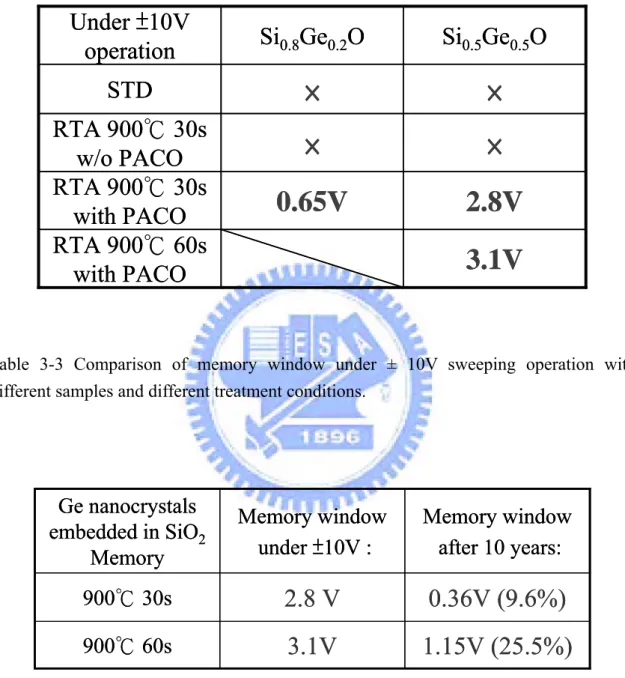
Table 3-3 Comparison of memory window under ± 10V sweeping operation with different samples and different treatment conditions.
Table 3-4 Comparison of memory window under ± 10V sweeping operation and remained charge ratio after 10 years with different thermal treatment time
Chapter 4
Table 4-1 Surface atomic concentration ratio of the sample III (Si0.5Ge0.5N) from
X-ray photoelectron spectroscopy (XPS) analysis.
Table 4-2 Comparison of memory window under ± 10V sweeping operation and remained charge ratio after 10 years with different thermal treatment conditions.
Table 4-3 Comparison of memory window under ± 10V sweeping operation with different samples and different treatment conditions.
Chapter 5
Table 5-1 Energy Dispersive X-ray Spectrometer (EDS) analysis of the control sample IV (ErSiGeO).
Table 5-2 Comparison of memory window under ± 10V sweeping operation with different samples and thermal treatment conditions (with PACO).
Figure Captions
Chapter 1
Figure 1-1 The structure of the conventional floating-gate (FG) nonvolatile memory device. Continuous poly-silicon gate is used as the charge storage element. Figure 1-2 The structure of the SONOS nonvolatile memory device. The nitride layer
is used as the charge storage element.
Figure 1-3 The development of gate stack of SONOS EEPROM memory devices. The optimization of nitride and oxide films has been main focus in recent years. Figure 1-4 The structure of the nanocrystal (NC) nonvolatile memory device. The
isolated nanocrystal with each other is used as the charge storage element.
Chapter 2
Figure 2-1 ID-VGS curves of the floating-gate NVM device, with before (curve A) and
after (curve B) negative charge Q is stored in the floating gate.
Figure 2-2 Energy band diagrams of the SONOS memory device under (a) program (b) erase operation. (e- : electrons, h+: holes.)
Figure 2-3 (a) The cross-section of nanocrystal memory device structure; (b) illustration of write process: inversion-layer electrons tunnel through tunnel oxide and inject into the nanocrystal; (c) illustration of erase process: accumulation layer holes tunnel through tunnel oxide and inject into the nanocrystal, electrons in nanocrystal also can tunnel back to the channel. Figure 2-4 Schematics of channel hot electron injection (CHEI). The energy
distribution function at point (X1,Y1) is also shown.
Figure 2-5 A schematic energy band diagram describing the different processes involved in electron injection.
Figure 2-6 Fourth approaches to programming methods (a) Direct tunneling (DT) (b) Fowler-Nordheim (FN) tunneling (c) Modified Fowler-Nordheim (MFN) tunneling (d) Trap assistant tunneling (TAT).
Figure 2-8 The procedure of band to band hot hole injection.
Figure 2-9 A typical result of an endurance test on a single cell. Threshold voltage window closure as a function of program / erase cycles.
Chapter 3
Figure 3-1 Schematics of the experimental process flow with co-sputtering silicon and germanium targets.
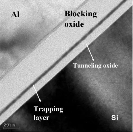
Figure 3-2 Cross-sectional TEM images of the MOIOS structure after a 900 60sec ℃ RTO process.
Figure 3-3 Ge 2p XPS analysis of the sample after 900 60sec RTO process. The peak ℃ position about 1220eV is the GeO2 signal.
Figure 3-4 Capacitance-voltage (C-V) hysteresis of the fabricated MOIOS structure after a 900 60sec RTO process.℃
Figure 3-5 The band diagram for the charge trapping center for GeO2 layer MOIOS
structure.
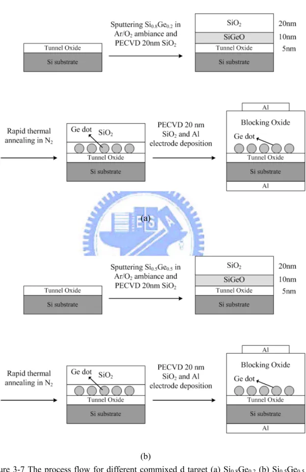
Figure 3-6 The process flow for different co-mixed target (a) Si0.8Ge0.2 (b) Si0.5Ge0.5
without pre-annealing capping oxide (PACO).
Figure 3-7 The process flow for different co-mixed target (a) Si0.8Ge0.2 (b) Si0.5Ge0.5
with pre-annealing capping oxide (PACO) step.
Figure 3-8 The XPS analysis by using an Al Kα (1486.6 eV) x-ray radiation is demonstrated the chemical composition of the sample I (Si0.8Ge0.2O) (a) Si
2p (b) Ge 3d (c) O 1s core-level spectra.
Figure 3-9 The XPS analysis by using an Al Kα (1486.6 eV) x-ray radiation is demonstrated the chemical composition of the sample II (Si0.5Ge0.5O) (a) Si
2p (b) Ge 3d (c) O 1s core-level spectra.
Figure 3-10 Cross-sectional TEM images of standard Sample II (Si0.5Ge0.5O) without
any thermal treatment.
Figure 3-11 Capacitance-voltage (C-V) hysteresis of (a) standard sample I (b) standard sample II.
Figure 3-12 Capacitance-voltage (C-V) hysteresis of (a) sample I Si0.8Ge0.2O (b) sample
II Si0.5Ge0.5O after RTA at 900 for 30sec without PACO.℃
Figure 3-13 Cross-sectional TEM images of the Sample II (Si0.5Ge0.5O) after RTA at
Figure 3-14 (a) SIMS depth profile of the standard sample II (Si0.5Ge0.5O).
Figure 3-14 (b) SIMS depth profile of the sample II (Si0.5Ge0.5O) after RTA at 900 for ℃
30sec without PACO. (c) comparison of the SIMS depth profile for the sample II with and without RTA treatment.
Figure 3-15 Capacitance-voltage (C-V) hysteresis of sample I Si0.8Ge0.2O after RTA at
900 for 30sec with PACO.℃
Figure 3-16 (a) and (b) TEM diagram of the sample I (Si0.8Ge0.2O) after RTA at 900 ℃
for 30sec with PACO.
Figure 3-17 SIMS depth profile of the sample II (Si0.5Ge0.5O) after RTA at 900 for ℃
30sec with PACO.
Figure 3-18 Capacitance-voltage (C-V) hysteresis of sample II Si0.5Ge0.5O after RTA at
900 for 30sec with PACO.℃
Figure 3-19 (a) and (b) TEM diagram of the sample II (Si0.5Ge0.5O) after RTA at 900 ℃
for 30sec with PACO.
Figure 3-20 Comparison of the SIMS depth profile for the sample II before and after RTA at 900 for 30sec℃ with PACO.
Figure 3-21 Different sample I and sample II after RTA 900 30sec with PACO (a) ℃ comparison of SIMIS depth profile (b) C-V curve of the sample II (c) C-V curve of the sample I.
Figure 3-22 Capacitance-voltage (C-V) hysteresis of sample II Si0.5Ge0.5O after RTA at
900 for 60sec with PACO.℃
Figure 3-23 (a) and (b) TEM diagram of the sample II (Si0.5Ge0.5O) after RTA at 900 ℃
for 60sec with PACO.
Figure 3-24 The X-ray photoelectron spectroscopy (XPS) analysis of the Ge 3d core-level spectrum. The Ge-O signal is at about 31eV shift to lower bonding energy 29 eV which is the Ge-Ge signal peak position before thermal treatment (RTA).
Figure 3-25 (a) Data retention characteristics of the Ge nanosrystals embedded in SiOx
memory with RTA at 900 for 30sec.℃
Figure 3-25 (b) Data retention characteristics of the Ge nanosrystals embedded in SiOx
memory with RTA at 900 for 60sec.℃
Figure 3-26 (a) The band diagram of the MOIOS structure as measuring current density-voltage (J-V) characteristics.
Figure 3-26 (b) The current density-voltage (J-V) of Ge nanocrystals embedded in SiOx
memory with and without thermal treatment (RTA).
Figure 3-27 Endurance characteristics of the Ge nanocrystal memory after RTA at (a) 900 for 30sec (b℃ ) 900 for 60sec.℃
Chapter 4
Figure 4-1 The process flow for sputtering Si0.5Ge0.5 co-mixed target in Ar/N2
ambiance with pre-annealing capping oxide (PACO) step
Figure 4-2 The XPS analysis by using an Al Kα (1486.6 eV) x-ray radiation is demonstrated the chemical composition of the sample III (Si0.5Ge0.5N) (a) Si
2p (b) Ge 3d (c) N 1s core-level spectra.
Figure 4-3 Cross-sectional TEM images of standard Sample III (Si0.5Ge0.5N) without
any thermal treatment.
Figure 4-4 Capacitance-voltage (C-V) hysteresis of standard sample III (Si0.5Ge0.5N)
without any thermal treatment.
Figure 4-5 Capacitance-voltage (C-V) hysteresis of sample III Si0.5Ge0.5N after RTA at
900℃ for 30sec with PACO.
Figure 4-6 TEM diagram of the sample III (Si0.5Ge0.5N) after RTA at 900℃ for 30sec
with PACO.
Figure 4-7 Capacitance-voltage (C-V) hysteresis of sample III Si0.5Ge0.5N after RTA at
900℃ for 60sec with PACO.
Figure 4-8 TEM diagram of the sample III (Si0.5Ge0.5N) after RTA at 900℃ for 60sec
with PACO.
Figure 4-9 (a) Data retention characteristics of the Ge nanocrystals embedded in SiNx
memory with RTA at 900 for ℃ 30sec.
Figure 4-9 (b) Data retention characteristics of the Ge nanocrystals embedded in SiNx
memory with RTA at 900 for ℃ 60sec.
Figure 4-10 Endurance characteristics of the Ge nanocrystal memory after RTA at (a) 900 for 30sec (b) 900 for 60sec.℃ ℃
Figure 4-11 The current density-voltage (J-V) of Ge nanocrystals embedded in SiNx
memory with different thermal treatment (RTA) time.
Figure 4-12 (a) and (b) The band diagram for Ge nanocrystals embedded in different dielectric memory. (a) in SiOx (b) in SiNx.
Chapter 5
Figure 5-1 The process flow for co-sputtering Si0.5Ge0.5 co-mixed target and Er target
in Ar/O2 ambiance with pre-annealing capping oxide (PACO) step.
Figure 5-2 Cross-sectional TEM images of standard Sample IV (ErSi0.5Ge0.5O) without
any thermal treatment.
Figure 5-3 Capacitance-voltage (C-V) hysteresis of standard sample IV (ErSi0.5Ge0.5N)
without any thermal treatment.
Figure 5-4 Cross-sectional TEM diagram of the sample IV (Si0.5Ge0.5N) after RTA at
900℃ for 30sec with PACO.
Figure 5-5 The XPS analysis of Er 4d core-level spectrum for sample IV before and after RTA. After the RTA process, the peak signal of Er-O bonding shift toward higher binding energy indicating Er-O might react with their nearby Si atoms.
Figure 5-6 Capacitance-voltage (C-V) hysteresis of sample IV after RTA at 900℃ for 30sec with PACO.
Chapter 1
Introduction
1.1 General Background of Nonvolatile Memory
In recent years, the portable electronic products have widely applied in our life. Such as cellular phone, digital camera, laptop, PDA, memory cards, MP3 audio player, USB flash personal disk etc. These products are all based on flash memory which is nonvolatile and they can keep stored information when the power supply switches off. Flash memory also has several advantages, such as the ability to be electrical programmed and fast simultaneous block electrical erase in a single-cell, smaller cell size to achieve higher chip density, and better flexibility [1.1-1.2]. The flash memory fabrication process can be compatible with the current CMOS process and be a suitable solution for embedded memory application. Flash memories are easily scale down and replacement for EPROMs (Erasable Programmable Read Only Memory) and EEPROMs (Electrically Erasable Programmable Read Only Memory). As these critical advantages flash memory possesses, it has become the mainstream nonvolatile memory device in last few decades.
In 1960’s, due to the high cost, large volume and high power consumption of the magnetic-core memory, the electronic industries urgently required a new kind of memory to replace the magnetic-core memory. In 1967, D. Kahng and S. M. Sze invented a new structure called floating-gate (FG) nonvolatile semiconductor memory at Bell Labs [1.3]. A standard conventional floating-gate device structure is shown in Figure 1-1. The structure is basic on a Metal Oxide Semiconductor Field Effect Transistor (MOSFET) with a modified stacking gate which composed by control gate, dielectric, floating gate and dielectric as a sandwich structure. Silicon dioxide (SiO2) is the most common
dielectric which the FG was embedded in. The FG acts as a charge storage node. Charges injected into the FG were retained there, resulting in the threshold voltage shift of the cell transistor for nonvolatile application.
Nowadays, nonvolatile memory device are moving toward higher density memory array, lower power consumption, low cost, higher speed operation and better reliability. Therefore the flash memory devices come to be in face of their limitations. Although the
conventional FG memory does not need refreshing, consume less power and achieve higher array density. However, the FG memory has slower operation speed and poor reliability. In order to improve the program / erase speed of the FG memory, the thickness of tunnel oxide must be reduced. The tunnel oxide must be thin enough to achieve fast and efficient charge transport ability. On the contrary, tunnel oxide needs to provide superior isolation under retention, endurance and disturbed conditions to keep the data integrity to 10 years. When the tunnel oxide becomes thinner, program speed will be faster. But if we need better isolation and reliability, we should increase the thickness of the tunnel oxide. So that is a trade-off between the operation speed and the reliability. Currently, the tunnel oxide of the commercial flash memory devices is about 8-11nm, Resulting in high programming voltage and slow programming speed [1.4].
For the conventional FG memory, if there are several defects in the tunnel oxide after programming or erasing operated steps, might induce a leakage path. That make all charge stored in the FG leak back to the channel. That is why the conventional FG memory always needs thicker tunnel oxide to get better retention. In order to overcome the scaling limitations of the conventional FG structure, there are two most mentioned candidates. One is the semiconductor/oxide/nitride/oxide/semiconductor (SONOS) [1.5-1.7] nonvolatile memory device. The other one is nanocrystal [1.8-1.10] nonvolatile memory device. These two structures have been demonstrated to improve the retention time compared to the conventional FG memory. Therefore, the tunnel oxide thickness could be decreased for faster operation speed and lower operation voltages.
1.2 SONOS Nonvolatile Memory Device
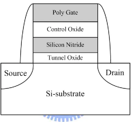
Poly silicon/control oxide/silicon nitride/tunnel oxide (SONOS) nonvolatile memory device structure is shown in Figure 1-2. The charge storage elements in SONOS memory are the charge traps distributed throughout the volume of the silicon nitride layer. It is well known that silicon nitride contain a lot of traps, and the trap density is about 1018-1019cm-3 according to Yang et al [1.11] and stores both electrons and holes (positive charges) injected from the channel. The first nitride-base devices is metal-gate nitride device MNOS (Metal/Nitride/Oxide/Silicon) which was reported in 1967 by Wegener et al [1.12]. Figure 1-3 illustrates the progression by the device cross section, which has led to the SONOS device structure. Initial device structures in the early 1970s were p-channel metal/nitride/oxide/silicon (MNOS) structure with aluminum gate electrodes and 45nm thick silicon nitride charge storage layers. Write/erase voltages were typically
25-30 V. In the late 1970s and early 1980s, scaling moved to n-channel SNOS devices with program / erase voltages of 14-18 V. In the late 1980s and early 1990s, n- and p-channel SONOS devices emerged with program / erase voltages of 5-12 V. In the SONOS device, an oxide layer is introduced between the gate and the silicon nitride region. Thus, it forms the ONO (SiO2/Si3N4/SiO2) gate dielectric stack (Fig. 1-2) instead
the nitride layer with just a metal or semiconductor gate. The purpose of top blocking oxide is to reduce the charge injection from the control gate into nitride layer, limiting the memory window of both MNOS and SNOS devices.
The SONOS memory devices have attracted a lot of attention due to theirs several advantage over the conventional FG flash memory devices. Include reducing process complexity, getting higher operation speed, lowering operation voltage, improving endurance and elimination of drain-induced turn-on [1.13-1.15]. The main difference between the conventional FG flash and SONOS memory is the charging method. Conventional FG structure charges carrier in the continuous conductive polysilicon. On the other hand, SONOS structure charge carrier in the physical discrete traps of the silicon nitride dielectric. The charge stored in the silicon nitride can not move easily, hence the SONOS can bear the defect in the tunnel oxide induced the leakage path. Therefore, the SONOS memory device has better endurance the conventional FG memory.
The SONOS memory device still has to face the challenge in the future for high density nonvolatile memory application, which require lower power (<5V), lower power consumption, faster operation speed, longer retention time and superior endurance characteristics. A lot of approaches have been proposed for improving the SONOS performance and reliability. Chen et al. demonstrated a Si3N4 bandgap engineering (BE)
control method for better endurance and retention. A nitride with varied relative Si/N ratio throughout the film has increased the charge-trapping efficiency significantly [1.16]. She et al. demonstrates that high-quality nitride is applied as the tunnel dielectric for a SONOS-type memory device. Compared to control devices with SiO2 tunnel dielectric,
faster programming speed and better retention time are achieved with low programming voltage [1.17]. Chen et al. studies a polycrystalline silicon thin-film transistor (poly-Si TFT) with oxide/nitride/oxide (ONO) stack gate dielectrics and multiple nanowire channels for the applications of both nonvolatile silicon-oxide-nitride-oxide-silicon (SONOS) memory and switch transistor [1.18]. The proposed NW SONOS-TFT exhibits
superior memory device characteristics with high program/erase efficiency and stable retention characteristics at high temperature. Such a SONOS-TFT is thereby highly promising for application in the future system-on-panel display applications.
In recent research, high-k dielectric materials were proposed to replace the silicon nitride film as trapping layer, such as HfAlO and Al2O3 [1.19]. HfAlO with 10% Al2O3
has very similar band offset to pure HfO2. The conduction band offset of HfAlO with
respect to Si is the smallest (1.63 eV), compared to 2 eV for Si3N4 and 2.8 eV for Al2O3.
Hence, at the same gate bias where modified F-N tunneling dominates, the electron tunneling distance from the Si substrate to the conduction band of the storage dielectric layer is shortest in HfAlO and longest in Al2O3 [1.20]. The over-erase phenomenon in the
SONOS memory structure is minimized by using hafnium oxide (SOHOS) to replace silicon nitride (SONOS) as the charge storage layer. Unlike SONOS devices, SOHOS structures show a reduced over-erase phenomenon and self-limiting charge storage behavior under both erase and program operation. These are attributed to the differences in band offset and the crystallinity of the charge storage layer [1.21].
1.3 Nanocrystal Nonvolatile Memory Device
Nanocrystal nonvolatile memories are one particular implementation of storing charge by dielectric surround nanodots, and were first introduced in the early 1990s by IBM researchers who proposed flash memory with a granular floating gate made from silicon nanocrystals [1.8]. The name nanocrystal referred to a crystalline structure with a nanoscale dimension. And its electric properties are more similar to an atom or molecule rather than the bulk crystal. Figure 1-4 shows the nanocrystal nonvolatile memory device structure. We can find out that the nanocrystals are separated with each other and embedded in the gate dielectric layer. In the nanocrystal nonvolatile memory device, the charges were charged in the isolated nanocrystals instead of the continuous FG polysilicon layer. Each nanodots will typically store only a handful of electrons; collectively the charges stored in these dots control the channel conductivity of the memory transistor.
Nanocrystal NVM devices have been attracted a lot of attentions recently due to the potential to overcome the limitations of traditional FG NVM. Using the nanocrystal to store charge offers several advantages. The main one is the potential to use thinner tunnel oxide without sacrificing nonvolatility. This is quite attractive issue since reducing the tunnel oxide thickness is a main factor to lowering operating voltages and/or increasing
operating speed. This claim of improved scalability results not only from the distributed nature of the charge storage, which makes the storage more robust and fault-tolerant, but also from the beneficial effect of Coulomb blockade [1.22]. And the lateral charge migration phenomenon will be suppressed by the mutually isolated nanocrystals with each other. Quantum confinement effects (bandgap widening; energy quantization) can be exploited in sufficiently small nanocrystal geometries (sub-3nm dot diameter) to further enhance the memory performance. There are other important advantages for nanocrystal NVM device. First, the fabrication of the nanocrystal memories is more simplified and lower process cost as compared to the conventional FG memories. Second, due to the absence of drain to FG coupling, nanocrystal memories suffer less drain induced barrier lowering (DIBL) and therefore have intrinsically better punch-through characteristics. This advantage is gained a higher drain bias during the read operation, thus improving memory access time [1.23]. It allows using shorter channel lengths and therefore smaller cell area. Third, nanocrystal memories are characterized by excellent immunity to stress induced leakage current (SILC) and oxide defects due to the distributed nature of the charge storage in the nanocrystal layer. The other is low capacitive coupling between the external control gate and the nanocrystal charge storage layer. This does not only result in lower operating voltages, thus offsetting the benefits of the thinner tunnel oxide, it also removes an important design parameter (the coupling ratio) typically used to optimize the performance and reliability tradeoff.
The fabrication of a nonvolatile memory cell requires a perfect control of four parameters: (1) the thickness of tunnel oxide, (2) the density of nanocrystals, (3) the size of nanocrystals, and (4) the thickness of control oxide. An important issue of the nanocrystals memory is the average dot size and the nanocrystal density. Larger dot size provide faster program / erase speed due to smaller quantum confinement and coulomb blockade effects and hence better carrier tunneling injection. But it also shows undesirable disadvantages with large size nanocrystal. Stress induced leakage during retention is one of them to make the device worse reliability. And as the nanocrystal size increase, the density of nanocrystal will be decrease. Thus it is also a trade-off between operating speed and reliability in selecting size of nanocrystal. A typical target is a density at least 1012cm-2, and requires nanocrystal size be about 5 nm and below. Moreover, good process control is needed with regards to such nanocrystal features as: planar nanocrystal layer; inter-crystal interaction (lateral isolation); and crystal doping (type and level). Finally, it is preferred that that the fabrication process is simple and that
it uses standard semiconductor equipment.
After S. Tiwari proposed silicon nanocrystal memory devices instead of FG memory. In order to improve the data retention by Coulomb blockade effect, double layer silicon nanocrystal memory has been invented [1.24]. It seems interesting to use Ge nanocrystals rather than Si nanocrystals because of its smaller band gap and higher dielectric constant. Indeed King and Hu have recently demonstrated the superior memory properties of Ge based nanocrystal memories over those based on Si [1.25]. As the size and size distribution of the nanocrystals have been considered, She et al. [1.26] made a conclusion on Ge nanocrystal memory device that size around 5 nm is preferred to achieve fast programming speed and longer retention time. And size should not be scale below 5 nm due to the quantum confinement effect will be very significant.
There are several nonocrystal fabrication processes which have been demonstrated. Numerous effort have focused on obtaining a high density of nanocrystals through a variety of techniques including aerosol technique, ion implantation, direct chemical vapor deposition (CVD), evaporation deposition such as sputter, dual E-gun, MBE and re-crystallization annealing of amorphous silicon (α-si). Kim et al. used conventional low pressure chemical vapor deposition (LPCVD) to fabricate silicon nonocrystals at 620 ℃ [1.27]. Direct CVD of silicon is preferred over ion implantation and re-crystallization annealing because it is difficult to control the required amount of silicon in the stack. Further, nucleation and growth by CVD provides simpler processing to control the size and the density of nanocrystals. Silicon nanocrystals with density between 1011 and 1012cm-2 have been deposited in various dielectrics such as SiO2 Si3N4 and Al2O3 by
using CVD process. A higher density about 5×1011cm-2 was obtained on nitride surface, and the density was more than three times larger that on oxide surface[1.28]. Fernandesa
et al. acquired the higher Si quantum dots density (~1012cm-2) by integrating on
SiO2/Al2O3 tunneling dielectrics [1.29]. To fabricate Ge nanocrystals, the oxidation of
mixed SiGe films has been proposed [1.25]. As the SiGe layer be oxidized, the Ge element will be segregated and Si will be oxidized into SiO2 [1.30-1.31]. Ostraat et al.
proposed an aerosol silicon nanocrystal nonvolatile memory device with large threshold voltage shift (>3V), sub-microsecond program times, millisecond erase times, excellent endurance (>105 program/erase cycles), and long term retention (>106 sec) [1.32].As for the tunnel dielectric for nanocrystal NVM devices, high-k tunnel dielectric were investigated [1.16] [1.28] [1.33]. Results show that due to its unique band asymmetry in
programming and retention mode. Using high-k dielectric on Si channel offers lower electron barrier height and larger dielectric thickness resulted in much higher IG, Write/Erase/
IG, Retention ratio than SiO2. Therefore, we get faster program / Erase speed and longer
retention.
In the future, the primary drivers behind nanocrystal memories are the potential to reduce the tunnel oxide thickness, resulting in lower operating voltages, and the simplicity of a single poly-silicon process. But there are still challenges for nanocrystal memories in the long road to commercialization. Nanocrystal memories have yet to deliver on most of their promises. In reality, part of the voltage gain is offset because of the poor control gate coupling. For fabrication processes, it is hard to control the uniformity of the nanocrystal size and their physical locations in the channel. It is not a surprise that nanocrystal memories exhibit large device-to-device variation. Moreover, it has yet to be demonstrated that both the nominal and the statistical retention behavior are sufficient to meet true non-volatility requirements. Although single-dot memories have been demonstrated [1.34-1.35], but a more fundamental understanding of the scaling limits of nanocrystal memories is necessary, concentrating especially on the aspect of controlling channel conductance when relying on only a few discrete charge centers [1.36]. Finally, in order for that to happen, their claimed benefits will need to be more unambiguously substantiated, and a more appealing bundle of memory features will have to be demonstrated.
1.4 Motivation
For nonvolatile semiconductor memories is to achieve low power, low voltage performance. For nonvolatile flash memories, two limitation had encountered at the present time are: (1) The limited potential for continued scaling of device structure, The scaling limitation stems from the extreme requirements put on tunnel oxide layer. In order to get balance between program / erase speed and retention time, it is a trade-off to get the optimal tunnel oxide thickness. (2) The quality and strength of tunnel oxide after plenty of program / erase cycles. Once a leaky path has been created in tunnel oxide, all the charge stored in the floating gate will be lost. Therefore, two kinds of new structure was suggested, SONOS and nanocrystal NVM devices, are proposed to overcome this oxide quality limit of the conventional FG structure.
These technologies replace the FG structure with a great number of charge-storage nodes in the dielectric or in the nanocrystal. Unlike the FG, the local leakage path will not
cause the entire loss of information for the nanocrystal NVM device. This effectively prevents the leakage of all the stored charges out of the floating gate.
In this thesis, a new idea of crystallize nanocrystal was be proposed. We chose sputter system which is lower cost than furnace system. To deposited a SiGeO film by sputtering SiGe co-mix target in Ar/O2 ambient to replace the FG in flash structure. This
is a new process to deposit a ternary SiGeO compound. We also chose rapid thermal annealing (RTA) to reduce thermal budget than furnace annealing to avoid Ge over oxidizing. After thermal treatment, Ge in the SiGeO film will be segregated to form Ge nanodots embedded in the SiOx dielectric. And it shows memory effect and reaches the
requirement of retention of 10 years and reliability for NVM application. Furthermore , we proposed a other new ternary SiGeN compound. Using the similar process to form Ge nanodots embedded in SiNx dielectric. And it also show memory effect and reaches the
requirement for NVM application.
1.5 Organization of This Thesis
This dissertation is divided into six chapters. The contents in each chapters are described briefly as follows:
In chapter 1, general background of nonvolatile memory, conventional flash memory,
SONOS nonvolatile memory and nanocrystal memory are introduced.
In chapter 2, basics of program and erase operation are introduced.
In chapter 3, the Ge nanocrystal embedded in SiOx NVM structure, experimental process
flow, results and discussions will be stated in this chapter.
In chapter 4, the Ge nanocrystal embedded in SiNx NVM structure, experimental process
flow, results and discussions will be stated in this chapter.
In chapter 5, the Ge doped in Erbium silicate high-k dielectric film, which is a SONOS
type NVM structure, experimental process flow, results and discussions will be stated in this chapter.
Figure 1-1 The structure of the conventional floating-gate (FG) nonvolatile memory device. Continuous poly-silicon gate is used as the charge storage element.
Figure 1-2 The structure of the SONOS nonvolatile memory device. The nitride layer is used as the charge storage element.
Figure 1-3 The development of gate stack of SONOS EEPROM memory devices. The optimization of nitride and oxide films has been main focus in recent years.
Figure 1-4 The structure of the nanocrystal (NC) nonvolatile memory device. The isolated nanocrystal with each other is used as the charge storage element.
Chapter 2
Nonvolatile Memory Basic Principles
2.1 Introduction
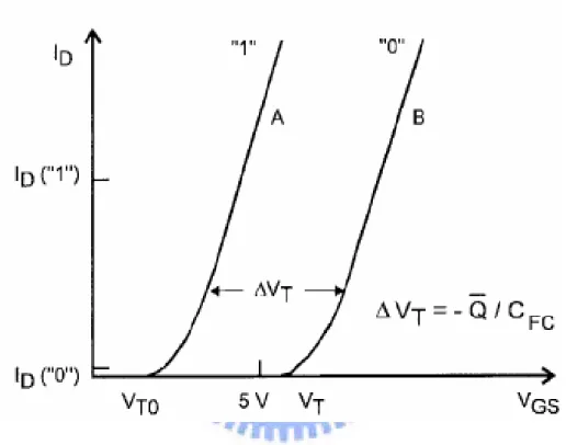
Most of operations on novel nonvolatile memories, such as SONOS and nanocrystal memories are base on the concept of Flash memory. If data was stored in selected cell of the memory, there are different procedures. The threshold voltage shift of a Flash transistor can be written as [2.1-2.2]:
FC T C Q V =− Δ
where Q is the charge weighted with respect to its position in the gate oxide, and the capacitances between the floating gate (FG) and control gate. The threshold voltage of the memory cell can be altered by changing the amount of charge present between the gate and the channel, corresponding to the two states of the memory cell, i.e., the binary values (“1” and “0”) of the stored bit. Figure 2-1 shows the threshold voltage shift between two states in a Flash memory. To a nonvolatile memory, it can be “written” into either state high state “1” or low state “0” by either “programming” or “erasing” methods, which are decided by the definition of memory cell itself. There are many solutions to achieve “programming” or “erasing”.
In this chapter, we will discuss program/erase mechanisms from the relation between bias and energy band bending. And different carrier injection mechanisms such as tunneling injection, channel hot electron injection and band to band tunneling. We will also discuss the reliability test briefly such as retention and endurance of NVM. Finally, some unique characteristic of nanocrystal memory will be discussed in the end of this chapter.
2.2 Basic Program/Erase Mechanisms
2.2.1 Energy band diagram during program and erase operation
The program/erase physical operation of a standard SONOS memory is illustrated in Figure 2-2. In the program operation, when a positive bias relative to the p-type substrate
applied on gate electrode, substrate induces an electron channel (inversion layer). Then the electron will tunnel through the tunnel oxide into the silicon nitride film and be trapped in deep level traps. Some electrons will not be trapped in the nitride film and will tunnel through the blocking oxide into gate electrode. The trapped electrons provide the electrostatic screening of the channel from the control gate, and result in a threshold voltage (VT) shift. In the erase operation, when a negative bias relative to the p-type
substrate applied on the gate electrode. The holes will tunnel through tunnel oxide into the nitride trapping layer and partially be trapped. Further, trapped electrons may be de-trapped into the nitride conduction band and then tunnel back to the channel. Thus, for SONOS memory device operation both carrier types are involved in the transport process.
Figure 2-3 illustrates schematically the write and erase operation of an n-channel nanocrystal memory. When the different bias applied on gate electrode, it causes different results. When the bias is positive relative to substrate, the electrons in the inversion layer inject in to the nanocrystal. That phenomenon is called “write operation”. On the contrary, negative bias applied to gate causes the electrons tunneling back to channel and the holes in the accumulation layer tunneling into the nanocrystal from the channel.
2.2.2 Carrier Injection Mechanisms
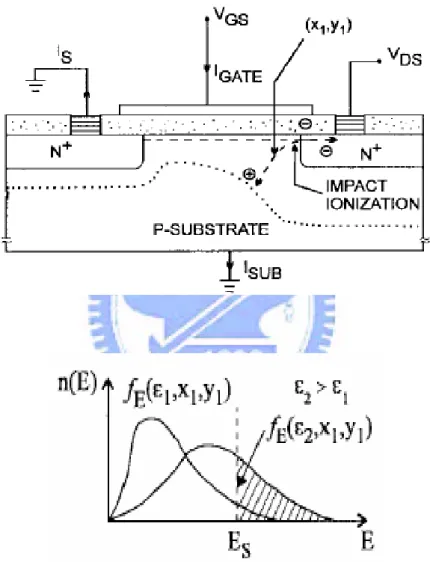
(a) Channel Hot Electron Injection (CHEI)
The physical mechanism of CHEI is relatively simple to understand qualitatively. An electron traveling from the source to the drain gains energy from the lateral electric field and loses energy to the lattice vibrations (acoustic and optical phonons). At low fields, this is a dynamic equilibrium condition, which holds until the field strength reaches approximately 105V/cm [2-3]. For fields exceeding this value, electrons are no
longer in equilibrium with the lattice, and their energy relative to the conduction band edge begins to increase. Electrons are “heated” by the high lateral electric field, and a small fraction of them have enough energy to surmount the barrier between oxide and silicon conduction band edges. Figure 2-4 shows schematic representation of CHEI MOSFET and the energy-distribution function with different fields.
In the other hand, the effective mass of hole is heavier than one of electron. It is too hard to obtain enough energy to surmount oxide barrier. Therefore, hot-hole injection rarely is employed in nonvolatile memory operation. For an electron to overcome this potential barrier, three conditions must hold [2.4].
(1) Its kinetic energy has to be higher than the potential barrier. (2) It must be directed toward the barrier.
(3) The field in the oxide should be collecting it.
Nevertheless, a description of the injection conditions can be accomplished with two different approaches. The CHEI current is often explained and simulated following the “lucky electron” model [2.5]. This model is based on the probability of an electron’s being lucky enough to travel ballistically in the field ε for a distance several times the mean free path without scattering, eventually acquiring enough energy to cross the potential barrier if a collision pushes it toward the Si/SiO2 interface. Consequently, the
probability of injection is the lumped probability of the following events [2.6], which are depicted in Figure 2-5.
(1) The carrier has to be “lucky” enough to acquire enough energy from the lateral electric field to overcome the oxide barrier and to retain its energy after the collision that redirects the electron toward the interface (PΦb).
(2) The carrier follows a collision-free path from the redirection point to the interface (PED).
(3) The carrier can surmount the repulsive oxide field at the injection point, due to the Schottky barrier lowering effect, without suffering an energy-robbing collision in the oxide (POC).
(b) Tunneling Injection
There are several tunneling mechanisms are demonstrated in quantum mechanics. Basically, tunneling injection must to have available states on the other side of the barrier for the carriers to tunnel into. The tunneling probability, depending on electron barrier height (φ(x) ), tunnel dielectric thickness (d), and effective mass (me) inside the tunnel
dielectric, is express as [2.7]
(2-1) If we assume elastic tunneling, this is a reasonable assumption due to the thin oxide thickness involved. Namely, no energy loss during tunneling processes. Tunneling through the oxide can be attributed to different carrier-injection mechanisms. Which process applies depends on the oxide thickness and the applied gate field or voltage.
Direct tunneling (DT), Fowler-Nordheim tunneling (FN), modified Fowler-Nordheim tunneling (MFN) and trap assistant tunneling (TAT) are the main programming mechanisms employed in memory [2.8-2.10] as shown in Figure 2-6.
Direct Tunneling
For nanocrystal memories, the control-gate coupling ratio of nanocrystal memory devices is inherently small [2.11]. As a result, F-N tunneling cannot serve as an efficient program/erase mechanism when a relatively thick tunnel oxide is used, because the strong electric field cannot be confined in one oxide layer. The direct tunneling is employed in nanocrystal memories instead. And that makes the nanocrystal memory with lower operation voltage and faster program/erase speed. Generally speaking, a thinner tunnel oxide with thickness below 5 nm is used to separate the nanocrystal from channel. In the other hand, the direct tunneling is more sensitive to the barrier width than barrier height, two to four orders of magnitude reduction in leakage current can still be achieved if large work function metals, such as Au or Pt [2.12]. Figure 2-6(a) shows the both sides barrier relative to thickness of the oxide that make electron direct tunneling through the oxide.
Fowler–Nordheim Tunneling
The Fowler–Nordheim (FN) tunneling mechanism occurs when applying a strong electric field (in the range of 8–10 MV/cm) across a thin oxide. In these conditions, the energy band diagram of the oxide region is very sharp. Hence, there is a high probability of electrons’ passing through the energy barrier itself. Using a free-electron gas model for the metal and the Wentzel–Kramers–Brillouin WKB approximation for the tunneling probability [2.13], one obtains the following expression for current density [2.14]:
⎥ ⎥ ⎦ ⎤ ⎢ ⎢ ⎣ ⎡− Φ Φ = ∗ qF m h F q J OX B B 3h ) 2 ( 4 exp 16 2 3 2 1 2 2 2 3 π (2-2) Where ФB is the barrier height, is the effective mass of the electron in the
forbidden gap of the dielectric, h is the Planck’s constant, q is the electronic charge, and F is the electric field through the oxide. However, the exponential dependence of tunnel current on the oxide-electric field causes some critical problems of process control because, for example, a very small variation of oxide thickness among the cells in a memory array produces a great difference in programming or erasing currents, thus
∗
OX
spreading the threshold voltage distribution in both logical states. Figure 2-6(b) shows the both sides barrier relative to thickness of the oxide that make electron Fowler–Nordheim tunneling through the oxide.
Modified Fowler–Nordheim Tunneling
Modified Fowler–Nordheim tunneling (MFN) is similar to the traditional FN tunneling mechanism, the carriers enter the nitride at a distance further from the tunnel oxide-nitride interface. MFN mechanism is frequently observed in SONOS memories. The SONOS memory is designed for low-voltage operation (<10 V, depending on the Equivalent oxide thickness), a relatively weak electrical field couldn’t inject charges by DT or FN mechanism. Figure 2-6(c) shows the both sides barrier relative to thickness of the oxide that make electron Modified Fowler–Nordheim (MFN) tunneling through the dielectric.
Trap Assistant Tunneling
The charge storage elements with many traps may cause another tunneling mechanism. For instance, the charges tunnel through a thin oxide and arrive to the traps of nitride layer at very low electrical field in SONOS systems. During trap assisted injection the traps are emptied with a smaller time constant then they are filled. The charge carriers are thus injected at the same distance into the nitride as for MFN injection. Because of the sufficient injection current, trap assistant tunneling may influence in retention [2.15]. Figure 2-6(d) illustrates the Trap Assistant Tunneling through the dielectric.
(c) Band to Band Tunneling (BTBT)
Band to band tunneling application to nonvolatile memory was first proposed in 1989. I. C. Chen and et al. demonstrated a high injection efficiency (~1%) method to programming EPROM devices [2.16]. Band to band tunneling (BTBT) process occurs in the deeply depleted doped surface region under the gate to drain or gate to source overlap region.
Band to Band Hot Electron Tunneling Injection
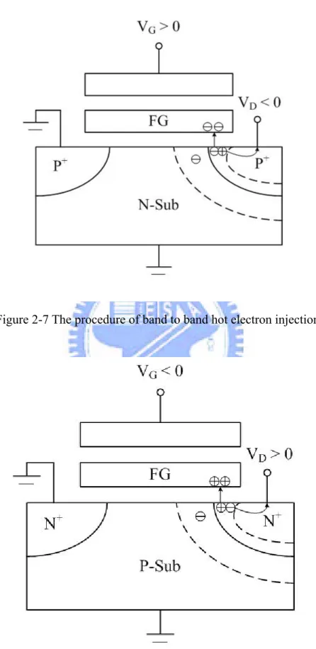
In n-type substrate, when band-bending is higher than the energy gap of the semiconductor, the tunneling electron from the valence band to the conduction band becomes significant. The electrons are accelerated by a lateral electric field toward the
channel region and some of the electrons with sufficient energy can surmount the potential barrier of SiO2 like hot electron injection [2.16-2.18]. Figure 2-7 shows device
operation during the band to band tunneling induced hot electron (BBHE) injection.
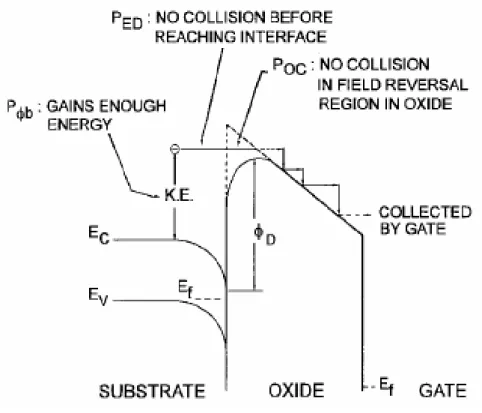
Band to Band Hot Hole Tunneling Injection
The injection is applied for p-type nonvolatile memory device. The mechanism is at the situation for both negative gate voltage and positive drain voltage. Electron-hole pairs are generated by BTBT in the drain region, as shown in Figure 2-8. The holes are accelerated by a lateral electric field toward the channel region and some of them obtain high energy. The hot holes with high energy will inject into charge trapping layer through the tunnel oxide and recombine with the stored electrons. This injection is used for a new erase operation for nonvolatile memory device [2.19].
2.3 Basic Reliability of Nonvolatile Memory
For a nonvolatile memory, the important to concern is distinguishing the state in cell. However, in many times operation and charges storage for a long term, the state is not obvious with charges loss. Retention and endurance experiments are performed to investigate Flash-cell reliability. In general, NVMs are required to achieve up to 10-100K program/erase cycles (endurance) with 10-year memory retention at temperatures as high as 85 °C.
2.3.1 Retention
Retention means that how long does the memory keep the information without losing it. In any nonvolatile memory technology, it is essential to retain data for over ten years. This means the loss of charge stored in the storage medium must be as minimal as possible. For example, in modern Flash cells, FG capacitance is approximately 1 fF. A loss of only 1 fC can cause a 1V threshold voltage shift. If we consider the constraints on data retention in ten years, this means that a loss of less than five electrons per day can be tolerated [2.1]. There are four possible causes of charge loss: 1) by tunneling or thermionic emission mechanisms; 2) defects in the tunnel oxide; and 3) de-trapping of charge from insulating layers surrounding the storage medium; 4) mobile ion contamination. Further, the retention capability of Flash memories has to be checked by using accelerated tests that usually adopt screening electric fields and hostile environments at high temperature.
2.3.2 Endurance
Endurance referred the number of erase/write operations that the memory will complete and continue to operate as specified in the data sheet. Generally speaking, Flash products are specified for 106 erase/program cycles. Nevertheless, the endurance requirement may be relaxed with the increase of memory density for the other using.
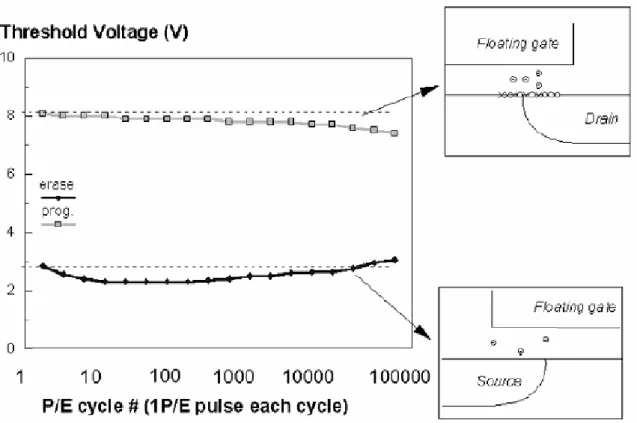
A typical result of an endurance test on a single cell is shown in Figure 2-9. As the experiment was performed applying constant pulses, the variations of program and erase threshold voltage levels are described as “program/erase threshold voltage window closure” and give a measure of the tunnel oxide aging [2.20-2.21]. In particular, the reduction of the programmed threshold with cycling is due to trap generation in the oxide and interface state generation at the drain side of the channel. The evolution of the erase threshold voltage reflects the dynamics of net fixed charge in the tunnel oxide as a function of the injected charge. The initial lowering of the erase is due to a pile-up of positive charge which enhances tunneling efficiency, while the long-term increase of the erase is due to a generation of negative traps.
Moreover, a high field stress on thin oxide is known to increase the current density at low electric field. The excess current component, which causes a significant deviation from the current–voltage curves from the theoretical F-N characteristics at low field, is known as stress-induced leakage current (SILC). SILC is clearly attributed by stress-induced oxide defects, which leads to a trap assisted tunneling. The main parameters controlling SILC are the stress field, the amount of charge injected during the stress, and the oxide thickness. For fixed stress conditions, the leakage current increases strongly with decreasing oxide thickness [2.22-2.24].
2.4 Basic Physical Characteristics of Nanocrystal Memory
2.4.1 Quantum Confinement Effect
The quantum dot, is quasi-zero-dimensional nanoscaled material, and is composed by small amount atoms. The quantum confinement energy dependence on nanocrystal size has been studied both experimentally and theoretically with the tight-binding model [2.25]. The quantum confinement effect becomes significant when the nanocrystal size shrinks to the nanometer range, which causes the conduction band in the nanocrystal to shift to higher energy compared with bulk material [2.26]. For instance, a 3nm Ge nanocrystal can have a conduction band shift up 0.5eV as compared with bulk Ge, which
is significant enough to affect the electrical performance of the nanocrystal memory cell.
2.4.2 Coulomb Blockade Effect
With a electron is stored, the nanocrystal potential energy is raised by the electrostatic charging energy e2
/2C, where C is the nanocrystal capacitance, which
depends mainly on the nanocrystal size, though it also depends on tunnel oxide thickness and control oxide thickness. The capacitance is self-consistently calculated using an electrodynamics method [2.27]. Charging electrons will raise the nanocrystal potential energy and reduce the electric field across the tunnel oxide, resulting in reduction of the tunneling current density during the write process. It is more dominant at low programming voltages (< 3V). In a flash memory array, device cells often encounter disturbances with low gate voltage soft-programming. The Coulomb blockade effect can effectively inhibit the electron tunneling at low gate voltage and improve the flash memory array immunity to disturbance. However, the Coulomb blockade effect should be reduced by employing large nanocrystal if large tunneling current and fast programming speed were considered. The Coulomb blockade effect has a detrimental effect on the retention time, since the electrons in the nanocrystal have large tendency to tunnel back into the channel if the nanocrystal potential energy is high in retention mode.
Figure 2-1 ID-VGS curves of the floating-gate NVM device, with before (curve A) and
Figure 2-2 Energy band diagrams of the SONOS memory device under (a) program (b) erase operation. (e- : electrons, h+: holes.)
Figure 2-3 (a) The cross-section of nanocrystal memory device structure; (b) illustration of write process: inversion-layer electrons tunnel through tunnel oxide and inject into the nanocrystal; (c) illustration of erase process: accumulation layer holes tunnel through tunnel oxide and inject into the nanocrystal, electrons in nanocrystal also can tunnel back to the channel.
Figure 2-4 Schematics of channel hot electron injection (CHEI). The energy distribution function at point (X1,Y1) is also shown.
Figure 2-5 A schematic energy band diagram describing the different processes involved in electron injection.
(a) (b)
DT occur when OT OT OT X E X 2 1 1 φ φ −φ FN occur when OT OT X E > φ1 > >(c) (d)
MFN occur when TAT occur when
N N OX OT OT OT X X E X ⎟ ⎠ ⎞ ⎜ ⎝ ⎛ + − > > − ε ε φ φ φ φ1 2 1 2
N N OX OT OT OT X X E X ⎟ ⎠ ⎞ ⎜ ⎝ ⎛ + > > ε ε φ φ3 3 t φ φ φ φ3 = 1− 2 −
Figure 2-6 Fourth approaches to programming methods (a) Direct tunneling (DT) (b) Fowler-Nordheim (FN) tunneling (c) Modified Fowler-Nordheim (MFN) tunneling (d) Trap assistant tunneling (TAT).
Figure 2-7 The procedure of band to band hot electron injection.
Figure 2-9 A typical result of an endurance test on a single cell. Threshold voltage window closure as a function of program / erase cycles.
Chapter 3
Formation of Germanium Nanocrystals
Embedded in Silicon Oxide Layer
3.1 Introduction
The nonvolatile memory (NVM) for portable electronic productions play an important role in semiconductor industrial because of its superiority in low-power consumption, low-cost, high-memory capacity and enough data retention[3.1][3.2]. The conventional NVM, however, can’t efficaciously prevent data loss in terms of reliability trials for future scaling down process, since its charge trapping layer is fabricated by floating gate (FG) structure and its tunnel oxide is ultra thin film about 2-5 nm[3.3][3.4]. Due to the discrete charge storage nodes acting as charge trapping layer to reform drawbacks of conventional FG memory, the NVMs using various semiconductor nanocrystals have been widely investigated in the past few years , such as silicon (Si) , germanium (Ge) and Zine-Oxide (ZnO) nanocrystals[3.2][3.5]. Moreover, in order to improve operation speed one can replace silicon nanocrystals (NC-Si) by germanium nanocrystals (NC-Ge) thanks to its higher dielectric constant (~16.0, i.e., stronger coupling with the conduction channel). In the other way, Ge nanocrystals device will improve data retention time due to its smaller energy band gap. Indeed King et al. [3.6] have reported recently superior properties for NC-Ge base on memory over than NC-Si in terms of writing/erasing time.
According to the current research, the self-assembled and direct growth of Ge nanocrystals embedded in SiO2 layer has successfully been implemented such as Ge
implantation into SiO2 [3.7-3.8], oxidation reduction of Ge/Si islands [3.9], UV-assisted
oxidation of Si1-xGex alloy [3.10], and rapid thermal oxidation (RTO) of NC-Ge
[3.11-3.12] or Ge + SiO2 [3.13]. Among various formation methods, the self-assembled
was reported by many previous studies because it could control better density and size of nanocrystal than direct growth. Nevertheless, the self-assembled method must need a high temperature (~900-1100℃) with long duration (~30-60 min) oxidation process to
anneal the charge trapping layer that is deposited by various ratio of SiGe layer, and the over-oxidation phenomenon of Ge is often obtained after foregoing oxidation process. Hence, an additional step must be added to the formation flow of Ge nanocrystal by using a high pressure H2 treatment [3.14-3.15] or steam process [3.16].
In order to reduce process flow and thermal budget, we choose the sputter system and rapid thermal anneal (RTA) for our experiments.
3.2 Growth SiGe and oxidation
There were a lot of experiments forming Ge nanocrystal by oxidizing the SiGe film. The SiGe film might be deposited by different process such as low pressure chemical vapor deposition (LPCVD), sputter system, plasma enhanced chemical vapor deposition (PECVD). At the same, we tried to deposit SiGe thin film by co-sputter and thermal treatment.
3.2.1 Experimental Sample Preparation
Figure 3-1 shows schematics of the experimental process flow. This nonvolatile memory-cell structure in this study was fabricated on a 4 inches p-type silicon (100) wafer, which had been removed native oxide and particles by RCA process. After a standard RCA clean, a 3-nm-thick tunnel oxide was thermally grown by a dry oxidation process at 950 in an atmospheric pressure chemical vapor deposition (APCVD) ℃ furnace. Subsequently, a 7-nm-thick SiGe film was deposited on tunnel oxide by co-sputtering Si and Ge targets in Argon (Ar) ambiance at room temperature, and the Ar flow rate was set to 24 sccm (Standard Cubic Centimeter per Minute). And then we deposited a 10-nm-thick pure amorphous Si by sputtering Si target in pure Ar ambiance. And the we oxidized the sample by rapid thermal anneal (RTA) at 900℃ 60sec in Oxygen ambiance. Expected Germanium nanocrystal could be found to precipitate and embed in silicon oxide. During the rapid thermal oxidation (RTO) process, the Si layer capped on the SiGe film was formed blocking oxide at the same time. Al gate electrodes on back and front side of the sample were finally deposited and patterned to form a metal/oxide/insulator/oxide/silicon (MOIOS) structure.
Electrical characteristics of the capacitance-voltage (C-V) hysteresis were measured by Keithley 4200 and HP4284 Precision LCR Meter with high frequency 1 MHz. In addition, transmission electron microscope (TEM) and X-ray photoelectron spectroscopy (XPS) were adopted for the micro-structure analysis and chemical material analysis.
3.2.2 Results and Discussion
Figure 3-2 shows the TEM of the sample after RTO process. We can find out the charge trapping layer became a continuous film. The XPS analysis by using an Al Kα (1486.6 eV) x-ray radiation is demonstrated the chemical composition of the charge trapping layer, as shown in figure 3-3. From the Ge 2p core-level spectrum, we can see that the GeO2 peak is at about 1220 eV by fitting results. Therefore, we think the entire
trapping layer was over-oxidized and the Ge layer all became GeO2. The
capacitance-voltage (C-V) hysteresis is shown in figure 3-4. It is clearly observed that 0.5V memory window was obtained under ± 5 V gate voltage operation. And the hysteresis loops follow the counterclockwise due to injection of electrons from the deep inversion layer and discharge of electrons from the deep accumulation layer of Silicon substrate. Hence, we can be enough to define “1” and “0” states for nonvolatile memory application. Figure 3-5 shows the band diagram of our sample after RTO 900 60sec. ℃ GeO2 energy band gap is about 4 eV [3.17]. Due to GeO2 providing some charge traps
and the interface trap with tunnel oxide, this sample still has memory effect.
According to the previous experiment result, we can find out some results: (1) the co-sputter method is hard to control the Si/Ge ratio; (2) conventional oxidation of SiGe layer is hard to control the oxidation time; (3) as our sample, the Ge was all oxidized and became GeO2 likes the below formula.
SiGe + O2 → SiO2 + GeO2 (3-1)
There are some drawbacks from the above results, in ordering to solve the over oxidation problem. We propose a SiGeO film on tunnel oxide to avoid over-oxidation phenomenon.
3.3 Formation of Ge nanocrystal using SiGeO layer
3.3.1 Experimental Sample Preparation
This nonvolatile memory-cell structure in this study was fabricated on a 4 inches p-type silicon (100) wafer, which had been removed native oxide and particles by RCA process. After a standard RCA clean, a 5-nm-thick tunnel oxide was thermally grown by a dry oxidation process at 950℃ in an atmospheric pressure chemical vapor deposition (APCVD) furnace. Subsequently, a 8-nm-thick oxygen incorporated SixGe1-x (SiGeO)
layer was deposited on tunnel oxide by reactive sputtering of SixGe1-x commixed target in