國 立 交 通 大 學
電子工程學系 電子研究所
碩 士 論 文
非對稱輕摻雜汲極金屬氧化半導體電晶體
非對稱輕摻雜汲極金屬氧化半導體電晶體
非對稱輕摻雜汲極金屬氧化半導體電晶體
非對稱輕摻雜汲極金屬氧化半導體電晶體
應用於
應用於
應用於
應用於2.4GHz
2.4GHz
2.4GHz
2.4GHz 射頻功率放大器
射頻功率放大器
射頻功率放大器
射頻功率放大器
A 2.4GHz RF CMOS Power Amplifier
Using High Breakdown Voltage
Asymmetric-LDD MOS Transistors
研究生: 陳膺任
指導教授: 荊鳳德 博士
I
非對稱輕摻雜汲極金屬氧化半導體電晶體
非對稱輕摻雜汲極金屬氧化半導體電晶體
非對稱輕摻雜汲極金屬氧化半導體電晶體
非對稱輕摻雜汲極金屬氧化半導體電晶體
應用於
應用於
應用於
應用於2.4GHz
2.4GHz
2.4GHz
2.4GHz 射頻功率放大器
射頻功率放大器
射頻功率放大器
射頻功率放大器
學生
學生
學生
學生:
: 陳膺任
:
:
陳膺任
陳膺任
陳膺任
指導教
指導教
指導教
指導教授
授:
授
授
:
: 荊鳳德
:
荊鳳德
荊鳳德
荊鳳德
博士
博士
博士
博士
國立交通大學電子工程學系電子研究所
國立交通大學電子工程學系電子研究所
國立交通大學電子工程學系電子研究所
國立交通大學電子工程學系電子研究所
摘要
摘要
摘要
摘要
本論文展示了一種以非對稱輕摻雜汲極金氧半體電晶體作為功率單元的 2.4GHz 射頻功率放大器架構,該放大器可完全以 TSMC 0.18um 的 CMOS 一般製程環境來 實現。這個設計可以穩定的操作在 2.5V ~ 2.75V,而不需使用串接電路。較高 的操作電壓使得電路有優越的功率特性,根據晶片實際量測的結果,2.5V 工作 電壓條件下,功率增益達 20dB,功率增加效率(PAE)達 30%,2.75V 的工作電壓 條件下,輸出功率 P1dB 可達 21.5dBm 飽和輸出功率可達 23.2dBm,並且測得 W-CDMA π/4 QPSK調變下,鄰近通道功率比在 15dBm 的輸出功率為-41dBc,與大 約 36dBm 的輸出三階互調截點(OIP3)。 關鍵字 關鍵字 關鍵字 關鍵字::::金氧半導體電晶體功率放大器,非對稱金氧半導體電晶體,功率單元, 崩潰電壓,功率增加效率,功率增益,1dB 的功率壓縮點,單晶片系統
II
A 2.4GHz RF CMOS Power Amplifier Using
High Breakdown Voltage Asymmetric-LDD
MOS Transistors
student: Ying Jen Chen
Advisor: Dr. Albert Chin
Department of Electronics Engineering and Institute of Electronics
National Chiao Tung Universityu, Hsinchu, Taiwan, R.O.C.
Abstract
This thesis presents a 2.4 GHz RF CMOS power amplifier based on two stages amplifiers topology with asymmetric-lightly-doped-drain (LDD) CMOS power cell which is fully embedded in the conventional foundry logic process with only one additional mask but without extra process step. The power amplifier can achieved higher output power and higher power-added efficiency (PAE) and novel linearity. The simulation result demonstrated 20dB power gain, and 30% PAE with 2.5V supply voltage, 21.5dBm at 1-dB compression point (P1dB), 23.2dBm saturate output power, -41dBc ACPR at 15dBm output power point with standard W-CDMA π/4 QPSK modulation , and ~36dBm OIP3 with 2.75V supply voltage.
Keywords: CMOS power amplifier, asymmetry –LDD CMOS, power cell,
III
誌 謝
首先感謝我的指導老師荊鳳德教授,老師熱誠的態度與對研究的敏銳度感激勵了 整個團隊,帶領我們,使研究不斷向前,精益求精。 在老師的指導下順利完成學業,讓我學習,成長了許多。在此致上我最深的尊敬 與感謝。 感謝我的家人,給我鼓勵及動力,是你們讓我能有美好的環境,有機會挑戰自我, 實現理想。 感謝交通大學ED633實驗室的全體同學,感謝張慈,高瑄苓博士,翁正彥學長在 生活上的照顧與研究上的指導。 特別感謝張慈學長給予我的建議與關心,提供我許多寶貴的經驗與機會參與中山 科學研究院的各項量測工作。 感謝同屆的同學熊旭廷,李富國,劉思麟,陳冠霖,黃俊哲,陳維邦,周坤億, 廖柏凱,周佑亮,凃宮強以及每一位一同修課的同學在學業上互相砥礪扶持,在 這兩年的研究生涯中一起經歷了美好的日子。感謝實驗室的學弟們,陳順芳,陳 冠翰,辜柏翔,陳鉅宗以及族繁不及輩載的學弟們,為碩士生活注入新鮮的活力。 感謝我在大學時時期的朋友,你們貼心關懷與支持讓我的腳步更堅定。 最後感謝國家晶片系統設計中心,提供實現晶片與量測晶片的環境。IV
Contents
Abstract (in Chinese) ...……….………..………I
Abstract (in English) .…………..………..……….………....II
Acknowledgement .………..….………III
Contents ..……….……….……..………...IV
Table Captions ………...V
Figure Captions ………..………...VI
Chapter1
INTRODUCTION ………..1
1.1 introduction ………..1
1.2 challenge of CMOS power amplifier ………2
1.3 general statements of CMOS power amplifier
(literature Review) ……….………..……….…...4
1.4 motivation ………7
Chapter2
DESIGN FLOW ……….………….…………8
2.1 Circuit design ……….………..8
2.2 Pre-layout simulation process ………..……….10
2.3 Post-layout simulation ……….….…………..18
Chapter3
SIMULATION AND MEASUREMENT RESULT ……..….……..21
3.1 simulation and measurement result ……….….……..21
Chapter4
COMPARISON
……….……….……...……..25
4.1 comparison ……….……...……..25
Chapter5
CONCLUTION ……….27
5.1conclution ……….27
V
TABLE CAPTIONS
Chapter 1
P.1
Table 1.1
implementation of system with different application 2Table 1.2
comparison table of different power cell 5Chapter 2
P.8
Table 2.1
design goal 11Chapter 4
P.25
VI
FIGURE CAPTIONS
Chapter 1
P.1
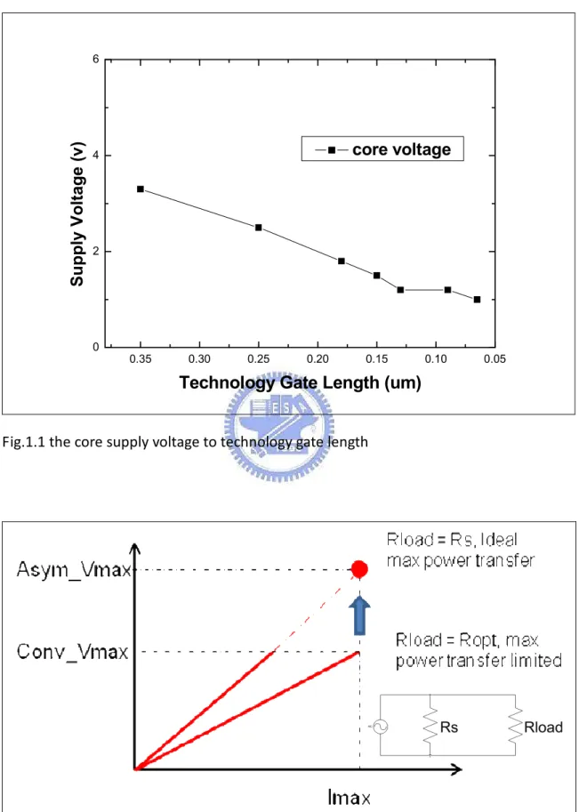
Fig. 1.1 the core supply voltage to technology gate length 3
Fig. 1.2 V-I load line show that If increase breakdown voltage, the output power
can approach ideal maximum power transfer with Rload = Rs. 3
Fig. 1.3 (a)Device structure of asymmetric-LDD MOS transistor . 4
(b)breakdown voltage of asymmetric –LDD mosfet and conventional mosfet
Chapter 2
P.8
Fig. 2.1 schematic of the two stage amplifier circuit 9
Fig. 2.2 Id-Vd analysis or the a-LDD MOSFET 10
Fig. 2.3 Id-Vd analysis and simulation with load line, gate voltage 12
Fig. 2.4 Id-Vd analysis and simulation with class AB operation 12
Fig. 2.5 simulation of the transistor loading currents with class AB operation 13
Fig. 2.6 ideal lump schematic 13
Fig. 2.7 tsmc model schematic 14
Fig. 2.8 Input matching 15
Fig.2.9 output load pull trade off 15
Fig.2.10 stability factor > 1 16
VII
Fig. 2.12 the layout before post layout simulation 17
Fig. 2.13 Export the line of layout to momentum ADS system and simulation 18
Fig. 2.14 Layout simulation with line calculation 19
Fig. 2.15 the layout after post layout simulation 20
Fig. 2.16 the photograph of the chip 20
Chapter 3
P.21
Fig. 3.1 Measured and simulated gain and return loss for CMOS PA 21
Fig. 3.2 Measured and simulated RF output power, gain and PAE of designed PA
using high breakdown voltage asymmetric-LDD MOSFETs 23
Fig. 3.3 Measured ACPR of designed PA using high breakdown voltage
asymmetric-LDD MOSFETs 23
Fig. 3.4 measurement data of IP3 with 1.8V supply voltage 24
Fig. 3.5 measurement data of IP3 with 2.5V supply voltage 24
- 1 -
Chapter 1
INTRODUCTION
In RF circuit design, Power Amplifiers are the most power-hungry building blocks of
RF transceivers. Large supply voltage is requirement for practical application. CMOS
PA design will face the great impact and hard to survive in advance technology
implementation with low supply voltage in the future.
The CMOS process reduce the minimum channel length in recent years, unit current
gain cut off frequency (ft) has increased, For instance, Tsmc 0.13um technology, ft is
above 100GHz and maximum oscillation frequency (fmax) is about 80GHz [1]; for
Tsmc 0.18um technology, ft is about 51 GHz, fmax is about 76GHz. These results are
suitable for present protocol. CMOS technology has made great progress, it almost
has implemented all blocks in system successfully, such as baseband processor,
microprocessor, flash memory, VCO, LNA, mixer [Table 1.1]. CMOS technology
became the most common back-end system implementation. The approach of
system on a chip (SOC) can avoid expensive and individual bulky hardware or
complexity system in package (SIP) technique.
However, designers suffered from realizing the direct conversion RF system for
several years, especially power amplifier building block. Because something cost
- 2 -
1.2 Challenge of CMOS power amplifier
Fig. 1 show the supply voltage of advance technology that decreases when gate
length decrease. The practical supply voltage of power amplifier is 3.3V but the
logic-core supply voltage even less than 1.2V after 90nm technology. Therefore, low
output power standard like Bluetooth, 0~4dBm can be realized, but large output
power would be limited by CMOS characteristic. A fatal drawback of CMOS is low
breakdown voltage. The problem limited the supply voltage that limits the maximum
output power of power amplifier [Fig. 1.2]. The optimum output loading design
becomes a complex and critical issue in power amplifier design. Therefore, CMOS
power amplifier has been one of the most challenging circuits and still defied an
elegant solution.
Table 1.1. implementation of system with different application
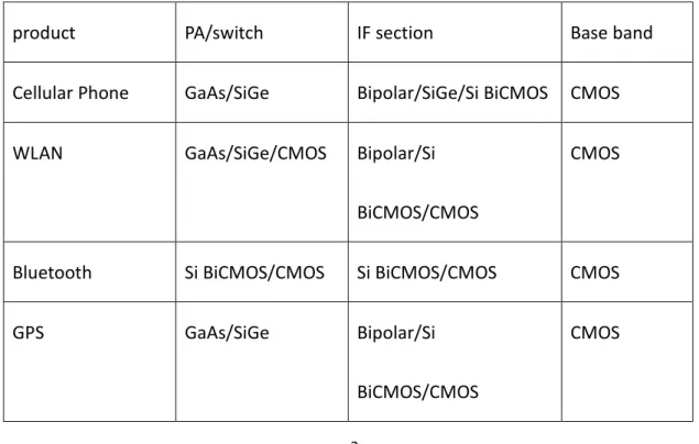
product PA/switch IF section Base band
Cellular Phone GaAs/SiGe Bipolar/SiGe/Si BiCMOS CMOS
WLAN GaAs/SiGe/CMOS Bipolar/Si
BiCMOS/CMOS
CMOS
Bluetooth Si BiCMOS/CMOS Si BiCMOS/CMOS CMOS
GPS GaAs/SiGe Bipolar/Si
BiCMOS/CMOS
- 3 - 0.35 0.30 0.25 0.20 0.15 0.10 0.05 0 2 4 6 S u p p ly V o lt a g e ( v )
Technology Gate Length (um)
core voltage
Fig.1.1 the core supply voltage to technology gate length
Fig. 1.2 V-I load line show that If increase breakdown voltage, the output power can approach ideal maximum power transfer with Rload = Rs.
- 4 -
1.3 General statement of CMOS power amplifier
What is the development of the present CMOS power amplifier? In fact, industry had
use CMOS power amplifier for lower output power application, such as bluetooth
and WLAN, the standard bluetooth is about 0 to 4dBm [2] and WLAN is about 15dBm.
But output power is still a limitation and it is rare larger output power application
designed by CMOS, the large output power application such as PHS 3G cell phone are
almost implemented by GaAs or SiGe. The limitation not only output power but also
efficiency, gain etc. If we want to make a break though the bottleneck, high
performance power cell would be the solution.
Resent years, our research group presents a new asymmetric-lightly-doped-drain
(LDD) MOS transistor [4], [5] that is fully embedded in a CMOS logic without any
process modification, so it can be easy implemented without any additional process
step or extra cost.
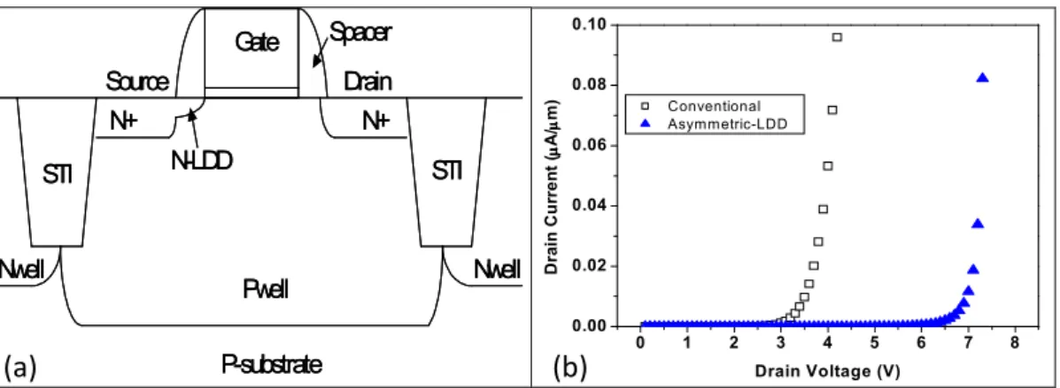
STI STI Gate N+ N+ Spacer N-LDD Pwell Nwell Nwell P-substrate Drain Source STI STI Gate N+ N+ Spacer N-LDD Pwell Nwell Nwell P-substrate Drain Source 0 1 2 3 4 5 6 7 8 0.00 0.02 0.04 0.06 0.08 0.10 D ra in C u rr e n t (µµµµ A /µµµµ m ) Drain Voltage (V) Conventional Asymmetric-LDD
Fig. 1.3 (a)Device structure of asymmetric-LDD MOS transistor .(b)breakdown
voltage of asymmetric –LDD mosfet and conventional mosfet
- 5 -
The major difference to conventional MOS transistor is no n+-LDD region at drain side. [Fig. 1.3(a)] The formed depletion region under reverse drain bias can sustain
large voltage for RF power application. Based on the research, this new structure can
overcome the low breakdown voltage issue and improve the RF power performance
[3], the breakdown can be 7.0V [Fig.1.3(b)] with still high unity current gain cut-off
frequency (ft). Focus on full embedded CMOS power cell, we compare three general
power cells to asymmetric LDD mos power cell with model simulation, those are
nmos unit cell, cascode cell, inverter CMOS push pull power cell. [Table. 1.2]
Table. 1.2 comparison table of different power cell
Tsmc_unit Asys_unit (our cell) Tsmc_Cascode (unit area) Tsmc_cascode (large area) Push pull Area (5x20) 1 1 1 2 1 Ft (GHz) 51 43 35 35 39 Fmax(GHz) 76 100 80 70 59 P1dB(dBm) 13.6 18.34 12.7 18.2 13.3 PAE @P1dB (%) 27.3 39.5 13.4 25.5 35.4
- 6 -
In addition, here shows a data of double area cascode (Two unit area - 6 - cascode)
to compare. It shows the asymmetric LDD nmos power cell has larger fmax, output
power (even larger than double area cascode output power) and efficiency than
others, and it indicates that the asymmetric LDD nmos has constitutional superiority
to construct power amplifier.
As technology evolution, the RF gain, cut-off frequency and noise figure of Si MOSFET
improve continuously that are widely used for wireless communications. However,
the RF power performance of Si MOSFET has little improvement with down-scaling,
which is limited by the inherent low breakdown voltage.
This is especially important for RF power amplifier (PA) [6]-[7], where the voltage
swing is ~twice of DC bias voltage [9]. This restriction decreases maximum output
power, power density and power-added-efficiency (PAE) to a high degree. To add
these issues, lateral-diffused MOS (LDMOS) transistors with increased breakdown
voltage have been incorporated in CMOS processed [8]-[9], However, for higher
frequencies and emerging switch-mode architectures, fundamental limitations, such
as comparatively low ft/fmax and high lossy parasitic output capacitance, highly
integration complexity and large addition of cost call for alternative technologies.
Cascode power cell is an alternative solution to increase output voltage swing
- 7 -
consumption and decrease PAE. To improve the PAE, off-chip matching with higher Q
inductors are usually used but causes additional package complexity [10]-[16].
One method to improve the output power is to use the special transformer
topology even at lower voltage [12]. Nevertheless, the low power gain would be the
problem; besides, the transformer model is difficult to build up for a general purpose
design. Moreover, the insertion loss induces by the low magnetic coupling factor
between the primary and secondary winding has always been the issue.
To sum up, the present PA designers are crying out for a wonderful power cell to
realize more powerful, energy saver and fully integrated CMOS power amplifier
1.4 Motivation
Novel power performance of asymmetric-LDD MOS transistor invites me to further
implement a power amplifier. Does output power really improve with increasing
operation voltage? Is the asymmetric LDD mos power amplifier superior to
conventional PA design? Is the performance still good with high loss on – chip
matching design to realize SOC? Those questions are very interesting, so I make
one step further to realize the power amplifier and finally prove it works with
wonderful performance. I have designed an asymmetric CMOS PA chip, and chapter 2
- 8 -
Chapter 2
DESIGN FLOW
2.1 Circuit design
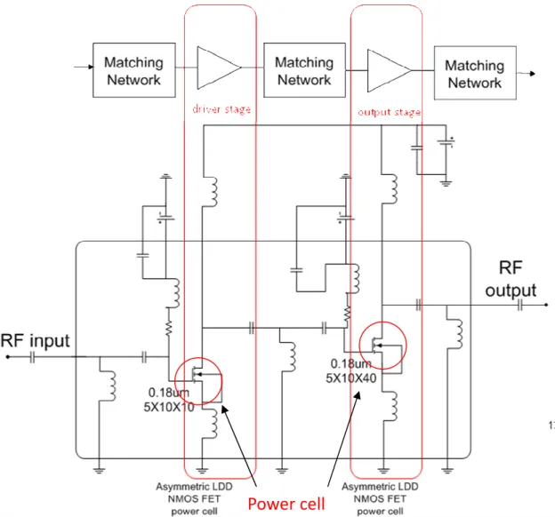
In this work, the 2-stage PA adopts a class A operation for driver stage and a class
AB for power stage. Such arrangement is optimized for gain and efficiency with good
linearity. The simplified schematic of the circuit is shown in Fig. 2.1. To consider the
power efficiency issue, the size ratio of driver stage to power stage is 1:4. Besides,
the circuit is designed with on-chip matching. Here the impedance of input,
inter-stage and output matching to transistors are carefully selected to get a
compromise between power, efficiency from load and source pull simulation.
In both stages, asymmetric-LDD MOS transistors have been implemented by
foundry standard 0.18µm 1P6M process with only one additional mask but without process modification. The unit cell designed in this work has 10 gate fingers, 0.18 µm gate length and 5 µm width. The BSIM3 model of asymmetric-LDD MOS transistor has been used in PA design, which was confirmed by on-wafer power
characterization measurements at 2.4 GHz using an ATN load-pull system. The
number of unit cell for the driver and power stage was determined by considering
- 9 -
has been carried out through the iteration of ADS and EM simulation.
Fig. 2.1 schematic of the two stage amplifier circuit
- 10 -
2.2 Pre-layout simulation process
Ideal lump model design:
First, we have to make a goal table [Table.2.1] and find out the drain bias of power
cell.
Fig. 2.2 Id-Vd analysis or the a-LDD MOSFET
From the breakdown analysis [Fig.2.2] , The I – V curve show that the breakdown with supply VGS voltage is about 5 V, breakdown without supply VGS voltage is about
7 V. So the optimum DC Vds is about 2.5 to 3V with class A operation. Then, the
- 11 -
performance of the structure with ideal result.
table 2.1 shows our goals:
Index Typical value Goal value
Output power@P1dB 10 ~ 20dBm >20dBm
PAE 10 ~ 30% >30%
Power gain 8~15dB >20dB
ACPR@15dBm < -30dBc >-40dBc
Supply voltage 1.8V >1.8
First stage design:
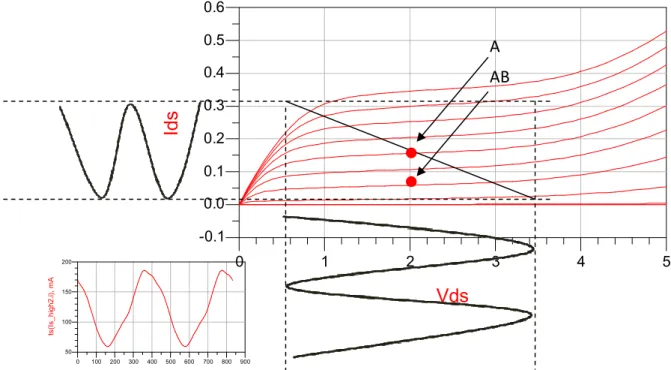
To be the first stage, the linearity and gain is the most important index, so first stage
drives in class A operation with Vgs = 1.0V. full swing generate sin wave with good
linearity but poor efficiency. Fig.2.3 show up the bias of class A and output loading
current.
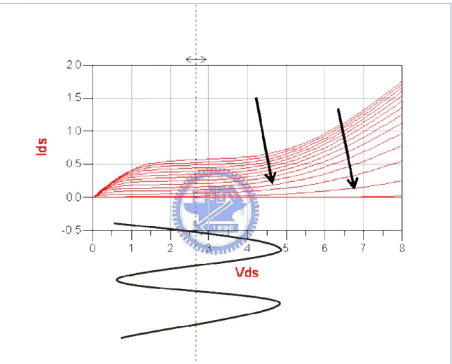
Second stage design:
The second stage, PAE and output power is the most important index, so it drives in
class AB operation with Vgs = 0.7V. by trade of linearity and efficiency, Fig.2.4 shows
that when output swing larger than about 3.2V, the current cut off and save the
- 12 - 1 2 3 4 0 5 0.0 0.1 0.2 0.3 0.4 0.5 -0.1 0.6
Vds
Id
s
Fig. 2.3 Id-Vd analysis and simulation with load line, gate voltage consideration
1 2 3 4 0 5 0.0 0.1 0.2 0.3 0.4 0.5 -0.1 0.6
Vds
Id
s
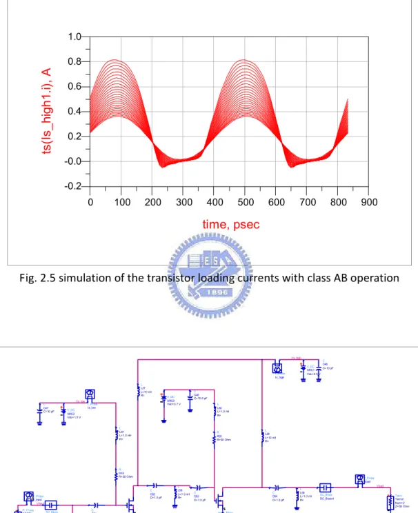
Fig. 2.4 Id-Vd analysis and simulation with class AB operation A AB 100 200 300 400 500 600 700 800 0 900 100 150 50 200 time, psec ts (I s _ h ig h 2 .i ), m A 100 200 300 400 500 600 700 800 0 900 0 200 400 600 -200 800 time, psec ts (I s _ h ig h 1 .i ), m A
- 13 -
The goal of output power is 25dBm, Vdd is about 2.5V, with Vgs 0.7V power added efficiency is about 35%. By equation, determinate output load for initial estimation. We have transistor loading current.[Fig.2.5]
100 200 300 400 500 600 700 800 0 900 -0.0 0.2 0.4 0.6 0.8 -0.2 1.0 time, psec ts (I s _ h ig h 1 .i ), A
Fig. 2.5 simulation of the transistor loading currents with class AB operation
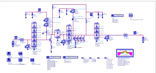
Vinput Vs_high Vload Vs_low DC_Block DC_Block3 P_1Tone PORT1 Freq= RFfreq P= dbmtow(Pavs) Z= Z_s Num= 1 I_Probe I_input C C81 C=1.0 pF L L56 R= L= 1.0 nH R R20 R=50 Ohm L L60 R= L=1.0 nH C C46 C= 10 pF I_Probe Is_high V_DC SRC1 Vdc= 2.5 V L L27 R= L=10 nH I_Probe Iload Term Term2 Z=50 Ohm Num= 2 DC_Block DC_Block4 L L59 R= L=1.0 nH C C84 C= 1.0 pF L L58 R= L= 1.0 nH C C83 C= 1.0 pF C C82 C= 1.0 pF R R19 R= 50 Ohm L L57 R= L=1.0 nH I_Probe Is_low L L14 R= L= 0.1 nH C C47 C=10 pF asym_50um Q4 C C48 C= 10.0 pF L L26 R= L=10 nH V_DC SRC3 Vdc= 0.7 V V_DC SRC2 Vdc= 1.0 V L L44 R= L= 0.2 nH asym_50um Q3
- 14 - Vs _high Vinput Vs _low Vload Simulation Control IP3out ipo1 ipo1=ip3_out( v out,{1,0},{2,-1} ,50) P0 Pin IP3out S_Param SP1
C alc N ois e=y es Step=10 MH z Stop=10.0 GHz Start=0.1 GHz S-PARAMETERS TSMC _CM018R F_PROC ESS TSMC _CM018R F_PROC ESS
R es is tanc e=Ty pic al C orner Cas e_3p3M=TT_3M C orner Cas e_1p8M=TT_M C orner Cas e_3p3N A=TT_3VN A C orner Cas e_1p8N A=TT_N A C orner Cas e_33=TT_3V C orner Cas e_18=TT
Si - Subs tr ate TSMC RF CMOS 0.18um VAR VAR 2 Z_s _5 = 50 + j*0 Z_s _4 = 50 + j*0 Z_s _3 = 50 + j*0 Z_s _2 = 50 + j*0 Z_s _fund = 50 + j*0 Z_l_5 = 5 + j*0 Z_l_4 = 5 + j*0 Z_l_3 = 5 + j*0 Z_l_2 = 5 + j*0 Z_l_fund = 5 + j*0 Eq nVa r VAR gl ob al VAR1 Eqn Va r VAR global VAR6 f_4 = 4.5* RFfreq f_3 = 3.5* RFfreq f_2 = 2.5* RFfreq f_1 = 1.5* RFfreq Eqn Var VAR VAR 3 Vpus h=2.5 Max Order=10 Pav s =Par am1 R Ffreq=2.4 GH z
Eqn Var
Har monic Balanc e
HB1 Or der[1]=Max Order Freq[1]=R Ffreq HARMONIC BALANCE ParamSweep Sweep1 Step=0.5 Stop=30 Star t=- 20 SimIns tanc eN ame[6]= SimIns tanc eN ame[5]= SimIns tanc eN ame[4]= SimIns tanc eN ame[3]= SimIns tanc eN ame[2]= SimIns tanc eN ame[1]="H B1" SweepVar ="Param1" PARAMETER SWEEP TSMC 018RF_MIMC AP C 77 C s =951.6 fF w t=30.0 um lt=30.0 um Ty pe=MiM w ith s hie ld
TSMC 018RF_MIMC AP
C 79
C s =951.6 fF w t=30 um lt=30 um Ty pe=MiM w ith s hie ld
TSMC_C M018RF_IN DS2_STD L50 lay =6 rad=70 um nr=2.75 w =15 um StabFac t StabFac t1 StabFac t1=s tab_fac t(S) StabFact Mu Mu1 Mu1=mu( S) Mu MuPrime MuPrime1 MuPrime1=mu_prime(S) MuPrime GaC irc le
GaC irc le1
GaC irc le1=ga_c ir c le( S,20,51)
GaCircle
Ns C irc le
Ns C irc le1
Ns C irc le1=ns _c ir c le( nf2,N Fmin,Sopt,R n/50,51)
NsCircle V_D C SR C 1 Vdc =2.5 V TSMC _C M018R F_IND S2_STD L55 lay =6 rad=30 um nr=0.5 w=6 um as y m_50um Q3 TSMC_C M018RF_IN DS2_STD L49 lay =6 rad=30 um nr=2.5 w =6 um TSMC _C M018R F_IND S2_STD L54 lay =6 rad=30 um nr=0.5 w=6 um TSMC_C M018RF_IN DS2_STD L48 lay =6 rad=35 um nr=2.5 w =15 um TSMC 018RF_MIMC AP C 70 C s =670.5 fF w t=21 um lt=30 um Ty pe=MiM w ith s hield
TSMC_C M018RF_IN DS2_STD L53 lay =6 rad=40 um nr=3.5 w =15 um TSMC018R F_MIMC AP C 81 C s =951.6 fF w t=30.0 um lt=30.0 um Ty pe=MiM with s hield
TSMC018R F_MIMC AP
C 84
C s =951.6 fF w t=30.0 um lt=30.0 um Ty pe=MiM with s hield
TSMC018R F_MIMC AP
C 86
C s =951.6 fF w t=30.0 um lt=30.0 um Ty pe=MiM with s hield
TSMC018R F_MIMC AP
C 85
C s =951.6 fF w t=30.0 um lt=30.0 um Ty pe=MiM with s hield
TSMC018R F_MIMC AP
C 83
C s =951.6 fF w t=30.0 um lt=30.0 um Ty pe=MiM with s hield
TSMC018R F_MIMC AP
C 82
C s =951.6 fF w t=30.0 um lt=30.0 um Ty pe=MiM with s hield
L L44 R = L=0.2 nH DC _Bloc k DC _Bloc k 3 TSMC 018RF_MIMC AP C 78 C s =951.6 fF w t=30.0 um lt=30.0 um Ty pe=MiM w ith s hie ld
TSMC 018RF_MIMC AP
C 76
C s =951.6 fF w t=30.0 um lt=30.0 um Ty pe=MiM w ith s hie ld
L L27 R= L=10 nH TSMC 018R F_MIMCAP C75 Cs =951.6 fF wt=30.0 um lt=30.0 um Ty pe=MiM w ith s hield
TSMC 018R F_MIMCAP
C74
Cs =951.6 fF wt=30.0 um lt=30.0 um Ty pe=MiM w ith s hield
TSMC 018R F_MIMCAP
C73
Cs =951.6 fF wt=30.0 um lt=30.0 um Ty pe=MiM w ith s hield
TSMC 018R F_MIMCAP
C72
Cs =951.6 fF wt=30.0 um lt=30.0 um Ty pe=MiM w ith s hield
TSMC 018RF_MIMC AP
C 71
C s =670.5 fF w t=21 um lt=30.0 um Ty pe=MiM w ith s hield
V_D C SR C2 Vdc =1.0 V V_D C SR C3 Vdc =0.7 V D C _Bloc k D C _Bloc k 4 L L26 R = L=10 nH I_Pr obe Is _high C C 46 C =10 pF TSMC_C M018RF_R ES_R F R 18 R =50.72 Ohm l=13 um w =2 um
Ty pe=P+ Poly w /i s ilic ide (0.18<=w <=5.0) (R F)
C C48 C=10.0 pF as y m_50um Q7 as y m_50um Q6 as y m_50um Q5 as y m_50um Q4 C C 47 C =10 pF Term Term2 Z=50 Ohm N um=2 I_Probe Iload TSMC _C M018R F_R ES_RF R17 R=50.72 Ohm l=13.001 um w=2 um
Ty pe=P+ Poly w/i s ilic ide (0.18<=w<=5.0)( RF)
L L14 R = L=0.1 nH I_Pr obe Is _low P_1Tone POR T1 Fr eq=RFfreq P=dbmtow( Pav s ) Z=Z_s N um=1 I_Probe I_input
Fig. 2.7 tsmc model schematic
After finding out the value of passive components, replace with tsmc models [Fig.2.7],
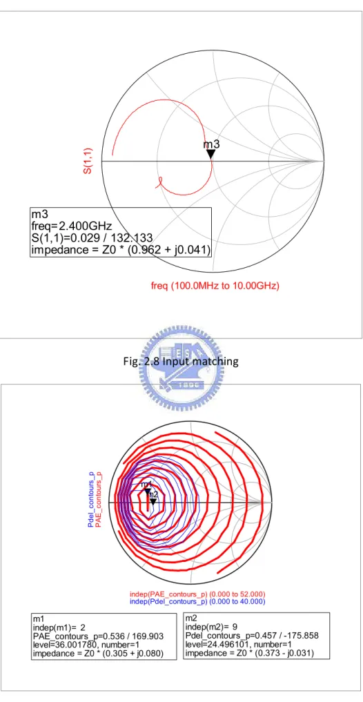
finishing the input matching task [Fig.2.8 ], and trade off output power to PAE on the
load pull simulation system. Fig.2.9 show that constant PAE circle and constant
output power circle, we take the point as the loading impedance between the central
point of maximum constant output power circle and maximum constant PAE circle.
After that, check the stability factor, make sure it is larger than 1[Fig.2.10], and check
the s-parameter prevent oscillation. and the small signal gain larger than 20dB [2.11]
At last, make sure every small signal and large signal within the goal and it was in the
- 15 - freq (100.0MHz to 10.00GHz) S (1 ,1 ) m3 m3 freq= S(1,1)=0.029 / 132.133 impedance = Z0 * (0.962 + j0.041) 2.400GHz
Fig. 2.8 Input matching
indep(PAE_contours_p) (0.000 to 52.000) P A E _ c o n to u rs _ p m1 indep(Pdel_contours_p) (0.000 to 40.000) P d e l_ c o n to u rs _ p m2 m1 indep(m1)= PAE_contours_p=0.536 / 169.903 level=36.001780, number=1 impedance = Z0 * (0.305 + j0.080) 2 m2 indep(m2)= Pdel_contours_p=0.457 / -175.858 level=24.496101, number=1 impedance = Z0 * (0.373 - j0.031) 9
- 16 - 2 4 6 8 0 10 0.833 1.667 2.500 3.333 4.167 0.000 5.000 freq, GHz M u 1 m5 m9 m10 M u P ri m e 1 m12 S ta b F a c t1 m5 freq= Mu1=1.344 970.0MHz m9 freq= Mu1=1.423 5.230GHz m10 freq= Mu1=1.098 Min 100.0MHz m12 freq= MuPrime1=1.360 10.00GHz
Fig. 2.10 stability factor > 1
2 4 6 8 0 10 -100 -50 0 -150 50 freq, GHz d B (S (2 ,1 )) m6 d B (S (1 ,1 )) m13 d B (S (2 ,2 )) m11 m6 freq= dB(S(2,1))=23.696 2.400GHz m11 freq= dB(S(2,2))=-7.819 2.400GHz m13 freq= dB(S(1,1))=-30.895 2.400GHz Fig. 2.11 s-parameter of S11 –S21.
- 17 -
After simulation and match the goal, we run the layout flow to implement the chip.
Fig. 2.12 show the layout topology, input power comes from the left and
symmetrically to two power cells, the signal enlarge in fist stage, after internal
matching circuit, the signal drive the second stage with fish bond symmetric wire and
combine with output matching network.
Fig. 2.12 the layout before post layout simulation
INPUT OUTPUT BIAS BIAS GND GND GND GND GND GND GND IND BW IND BW GND
- 18 -
2.3 Post-layout simulation
Fig. 2.13 Export the line of layout to momentum ADS system and simulation
Layout is also a very important task for power amplifier design, due to the
intersection influence or parasitic, the chip performance cannot match the design in
practical, so we have to decrease those effects by post-layout simulation process.
Fig.2.13 show the critical DC power line generates parasitic resistance [Fig.2.13 red
circle]. To prevent loss, the line has to be widened. After modify the layout simulate
- 19 - Vs _h ig h Vlo ad Vin put I_Pro be Is _ lo w V_ DC SRC2 Vd c =1 .0 V V_ DC SRC1 Vd c =2 .5 V I_Prob e Is _h ig h C C46 C=1 0 pF DC_Blo c k DC_Blo c k 4 I_ Probe Il oa d T erm T erm 2 Z =50 Ohm Num =2 PA_p os i m 1 PA_p os i m 1_ 1 M o del Ty pe= M W IP3ou t ip o1
ip o1= ip 3_o ut(v out,{1 ,0 },{2,-1 },50 )
P P I P3out S_Param SP1 Cal c Noi s e= y es Step= 0.1 GHz Stop= 10.0 GHz Start= 0.1 GHz S-PARAM ETERS T SM C_ CM 01 8RF _PROCESS T SM C_ CM 01 8RF _PROCESS Res i s tan c e= Ty p ic al CornerCa s e_ 3p3 M =TT _3M CornerCa s e_ 1p8 M =TT _M CornerCa s e_ 3p3 NA= TT_ 3VNA CornerCa s e_ 1p8 NA= TT_ NA CornerCa s e_ 33= TT_ 3V CornerCa s e_ 18= TT Si - Subs trate TSMC RF CMOS 0.18um VAR VAR2 Z _s _ 5 = 50 + j *0 Z _s _ 4 = 50 + j *0 Z _s _ 3 = 50 + j *0 Z _s _ 2 = 50 + j *0 Z _s _ fu nd = 50 + j *0 Z _l _5 = 5 + j *0 Z _l _4 = 5 + j *0 Z _l _3 = 5 + j *0 Z _l _2 = 5 + j *0 Z _l _fund = 5 + j *0 Eqn Var VAR VAR3 Vpu s h= 2.5 M ax Ord er=10 Pav s =Param 1 RFfreq= 2.4 GHz Eqn Var VAR global VAR6 f _4 = 4. 5* RFf r eq f _3 = 3. 5* RFf r eq f _2 = 2. 5* RFf r eq f _1 = 1. 5* RFf r eq Eqn Var VAR global VAR1 Eqn Var Ha rm o ni c Ba la nc e HB1 Orde r[1]=M a x Orde r Freq [1 ]= RFfreq
HARM ONIC BALANCE
Pa ra m Swe ep
Sweep 1
Step =1 Stop =10 Start=-10 Si m Ins tan c eNam e[6]= Si m Ins tan c eNam e[5]= Si m Ins tan c eNam e[4]= Si m Ins tan c eNam e[3]= Si m Ins tan c eNam e[2]= Si m Ins tan c eNam e[1]="HB1" Sweep Var="Pa ra m 1"
PARAM ETER SWEEP
M u M u 1 M u 1=m u (S) M u Ns Ci rc l e Ns Ci rc l e1 Ns Ci rc l e1= ns _ c i rc le (n f2 ,NFm i n,Sop t,Rn /5 0,51) NsCir cle Stab Fac t Stab Fac t1
Stab Fac t1 =s tab _fac t(S)
St abFact
GaCirc l e
GaCirc l e1
GaCirc l e1 =ga _c i rc l e(S,20,51 )
G aCircle
M u Prim e
M u Prim e 1
M u Prim e 1=m u _pri m e(S)
M uPrim e TSM C018 RF_ M IM CAP C10 0 Cs = 951 .6 fF wt=30 .0 u m lt=3 0.0 um Ty p e=M i M wi th s hi el d TSM C01 8RF_M IM CAP C9 4 Cs =32 6.9 fF wt=1 0 um l t= 30 um Ty pe= M iM with s h ie ld TSM C01 8RF_M IM CAP C9 2 Cs =32 6.9 fF wt=1 0 um l t= 30 um Ty pe= M iM with s h ie ld T SM C0 18RF_M IM CAP C93 Cs =3 26.9 fF wt= 10 um l t=30 u m T y pe =M i M with s h ie ld as y m _5 0um Q1 5 as y m _5 0um Q8 as y m _5 0um Q9 as y m _50 um Q10 TSM C01 8RF _M IM CAP C9 1 Cs =95 1.6 fF wt=3 0.0 um l t= 30.0 um Ty pe= M iM wi th s hi el d TSM C01 8RF _M IM CAP C9 0 Cs =95 1.6 fF wt=3 0.0 um l t= 30.0 um Ty pe= M iM wi th s hi el d TSM C018 RF_ M IM CAP C89 Cs = 951 .6 fF wt=30 .0 u m lt=3 0.0 um Ty p e=M i M wi th s hi el d TSM C01 8RF _M IM CAP C7 2 Cs =95 1.6 fF wt=3 0.0 um l t= 30.0 um Ty pe= M iM wi th s hi el d TSM C_CM 018 RF_ INDS2 _ST D L4 8 l ay = 6 rad= 35 um nr=2 .5 w= 15 um L L27 R= L=1 0 nH TSM C018 RF_ M IM CAP C99 Cs = 670 .5 fF wt=21 u m lt=3 0 um Ty p e=M i M wi th s hi el d TSM C018 RF_ M IM CAP C70 Cs = 670 .5 fF wt=21 u m lt=3 0 um Ty p e=M i M wi th s hi el d as y m _50 um _h al f Q14 as y m _50 um _h al f Q13 C C4 7 C= 10 pF TSM C01 8RF _M IM CAP C8 1 Cs =95 1.6 fF wt=3 0.0 um l t= 30.0 um Ty pe= M iM wi th s hi el d TSM C01 8RF _M IM CAP C8 3 Cs =95 1.6 fF wt=3 0.0 um l t= 30.0 um Ty pe= M iM wi th s hi el d TSM C01 8RF _M IM CAP C8 2 Cs =95 1.6 fF wt=3 0.0 um l t= 30.0 um Ty pe= M iM wi th s hi el d TSM C01 8RF _M IM CAP C9 8 Cs =95 1.6 fF wt=3 0.0 um l t= 30.0 um Ty pe= M iM wi th s hi el d TSM C01 8RF _M IM CAP C9 7 Cs =95 1.6 fF wt=3 0.0 um l t= 30.0 um Ty pe= M iM wi th s hi el d TSM C01 8RF _M IM CAP C9 6 Cs =95 1.6 fF wt=3 0.0 um l t= 30.0 um Ty pe= M iM wi th s hi el d TSM C_CM 018 RF_ INDS2 _ST D L5 5 l ay = 6 rad= 30 um nr=0 .5 w= 6 um TSM C_CM 018 RF_ INDS2 _ST D L5 4 l ay = 6 rad= 30 um nr=0 .5 w= 6 um TSM C_CM 018 RF_ RES_RF R1 7 R= 50.72 Ohm l =13 .0 01 um w= 2 um Ty pe= P+ Po ly w/i s i li c i de (0.18 <=w<=5 .0 )(RF ) TSM C_CM 0 18RF_INDS2_ STD L53 la y =6 ra d=4 0 um nr=3.5 w=1 5 um DC_Blo c k DC_Blo c k 3 P_ 1To ne PORT1 Freq =RF freq P= dbm tow(Pav s ) Z= Z_s Nu m =1 I_Pro be I_i np ut TSM C_CM 018 RF_ RES_RF R1 8 R= 50.72 Ohm l =13 u m w= 2 um Ty pe= P+ Po ly w/i s i li c i de (0.18 <=w<=5 .0 )(RF ) V_ DC SRC3 Vd c =0 .7 V C C4 8 C= 10.0 pF TSM C_CM 01 8RF _INDS2_STD L5 6 l ay = 6 rad= 70 um nr=2 .7 5 w= 15 um L L2 6 R= L= 10 nH T SM C_ CM 01 8RF _INDS2_STD L 49 l ay =6 rad =30 u m n r= 2.5 w=6 um
Fig.2.14 post layout simulation with line calculation
To modify the layout with better simulation result, I use ADS momentum system to
generate wire model and use ADS to simulate the result with wire model. [Fig.2.14]
In this way, we can figure out the influence of wire effect. After this task, I can
determinate the best layout topology and tape out. With the simulation, Fig. 2.15
show the final layout version with best result, Fig. 2.16 show the photograph of the
- 20 -
Fig. 2.15 the layout after post layout simulation.
- 21 -
Chapter 3
SIMULATION AND MEASUREMENT RESULT
To verify the chip design, we first measured the small signal S-parameters. Fig. 3.1
shows the on-wafer measurement data, which show a 20 dB gain and 17 dB input
and output return loss- this is consistence with EM post-simulation data.
1
2
3
4
5
6
7
8
-40
-30
-20
-10
0
10
20
S11 S22 S21 Symbol:measured data Line: modeled datad
B
Frequency (GHz)
Fig. 3.1. Measured and simulated gain and return loss for CMOS PA.
Fig. 3.2 shows the measured RF power results of the amplifier. The output power
at 1 dB compression (P1dB) increases with increasing bias voltage from conventional
- 22 -
simulation. Under 2.5 V bias operation, a P1dB of 20.8 dBm and power gain of 20 dB
are measured with 30% PAE. The P1dB increases to 21.5 dBm at higher 2.75V bias
condition with still compatible 19.6 dB power gain and 29.6% PAE.
Good adjacent channel power ratio (ACPR) is an important linearity factor for PAs.
Fig. 3.3 shows the measured ACPR with standard W-CDMA π/4 QPSK modulation on
different bias voltage. Here the ACPR improves with increasing operation voltage
from 1.8, 2.5 to 2.75V monotonically. At the 2.75 V bias voltage, an ACPR of -56 dBc
at 0 dBm output power or -30 dBc at 20 dBm output power was measured, which is
competitive to the data of the power amplifiers designed for better linearity [15]. In
addition, IP3 point is an important factor, the Fig.3.4 ~ Fig.3.6 show up the IP3 point
with different supply voltage. The output IP3 point of 1.8V, 2.5V and 2.75V is 22dBm,
26dBm and 36dBm. So it shows that the linearity increases with larger supply
- 23 - -10 -5 0 5 10 8 10 12 14 16 18 20 22 24 measurement 2.5V measurement 2.75V simulation 2.5V simulation 2.75V O u tp u t P o w e r (d B m ) Input Power (dBm) P o w e r-A d d e d E ff ic ie n c y ( % ) G a in ( d B ) 0 10 20 30 40 50 60
Fig. 3.2. Measured and simulated RF output power, gain and PAE of designed PA using high breakdown voltage asymmetric-LDD MOSFETs.
-10 0 10 20 -60 -40 -20 A C P R ( d B c ) OUTPUT POWER (dBm) VDD =1.8V VDD = 2.5V VDD = 2.75V fi Fig. 3.3. Measured ACPR of designed PA using high breakdown voltage
- 24 - -12 -10 -8 -6 -4 -2 0 2 4 6 8 10 12 -50 -40 -30 -20 -10 0 10 20 30
O
U
T
P
U
T
P
O
W
E
R
(
d
B
m
)
INPUT POWER (dBm)
fund
IM3
IM5
Fig. 3.4 measurement data of third order inter modulation with 1.8V supply voltage.
-12 -10 -8 -6 -4 -2 0 2 4 6 8 10 12 -50 -40 -30 -20 -10 0 10 20 30
O
U
T
P
U
T
P
O
W
E
R
(
d
B
m
)
INPUT POWER (dBm)
fund
IM3
IM5
- 25 - -30 -25 -20 -15 -10 -5 0 5 10 15 20 -100 -90 -80 -70 -60 -50 -40 -30 -20 -10 0 10 20 30 40
O
U
T
P
U
T
P
O
W
E
R
(
d
B
m
)
INPUT POWER (dBm)
fund IM3 IM5Fig. 3.6 measurement data of third order inter modulation with 2.75V supply voltag
Chapter 4
COMPARISON
The die photo of fabricated CMOS PA is shown in Fig. 2.16, which has a chip area of
1m×1.1m. Table 4.1 summarizes the performance comparison with reported CMOS
PA [10]-[16]. The fabricated PA using high breakdown voltage asymmetric-LDD
MOSFETs shows the large P1dB of 21.5 dBm, high gain of 20.4 dB, and good 29.6%
PAE at 2.4 GHz. Those power performances are better than other reported designs
shown in Table 4.1, with added merits of simple single-ended design, using standard
- 26 -
Table 4.1 The comparison table of Asymmetry MOS and conventional PAs.
Ref. Freq.
(GHz) voltage Pout (dBm) Gain (dB) PAE (%)
Width/Pow er density by P1dB(W/m m) Matchin g technolog y [10] 5 1.8 19.2@1dB 7.1 17.5 1.28mm/0.065 On chip 0.18um [11] 5.2 1.8 17.4/15.4@1 dB 15.1 27.1 0.6mm/0.058 On chip 0.18um [12] 5.8 1 20.5@1dB ~8 27 (Drain) 9.6mm/0.012 On chip 90nm [13] 2.4/5.2 1.8 [email protected] [email protected] [email protected] z [email protected] [email protected] GHz 1.92mm/0.046 On chip 0.18um [14] 3.7~8. 8 1.8 19 15.6@1dB 8.24 25 0.96mm/0.038 On chip 0.18um
[15] 2~2.45 2.5 16.3@1dB 18 --- 4.2mm/0.01 Off chip 0.13um
[16] 2.4 2.5 20@1dB 11.2 28 0.96mm/0.1 Off chip 0.25um
This work 2.4 2.5 22.7 20.8@1dB 20 30 2mm/0.071 On chip 0.18um 2.75 23.2 21.5@1dB 19.6 29.6
- 27 -
Chapter 5
CONCLUSION
We have designed an asymmetric-LDD MOS transistor which has ~twice drain
breakdown voltage to the conventional one. Besides, the power amplifier has been
designed by single ended on chip design and fabricated by TSMC 0.18um 1P6M
process without any process modification. The excellent power performance shows
20dB power gain, and 20.8dBm P1dB compression power and 22.7dBm saturate
output power with 30% PAE under 2.5V bias operation. And 20.4dB power gain,
21.5dBm P1dB compression power and 23.2dBm saturate output power with 29.6%
PAE under 2.75V bias operation. -41dBc ACPR at 15dBm output power, ~36dBm OIP3
with 2.75V supply voltage. The output power and linearity increase with larger
supply voltage, and PAE and power gain saturate at 2.75V. This research
demonstrated that the asymmetric-LDD MOS transistor successfully implemented on
a CMOS power amplifier with wonderful performance even with on chip matching
design. This design method has great opportunity to be future trend and realize SOC
- 28 -
REFERENCE
[1] J.C. Guo, C. H. Huang, K. T. Chan, W. Y. Lien, C. M. Wu, and Y. C. Sun, “0.13μm low
voltage logic base RF CMOS technology with 115GHz fT and 80GHz fMax ” 33rd
European Microwave Conference, pp. 682-686, 2003.
[2] “How Bluetooth Technology Works”. Bluetooth SIG. Retrieved on 2008-02-01.
[3] M. C. King, T. Chang, and A. Chin “RF Power Performance of Asymmetric-LDD MOS
Transistor for RF-CMOS SOC Design”, IEEE MICROWAVE AND WIRELESS COMPONENTS
LETTERS, VOL. 17, NO. 6, JUNE 2007. pp. 445 – 447.
[4] J. F. Chen J. Tao, P. Fang, and C. Hu, ” 0.35- m Asymmetric and Symmetric LDD Device
Comparison Using a Reliability/Speed/Power Methodology”, IEEE ELECTRON DEVICE
LETTERS, VOL. 19, NO. 7, JULY 1998. pp. 216-218.
[5] G. Krieger, R. Sikora, P. Cuevas, and M. Misheloff, “Moderately doped NMOS
(M-LDD)—hot electron and current drive optimization,” IEEE Trans. Electron Devices, vol. 38, p. 121, Jan. 1991.
[6] T. H. Lee, H. Samawati, and H. R. Rategh, “5-GHz CMOS wireless LANs,” in IEEE
Transaction Microwave Theory and Technique, vol. 50, 2002, pp. 268-280.
[7] E. Chen, D. Heo, M. Hamai, J. Laskar, and D. Bien, “0.24-um CMOS technology for
Bluetooth power applications,” in Proc. IEEE Radio and Wireless Conference, 2000, pp. 163-166.
[8] A. Litwin, O. Bengtsson, and J. Olsson, “Novel BiCMOS compatible, short channel
LDMOS technology for medium voltage RF and power applications,” in IEEE MTT-S
International Microwave Symposium Dig., 2002, pp.35-38.
[9] K.-E. Ehwald, B. Heinemann, W. Roepke, W. Winkler, H. Rücker, F. Fuernhammer, D.
Knoll, R. Barth, B. Hunger, H. E. Wulf, R. Pazirandeh, and N. Ilkov, “High performance RF LDMOS transistors with 5 nm gate oxide in a 0.25m SiGe:C BiCMOS technology,” in
IEDM Tech. Dig., 2001, pp. 40.4.1-40.4.4.
[10] Y. Eo and K. Lee, “High efficiency 5 GHz CMOS power amplifier with adaptive bias control circuit,” 2004 IEEE RFIC Symp. Dig., Fort Worth, TX, June 2004, pp. 575-578.
- 29 -
[11] W. Zhang, E.-S. Khoo, and T. Tear, “A low voltage fully-integrated 0.18um CMOS power amplifier for 5GHz WLAN ,” Proc. 28th European Solid-State Circuits Conf., Florence, Italy, Sep. 2002, pp. 215-218.
[12] P. Haldi, D. Chowdhury, G. Liu and A. M. Niknejad , “A 5.8 GHz Linear Power Amplifier in a Standard 90nm CMOS Process using a 1V Power Supply,” in IEEE Radio Frequency
Integrated Circuits Symp., 2007, pp.431-434.
[13] Y. Eo, and K. Lee, “ A 2.4GHz/5.2GHz CMOS power amplifier for dual-band applications,” 2004 IEEE MTT-S Int. Microwave Symp. Dig., Fort Worth, TX, June 2004, vol. 3, pp. 1539-1542.
[14] C. Lu, A-V. H. Pham, M. Shaw, and C. Saint “Linearization of CMOS Broadband Power Amplifiers through Combined Multi-gated Transistors and Capacitance Compensation”
IEEE Transaction On Microwave Theory And Techniques. Nov. 2007 pp. 2320-2328
[15] V. Knopik, B. Martineau, and D. Belot, “20 dBm CMOS class AB power amplifier design for low cost 2 GHz-2.45 GHz consumer applications in a 0.13μm technology,” Proc. IEEE
Int. Symp. Circuits and Systems, Kobe, Japan, May 2005, vol. 3, pp. 2675-2678.
[16] C.-C. Yen, and H.-R. Chuang “A 0.25-µm 20-dBm 2.4-GHz CMOS Power Amplifier with an Integrated Diode Linearizer,” in IEEE Microwave & Wireless Components Letter, vol. 13, no. 2, 2003, pp45-47