國 立 交 通 大 學
電信工程學系
碩 士 論 文
低溫共燒陶瓷技術之串聯架構帶通濾波器
暨射頻前端天線切換模組的研究
Research on Band-pass Filter of Serial Configuration and
RF Front-End Antenna Switch Module Using LTCC
研 究 生:張鈞富
(Chun-Fu Chang)
指導教授:鍾世忠 博士
(Dr. Shyh-Jong Chung)
低溫共燒陶瓷技術之串聯架構帶通濾波器
暨射頻前端天線切換模組的研究
Research on Band-pass Filter of Serial Configuration and
RF Front-End Antenna Switch Module Using LTCC
研 究 生:張鈞富 Student: Chun-Fu Chang
指導教授:鍾世忠 博士 Advisor: Dr. Shyh-Jong Chung
國立交通大學
電信工程學系碩士班
碩士論文
A Thesis
Submitted to Department of Communication engineering
College of Electrical and Computer Engineering
National Chiao Tung University
In Partial Fulfillment of the Requirements
For the Degree of
Master of Science
In
Communication Engineering
June 2006
HsinChu, Taiwan, Republic of China
低溫共燒陶瓷技術之串聯架構帶通濾波器
暨射頻前端天線切換模組的研究
研 究 生:張鈞富 指導教授:鍾世忠 博士
國立交通大學電信工程學系
摘要
本篇論文前段旨在利用低溫共燒陶瓷多層架構的技術,設計一串聯架構 的帶通濾波器。別於以往傳統帶通濾波器利用耦合傳輸線架構的濾波器跨接 一耦合電容形成一迴授路徑來產生有限傳輸零點;此串聯架構帶通濾波器乃 是利用傳統耦合傳輸線架構的濾波器串接一個對地的電容,藉以形成一迴授 路徑,因此而產生有限傳輸零點。改變此對地電容之容值,便可以控制有限 傳輸零點的頻率,並且不影響通帶的頻率響應特性。此帶通濾波器適用於藍 牙或無線區域網路(IEEE 802.11b/g)之應用中。 在本篇論文的後段,則是利用低溫共燒陶瓷技術來設計一射頻前端天線 切換模組,此模組把主動元件、被動元件以及內嵌式天線整合起來,形成一 系統封裝之射頻前端模組。被動電路以及天線的部分都是內埋在低溫共燒陶 瓷的基板裡面,主動元件則是黏著在基板的表面上,再利用磅線把內埋的被 動元件與主動元件連結起來。因此在設計上,必須將磅線的影響加以考慮。 由於磅線在高頻的時候近乎等效成電感,對於內埋的被動電路而言,輸入阻 抗的匹配會被磅線破壞,所以整體的頻率響應會受磅線所影響。本篇論文把 此磅線的效應加以考慮並利用磅線近似電感的現象設計所有內埋的被動電路 與天線,讓此前端天線模組具有體積小、全向性輻射場型、以及被動電路特 性良好之特色,頻段適合於無線區域網路(IEEE 802.11a)的應用中。Research on Band-pass Filter of Serial Configuration and
RF Front-End Antenna Switch Module Using LTCC
Student: Chun-Fu Chang Advisor: Dr. Shyh-Jong Chung
Department of Communication Engineering
National Chiao Tung University
Abstract
In front of this thesis, a band-pass filter of serial configuration using Low Temperature Co-fired Ceramic (LTCC) technology is proposed and designed. Different from the conventional band-pass filter, which uses a coupling capacitor between two I/O ports to form a feedback path and thus can generate finite transmission zeros; the proposed band-pass filter is based on an architecture of a conventional coupled-line filter, and incorporates a grounding capacitor to form the feedback path. By changing the value of the grounding capacitor, we can control the frequencies of the finite transmission zeros without affecting the frequency response of the pass band. The proposed band-pass filter which has low insertion loss at pass band can be applied in Bluetooth or IEEE 802.11b/g WLAN (Wireless Local Area Network).
Additionally, we propose and design a RF front-end antenna switch module, which integrates an active component, two passive components, and an embedded antenna into a RF front-end System-on-Package (SOP). The passive circuits and the antenna are buried in the LTCC substrate, while the active component is mounted on the top surface of the substrate. Thus, bond wires are thus necessary for the connection among the active component and the buried circuits/antenna. Because the bond wire is similar to the inductor at microwave frequencies, we have to take the effect of the bond wire into account, in order to avoid the bond wire affecting the input impedance of the buried circuits. In this thesis, we utilize the bond wire for compensation on the input impedance matching of buried circuits. With proper design, the module has compact size, omni-directional radiation pattern, and low insertion loss of passive circuits. The proposed antenna switch module is suitable for applications of IEEE 802.11a WLAN.
誌謝
在交大電信研究所兩年的時間,微波方面的知識收穫甚多,這真的要很 感謝鍾世忠教授的細心指導。這兩年來跟著老師做研究,學到的不只是微波、 天線方面的知識,更多的是在做人處事上的態度與方法,這些都讓我終身受 益。同時要感謝實驗室所有的成員:珮華、明潔、何博、阿信、菁偉、佩宗、 嘉言、民仲、明洲、吉佑、峰哥、克強、煥能、敦智、彥圻、崇育、明達、 光甫、彥志、旭哥、小圓、小巴、建宏、小花、淑君、玫翎、小黃,有你們 的陪伴,讓實驗室在大家專心研究之餘,還創造了許多快樂的時光,充滿很 多深刻美好的回憶。 另外,我也要感謝我的眾多同學與朋友們:阿 、雄光、尼可、中義、 雄仔、死歐、冠轟、阿魯咪、阿昇、揪尼、小南、小瑩、恒如、寶寶、小巫、 小魚、小紫。有大家的陪伴,讓我這兩年的生活更是多采多姿,謝謝你們! 最後要感謝我的家人,這些年來的鼓勵與支持,讓我可以全心全力投入 於課業上,讓我可以順利的完成研究所的學業,謝謝你們,我真的愛你們!Contents
摘要... i Abstract... ii 誌謝... iii Contents ... iv List of Figures... vList of Tables... viii
Chapter 1 Introduction... 1
Chapter 2 Band-pass Filter of Serial Configuration... 4
2.1 Theory and Design... 5
2.2 LTCC Layouts and EM Simulation ...11
2.3 Experimental Results ... 17
Chapter 3 RF Front-End Antenna Switch Module ... 21
3.1 Block Diagram of Antenna Switch Module... 22
3.2 Band-pass Filter Design... 23
3.2.1 Band-pass Filter Configuration... 23
3.2.2 EM Simulation ... 26
3.2.3 Experimental Results ... 30
3.3 Low-pass Filter Design ... 31
3.3.1 Low-pass Filter Configuration... 31
3.3.2 EM Simulation ... 34
3.3.3 Experimental Results ... 36
3.4 Embedded Antenna Design... 38
3.4.1 Antenna Structure ... 38 3.4.2 EM Simulation ... 42 3.4.3 Experimental Results ... 46 3.5 DPDT Switch Verification ... 50 3.6 Module Integration... 54 Chapter 4 Conclusions... 64 References ... 66
List of Figures
Fig. 2.1 Schema of the proposed band-pass filter of Serial Configuration... 5
Fig. 2.2 (a) Representation of the proposed filter with two serially-connected networks. (b) The upper network (Network 1). (c) The lower network (Network 2)... 7
Fig. 2.3 Mutual reactance function XU21 of the upper network (network 1) and the negative of the mutual reactance, −XL21, of the lower network (Network 2)... 8
Fig. 2.4 Scattering parameters (ideal responses) of the proposed band-pass filter with different grounding capacitances. ... 10
Fig. 2.5 3-D LTCC layout of the 2.4-GHz band-pass filter. ... 13
Fig. 2.6 EM simulated scattering parameters of the 2.4-GHz band-pass filter with and without excavated bottom ground plane. ... 14
Fig. 2.7 3-D LTCC layout of the 4.8-GHz band-pass filter. ... 15
Fig. 2.8 Scattering parameters of the 4.8-GHz band-pass filter calculated by EM simulator and circuit simulator... 16
Fig. 2.9 Comparison of the measured and EM simulated scattering parameters of the 2.4-GHz band-pass filter. ... 18
Fig. 2.10 Comparison of the measured and EM simulated scattering parameters of the 4.8-GHz band-pass filter. ... 19
Fig. 2.11 Photograph of the two fabricated LTCC filters. The photograph on the left shows the 2.4-GHz BPF, and the other shows the 4.8-GHz BPF... 20
Fig. 3.1 Side view of the bond wires connecting the bare die and buried circuits. ... 22
Fig. 3.2 Block diagram of the RF front-end antenna switch module... 23
Fig. 3.3 (a) Schema of commonly used filter with capacitors as impedance inverter (b) Schema with bond wire (c) Full-wave simulated results of (a) and (b)... 25
Fig. 3.4 Schema of the proposed band-pass filter for module integration... 26
Fig. 3.5 Side view of the bond wire’s layout. ... 27
Fig. 3.6 Comparison between the bond wire and an inductor (0.82 nH)... 27
Fig. 3.7 EM simulated and measured results without a bond wire. ... 28
Fig. 3.8 EM simulated and measured results with a bond wire. ... 28
Fig. 3.10 (a) Schema of conventionally used low-pass filter (b) Schema with a bond wire (c)
Simulation results of (a) and (b). ... 32
Fig. 3.11 Schema of the proposed low-pass filter for module integration... 33
Fig. 3.12 Ideal simulation results of the proposed low-pass filter. ... 33
Fig. 3.13 3-D layouts of the low-pass filter. ... 35
Fig. 3.14 EM simulation results of the low-pass filter... 36
Fig. 3.15 Measured results of the low-pass filter without a bond wire... 37
Fig. 3.16 Measured results of the low-pass filter with a bond wire... 38
Fig. 3.17 Structure of the inverted-F antenna. ... 40
Fig. 3.18 Equivalent transmission-line model for the inverted-F antenna... 40
Fig. 3.19 The geometry of the inverted-F antenna. (a) PCB (b) LTCC ... 41
Fig. 3.20 3-D layouts of the embedded inverted-F antenna... 43
Fig. 3.21 EM simulated return loss (S11) of the embedded inverted-F antenna... 44
Fig. 3.22 EM simulated radiation patterns at 5.3 GHz in three principal planes for the embedded inverted-F antenna. ... 45
Fig. 3.23 Measured result (S11) of the embedded inverted-F antenna. ... 47
Fig. 3.24 Measured radiation patterns in the three principal planes for the embedded inverted-F antenna. ... 48
Fig. 3.25 Outline drawing of the switch bare die (unit: um)... 50
Fig. 3.26 Photograph of the bare die measured by probes... 51
Fig. 3.27 Measured results including insertion losses and isolations of the switch... 53
Fig. 3.28 Surface wiring and layout on the top surface of the LTCC substrate... 55
Fig. 3.29 Internal layouts and grounding vias between two grounds. ... 56
Fig. 3.30 Comparison between pure antenna and antenna in the whole module... 59
Fig. 3.31 Comparison between pure BPF and BPF in the whole module. ... 59
Fig. 3.32 Comparison between pure LPF and LPF in the whole module... 60
Fig. 3.33 Isolations between antenna and filters... 60
Fig. 3.34 Isolations between BPF and LPF... 61
Fig. 3.35 EM simulated radiation patterns of the antenna with 2 filters inside the LTCC substrate. ... 62 Fig. 3.36 Comparison between EM simulated radiation patterns with and without 2 filters
List of Tables
Table 3.1 Peak and average gains of the EM simulated radiation patterns (E-Total field) at 5.2 GHz for the embedded inverted-F antenna. ... 46 Table 3.2 Measured radiation gains at each frequency in each principal plane for the embedded inverted-F antenna. ... 49
Chapter 1 Introduction
The swift development of mobile communication has made size and weight reduction, low cost and high performance essential for RF products. To make a compact design of RF passive components, such as filters, baluns, matching circuits, and even antennas, can be implemented on a multilayer stack-up substrate. Other RF active components and baseband/digital circuitry can also be embedded on the same substrate to enhance product integration. This “system-on-package” concept, of integrating many or all electronic components of a functional system or a subsystem into one product, has attracted considerable attention recently [1]–[4]. The increase in the design degree of freedom has resulted in small, high-performance embedded passive components. The low-temperature co-fired ceramic (LTCC) technology is a very widely used multilayer technology for designing miniaturized RF passive components, owing to its 3-D integration capabilities, process tolerance and low dielectric loss.
The band-pass filter is one of the most important passive components in RF circuitry, attracting significant interest in 3-D miniaturized design [5]-[12]. A good band-pass filter has low pass-band insertion loss and provides large suppression in the rejection area including the image signal and in-band signal harmonics. High suppression in rejection area can be provided by generating transmission zeros at the rejection frequencies.
The RF front-end module is the foundation of these systems, and its integration poses a great challenge. Microelectronics technology, since the invention of the transistor, has revolutionized many aspects of electronic products. This integration and cost path has led the microelectronics industry to believe that this kind of progress can go on forever,
leading to so-called “system-on-chip” (SOC) for all applications. But it is becoming clear that the production of a complete solution for the new wireless communication front-end is still a dream. The system-on-package (SOP) approach has emerged as the most effective to provide a realistic integration solution because it is based on multilayer technology using low-cost and high-performance materials [16], [17]. Multilayer topology high-density hybrid interconnect schemes, as well as various compact passive structures, including inductors, capacitors, and filters, can be directly integrated into the substrate. Thus, a high-performance module can be implemented while simultaneously achieving cost and size reduction. The advantages of RF-SOP are
• Lower cost by using embedded passive instead of discrete components
• Design flexibility for MMIC designers by using high-Q passives embedded in the package
• Minimized loss and parasitic effects by reducing the number of interconnections • Reduced module size by adopting multilayer packaging
• Ease of realization of multifunctional RF modules in a single package • Better high-power handling capability than MMIC chip.
This thesis consists of four chapters. Chapter 1 gives the brief introduction of LTCC multilayer technology, a band-pass filter, and a RF front-end SOP module. In Chapter 2, a band-pass filter of serial configuration suitable for IEEE 802.11b/g WLAN is proposed. The theory analysis, 3-D LTCC layouts, EM simulation and measurement results are also presented in Chapter 2. In Chapter 3, we propose and design a RF front-end antenna switch module suitable for IEEE 802.11a WLAN application. The design concept of the buried circuits and the embedded antenna are also illustrated. Besides, the effect of the
bond wire is considered while integrating the passive and active components into a System-on-Package. At last, conclusions are followed in Chapter 4.
Chapter 2 Band-pass Filter of Serial
Configuration
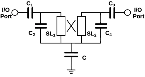
A common approach to producing finite transmission zeros is to form a feedback path by adding a coupling capacitor between I/O ports [5], [8]. However, the coupling capacitor is very small, so the filter’s response is very sensitive to the variation of the coupling capacitor. Besides, the finite transmission zeros produced from the feedback path can’t locate at the second harmonic of operating frequency, thus the filter can’t provide enough suppression at the second harmonics. This thesis presents a band-pass filter of serial-configuration with two finite transmission zeros, and demonstrates the filter using LTCC technology. The proposed filter is based on a conventional filter architecture with transmission zeros at DC and infinite frequency, and incorporates a capacitor C between the traditional filter and the ground, as shown in Fig. 2.1. The grounding capacitor provides a feedback path to the common band-pass filter and, as explained below, generate two finite transmission zeros at different sides of the pass-band. Section 2.1 describes the proposed filter’s operation and validates its configuration function using the filter network’s impedance matrix [13] together with graphical solutions [5], [6]. The 3-D layouts of two LTCC band-pass filters with the proposed schema are also illustrated. The filters were designed and simulated using a full-wave electromagnetic (EM) simulator. Finally, the measurement results of the two fabricated LTCC filters are presented. The experimental and simulation results were found to agree.
2.1 Theory and Design
The proposed filter schema in Fig. 2.1 can be regarded as two two-port networks connected in series, with the upper and lower parts shown in Fig. 2.2(a). The upper network (Network 1) can be a conventional band-pass filter with infinite transmission zero, such as a band-pass filter with an equal-ripple or maximally-flat response [13]. The filter schema chosen for this study is illustrated in Fig. 2.2(b). The lower network (Network 2) is simply a shunt capacitor C as illustrated in Fig. 2.2(c). In the upper network, C2 and the strip-line section SL1 form a resonator, as do C4 and the strip-line
SL2. The two resonators can generate two poles, supporting the filter’s pass-band. The
coupled strip-lines SL1 and SL2 couple the major portion of signal energy between the
I/O ports close to the center frequency. Capacitors C1 and C3 act as inverters matching
the resonators to the external impedance [13] and as DC-decoupling capacitors to block the DC signal at the front or back stage of the filter. As demonstrated below, this upper network behaves as a band-pass filter without finite transmission zeros if the grounding capacitor C is omitted. C C1 C3 C2 SL1 SL2 C4 I/O Port I/O Port C C1 C3 C2 SL1 SL2 C4 I/O Port I/O Port
The impedance matrix Z of the proposed filter configuration in Fig. 2.2(a) can easily be derived as the sum of the upper (ZU) and lower network (ZL) matrices, that is,
Z = Z
U+ Z
L.
(1)These impedance matrices assumed the filter to be lossless, and thus are purely imaginary, that is, Z = jX, where X denotes the corresponding reactance matrix. Notably, for the simple lower network shown in Fig. 2.2(c), the elements (ZL) of the
impedance matrix are the same and can be derived as
C
1
-
X
Z
L Lω
j
j
=
=
(2)Network theory relates the scattering parameter S21 (i.e., the transmission coefficient)
of the filter to the impedance matrix elements Zij, i, j = 1, 2, by the following formula
[13]:
Z
(Z
Z
)Z
(Z
Z
Z
Z
)
Z
2Z
S
21 12 22 11 0 22 11 2 0 21 0 21−
+
+
+
=
(3)where Z0 represents the characteristic impedance of the I/O ports, set to 50 Ω in this study.
The finite transmission zeros of the filter are located at the frequency ω where S21(ω) = 0,
or, from (3), Z21(ω) = 0. Restated, the frequency of the finite transmission zeros
Z
U21(
ω
)
=
-
Z
L21(
ω
)
(4) or C 1 ) ( XU21 ω =ω
(5) Network 1 ZU Network 2 ZL Port 1 Port 2 Network 1 ZU Network 2 ZL Port 1 Port 2 (a) C1 C3 C2 SL1 SL2 C4 I/O Port I/O Port C1 C3 C2 SL1 SL2 C4 I/O Port I/O Port (b) C I/O Port I/O Port C I/O Port I/O Port (c)Fig. 2.2 (a) Representation of the proposed filter with two serially-connected networks. (b) The upper network (Network 1). (c) The lower network (Network 2).
The transmission zeros can be located analytically by first considering the two coupled strip lines (SL1 and SL2) in Fig. 2.2(b) as two inductors L1 and L2 with mutual
inductance of M. Then, by correctly cascading the ABCD matrices of the input/output capacitor circuits and the inductor circuit, the ABCD matrix, and thus the Z matrix (ZU),
of the upper network can be derived as follows:
(
)
M M C L M C L M L L M C C j 1 ) ( Z 4 2 2 1 2 2 1 4 2 3 21 Uω
ω
ω
ω
+ ⎟ ⎠ ⎞ ⎜ ⎝ ⎛ + − − = . (6)Finally, substituting (6) into (5) generates a fourth-order polynomial equation of ω:
(
2)
2 1 2 2 4 1 0 2 1 4 2 4 ⎟+ = ⎠ ⎞ ⎜ ⎝ ⎛ + + − − M M C L M C L C M L L M C Cω
ω
, (7)whose two positive roots are the frequencies of the finite transmission zeros.
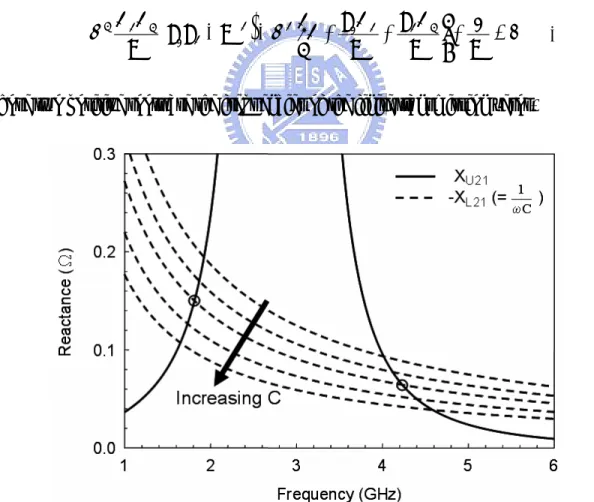
Fig. 2.3 Mutual reactance function XU21 of the upper network (network 1) and the
The characteristic equation (5) for transmission zeros can also be solved graphically. Figure 2.3 depicts the left-hand side (solid line) and right-hand side (dashed lines) of (5) as frequency functions. The mutual reactance function XU21(ω) of the upper network
in Fig. 2.2(b) was calculated with the circuit simulator Microwave Office [14], using a symmetrical geometry with C1 = C3 = 1.1 pF and C2 = C4 = 2.52 pF. The strip-lines SL1
and SL2 had identical dimensions, 3.1 mm × 0.1 mm (length × width), with a narrow
spacing of 0.1 mm to ensure sufficient mutual inductance. Figure 2.3 compares five reactance curves for the lower network with the grounding capacitance varying from 8.5 pF to 18 pF. In Fig. 2.3, the dashed lines denote grounding capacitances of C = 8.5 pF, 10 pF, 11.6 pF, 14 pF and 18pF. The finite transmission zeros are located where the solid line intersects with the dashed lines. The filter’s transmission zeros, which obey the relationship (5), correspond to the intersection points between the solid line and the dashed lines. Clearly each grounding capacitance has two intersection points, i.e., two finite transmission zeros. Additionally, the locations of the two transmission zeros expand outward as the grounding capacitance increases. The desired transmission zeros can be obtained for the band-pass filter by selecting appropriate grounding capacitance values.
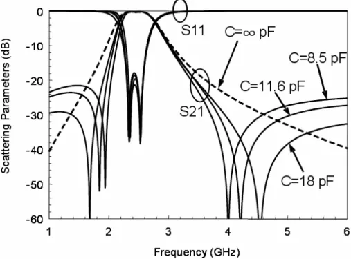
Figure 2.4 illustrates the computed return loss (S11) and insertion loss (S21) of the
entire band-pass filter of Fig. 2.1. The solid lines denote the results for three grounding capacitances (C = 8.5 pF, 11.6 pF and 18 pF), while the dashed lines represent those of the conventional filter structure (Fig. 2.2(b)), which is equivalent to the proposed filter with infinite grounding capacitance (C = ∞). The graph demonstrates that, changing the grounding capacitance does not alter the filter’s pass-band, which remains the same as that of the conventional filter. That is, connecting a grounding capacitor in series with a
conventional filter does not influence the insertion and return losses in the pass-band. This phenomenon was also noted in the filter with a feedback capacitor connecting the I/O ports [5]. Furthermore, Fig. 2.4 shows that each filter configuration with a grounding capacitor possesses two finite transmission zeros, one in the lower stop-band and the other in the higher stop-band. The frequency of the lower zero falls, while that of the higher zero rises, as the grounding capacitance increases. At the limit, when the capacitance is increased to infinity, the transmission zeros converge to a DC zero and an infinite zero, as in the conventional filter. Significantly, the transmission zeros are located precisely at the intersection points in Fig. 2.3 for each grounding capacitance.
Fig. 2.4 Scattering parameters (ideal responses) of the proposed band-pass filter with different grounding capacitances.
Equation (4) indicates that transmission zeros can be produced by serially connecting two networks with positive and negative reactance. The proposed filter has an inductive
upper network with positive reactance, and a capacitive lower network with negative reactance. The lower network is used to form a feedback so as to produce finite transmission zeros. If the upper network is capacitive, then the lower network should be inductive with positive reactance [6].
2.2 LTCC Layouts and EM Simulation
Based on the proposed filter schema, two band-pass filters with different pass-bands were designed and fabricated using the LTCC process. The first step is to adjust the filter’s component values with the circuit simulator to obtain the ideal frequency responses. Second, a multilayer LTCC structure is designed using the new component values, and simulated using the full-wave commercial package HFSS [15], which is a 3-D finite-element-based EM simulator. At this stage, the mutual coupling of the filter components in the compact multilayer structure would result in different simulation responses from those obtained initially. Therefore, the LTCC layout is finally fine-tuned to minimize the difference between the full-wave simulation results and the ideal results.
The first band-pass filter designed in this study is typically applied in Bluetooth or IEEE 802.11 b/g WLAN, which has a pass-band bandwidth of nearly 100 MHz centered at 2.44 GHz. Besides low insertion loss in the pass-band, the filter should also produce a high rejection at 1.8/1.9 GHz and at around 4.9 GHz to suppress the DCS 1800 interference signal and the second harmonic of the operating frequency. The filter has circuit component values with ideal frequency responses as described in Section II with the grounding capacitance C = 11.6 pF.
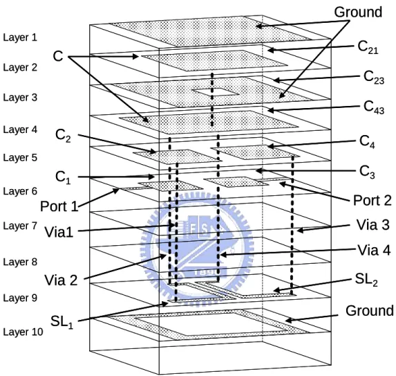
and shown in Fig. 2.5. The dielectric constant of LTCC substrate for each layer is 7.8 (at 2.5 GHz); the loss tangent is 0.004 (at 2.5 GHz). The first filter contained ten LTCC layers. The top six layers were 0.039 mm thick, and the others were 0.087 mm thick. The thickness of the metal plates (silver alloy) was 0.02 mm. Since the grounding capacitor had a large capacitance value of 11.6 pF, the top four layers were employed to realize its capacitance. Layer 1 and Layer 3 were ground layers, connected to each other by the side-pads (not depicted in the diagram) on the longer edges of the LTCC substrate. The metal plate on Layer 2 generated two capacitors C21and C23 to grounds (Layer 1 and
Layer 3), respectively. Additionally, Layer 4 produced a capacitor C43 to the third-layer
ground. After equalizing the potentials on the two metal plates by a via, the three capacitors (C21, C23 and C43) were connected in parallel with C = C21 + C23 + C43, thus
realizing the large grounding capacitor.
The capacitors C1 and C3, which were connected in series to Ports 1 and 2 (I/O ports),
respectively, were generated by the metal plates on Layer 6 and Layer 5. The capacitors C2 and C4 in the two resonators of the filter were produced by the plates on Layer 5 and
Layer 4. The strip-line SL1 between C1 and C was connected to C1 by Via 1 and
connected to C by Via 2. Notably, these two vias would contribute a small inductance to SL1. Similarly, SL2 was connected to C3 by Via 3 and connected to C by Via 4. The
strip-lines were located on Layer 9 with 0.1 mm spacing, considering the limitation of distance between two adjacent lines in fabrication. The required mutual inductance could be obtained using an appropriate coupling length. Significantly, the mutual inductance was formed by edge-coupled, instead of broadside-coupled, strip-lines. This coplanar layout would reduce the inaccuracy in LTCC fabrication, because the error
probability of metal offset in edge coupling is much smaller than that in broadside coupling. Furthermore, the edge-coupled strip-lines maintained the symmetry of the 3-D layout, and thus the symmetry of the filter functions.
Ground
C
C
2C
1SL
1C
3C
4SL
2Ground
Port 1
Port 2
Layer 1 Layer 2 Layer 3 Layer 4 Layer 5 Layer 6 Layer 7 Layer 8 Layer 9 Layer 10Via1
Via 2
Via 3
Via 4
C
21C
23C
43Ground
C
C
2C
1SL
1C
3C
4SL
2Ground
Port 1
Port 2
Layer 1 Layer 2 Layer 3 Layer 4 Layer 5 Layer 6 Layer 7 Layer 8 Layer 9 Layer 10Via1
Via 2
Via 3
Via 4
C
21C
23C
43Fig. 2.5 3-D LTCC layout of the 2.4-GHz band-pass filter.
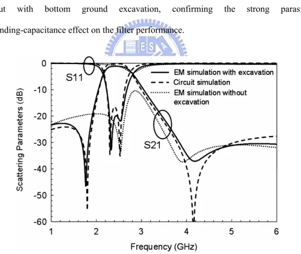
The bottom layer (Layer 10) was a ground with the central part excavated in order to avoid the large parasitic grounding-capacitance effect between the two strip-lines and the ground. These three ground layers (Layer 1, Layer 3, and Layer 10) were connected by the side-pads on the two longer edges of the LTCC substrate, and the I/O ports are on the shorter edges of the LTCC. The total size of the LTCC band-pass filter was 2.5 × 2.0 ×
0.82 mm3. Figure 2.6 shows the full-wave EM simulation results for the 3-D LTCC layout, as compared to the ideal responses computed by the circuit simulator. The EM simulation results were found to agree with the ideal ones except for higher insertion loss in the pass-band resulting from the conductor and dielectric losses considered in the EM simulation. These results demonstrate that the 3-D configuration is a good band-pass filter with low in-band insertion loss and high out-band rejection (larger than 30 dB) at 1.8/1.9 GHz and the second harmonic frequency (around 4.9 GHz). Figure 2.6 also illustrates the EM simulation results for the LTCC layout without bottom ground excavation. These results differ significantly from the EM simulation results for the layout with bottom ground excavation, confirming the strong parasitic grounding-capacitance effect on the filter performance.
Fig. 2.6 EM simulated scattering parameters of the 2.4-GHz band-pass filter with and without excavated bottom ground plane.
The second band-pass filter was designed with a bandwidth larger than 0.9 GHz centered at the frequency of 4.8 GHz. Using the proposed filter schema in Fig. 2.1, an ideal band-pass filter response was obtained with C1 = C3 = 1 pF, C2 = C4 = 1.96 pF, C =
4.2 pF. The dimensions (length × width) of SL1 and SL2 were both 1.05 mm × 0.15 mm.
The spacing between strip-lines was set to 0.15 mm.
C
C
2C
1SL
1Ground
C
3C
4SL
2Ground
Port 1
Port 2
Layer 1 Layer 2 Layer 3 Layer 4 Layer 5 Layer 6 Layer 7 Layer 8 Layer 9 Layer 10 Layer 11C
C
2C
1SL
1Ground
C
3C
4SL
2Ground
Port 1
Port 2
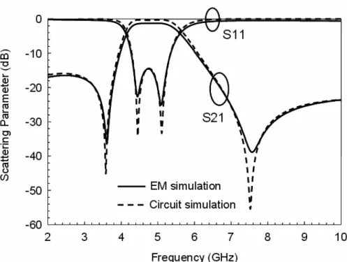
Layer 1 Layer 2 Layer 3 Layer 4 Layer 5 Layer 6 Layer 7 Layer 8 Layer 9 Layer 10 Layer 11Fig. 2.8 Scattering parameters of the 4.8-GHz band-pass filter calculated by EM simulator and circuit simulator.
In this case, all components were smaller in this band-pass filter than those in the 2.4-GHz band-pass filter. Therefore, this filter was realized in a smaller size of 2.0 × 1.2 × 0.88 mm3, with the 3-D LTCC layout revealed in Fig. 2.7. The LTCC had eleven
layers; the top seven layers were 0.039 mm thick, while the other layers were 0.087 mm thick. This filter, being smaller than the previous filter, constructed the grounding capacitor C using only the top two layers. Moreover, three layers were employed to construct C1 and C3, from Layer 3 to Layer 5, with connecting the plates on Layer 3 to
those on Layer 5 by vias, forming two vertical interdigital capacitors. The strip-lines SL1 and SL2 on Layer 7 were respectively connected to C1 and C3 by vias, and to each
other at a buffer pad on Layer 6. The buffer pad was connected to the grounding capacitor C through a via from Layers 6 to 2. The buffer pad reduced the total number of required
vias, thus pushing cost down and increasing the fabrication yield. Notably, the strip-lines were in parallel with the capacitors C2 and C4 formed between Layer 3 and
Layer 2. Additionally, the bottom ground did not need to be excavated since the strip-lines’ layer was far from the bottom ground. Figure 2.8 compares the EM simulation results for the 3-D layout with the ideal responses calculated by the circuit simulator. These results agree with each other quite well.
2.3 Experimental Results
After the analysis and EM simulation, the designed filters were fabricated using the Dupont 951 LTCC process with dielectric constant of 7.8 (at 2.5 GHz), loss tangent of 0.004 (at 2.5 GHz) and thickness of the silver alloy of 0.02 mm. The commonly used printed-circuit board FR4 with dielectric constant of 4.4, loss tangent of 0.02, and thickness of 0.4 mm was applied as the test board to measure the performance of the fabricated LTCC filters.
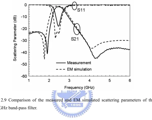
Figure 2.9 shows the measured results for the 2.4-GHz band-pass filter, together with the EM simulation results. The two transmission zeros of the measured response occurred at 1.9 GHz and 4.3 GHz, which are 100 MHz higher than in the simulation. Significantly, the zero at the high-skirt side on the measured result, which is much deeper than that of the simulation, can provide a signal suppression (1/S21) of 45 dB. Moreover,
in the measured results, the second harmonic of 2.4 GHz signal could be suppressed to −38 dB, and the suppression during 3.7 GHz to 6 GHz was higher than 30 dB. The zero on the low-skirt side provided suppressions of 41 dB at 1.916 GHz, 38 dB at 1.9 GHz, and 27 dB at 1.8 GHz. The pass-band insertion loss from 2.4 GHz to 2.483 GHz was
better than 1.93 dB, with a minimum value of 1.7 dB at 2.48 GHz. The measured response agrees well with that of the EM simulation.
Fig. 2.9 Comparison of the measured and EM simulated scattering parameters of the 2.4-GHz band-pass filter.
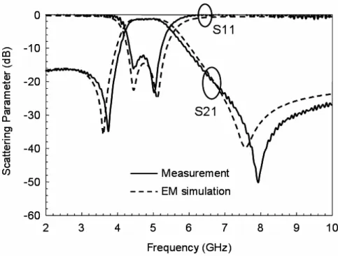
Figure 2.10 compares the measured and EM simulated results for the 4.8-GHz band-pass filter. The measured response agrees well with the EM simulation response except that the two finite transmission zeros shifted slightly to higher frequencies in the measured response. In the measured results, the 1.5-dB insertion-loss bandwidth extended from 4.42 GHz to 5.16 GHz, with a minimum value of 1.16 dB at 5 GHz. The suppression was 35 dB at the lower zero (3.75 GHz) and 50 dB at the higher zero (7.96 GHz). The 4.8-GHz band-pass filter had a larger pass-band fractional bandwidth, but a worse out-band rejection at the lower side of the pass-band, compared to the 2.4-GHz band-pass filter. This difference was found because the ratios of the zero location to the
band edge for two designs are different. The closer the zero is to the band edge, the less the ultimate rejection will be got. In Fig. 2.9, the ratio of the lower zero to the lower band edge in the measured results is 2.4/1.916=1.2526, while in the 4.8-GHz band-pass filter (Fig. 2.10) the ratio is 4.42/3.75=1.1786. Consequently, the 2.4-GHz filter has more ultimate rejection at the low-skirt side owing to a farther zero than that of the 4.8-GHz filter.Figure 2.11 presents a photograph of the two fabricated LTCC filters.
Fig. 2.10 Comparison of the measured and EM simulated scattering parameters of the 4.8-GHz band-pass filter.
Fig. 2.11 Photograph of the two fabricated LTCC filters. The photograph on the left shows the 2.4-GHz BPF, and the other shows the 4.8-GHz BPF.
Chapter 3 RF Front-End Antenna Switch
Module
To miniaturize components, the System-on-Package techniques become more and more important in recent years. By properly designing on multi-layer substrate such as LTCC, we can integrate active components (such as power amplifiers, low-noise amplifiers, and T/R or diversity switches) and buried passive components (such as low-pass filters, band-pass filters, diplexers, and matching circuits) into a package. As shown in Fig. 3.1, the active components (bare dies are used usually) can be mounted on the top surface of the substrate, and the passive components are buried in the multi-layer substrate. The bond wire is thus necessary for the connection between bare dies and buried circuits. Because the bond wire is similar to the inductor, we have to take the effect of bond wire into account [19]-[21], in order to avoid the bond wire affecting the input impedance of the buried circuits. However, it is also workable to utilize the bond wire for compensation on the input impedance matching. In this chapter, a RF front-end antenna switch module is proposed. We consider the effect of the bond wire, and then design a band-pass filter and a low-pass filter that can incorporate the bond wire. Both the two filters are suitable for LTCC module integration. In addition, we encounter some problems while integrating this module, and the solutions to overcome the integration problems will also be presented.
Evaluation Board
Bare Die
Bond wire
LTCC Substrate
Evaluation Board
Bare Die
Bond wire
LTCC Substrate
Fig. 3.1 Side view of the bond wires connecting the bare die and buried circuits.
3.1 Block Diagram of Antenna Switch Module
The proposed RF front-end antenna switch module, which is applied in IEEE 802.11a WLAN (operating frequencies are from 4.9 to 5.85 GHz), consists of an embedded antenna, a band-pass filter, a low-pass filter, and a T/R Switch. The block diagram of the antenna switch module is shown in Fig. 3.2. The two filters and the antenna are buried in the LTCC substrate, while the T/R switch (bare die is used) is mounted on the top surface of the LTCC substrate. The interconnection between the switch and the buried circuits is established by bond wires. The transmit path contains a low-pass filter, a T/R switch, and an antenna; while the receive path contains an antenna, a T/R switch, and a band-pass filter. On the transmit path, the low-pass filter has not only to possess low insertion loss at pass band, but also to provide high suppression on the second and third harmonics of operating frequency. The band-pass filter used on the receive path must has low insertion loss at pass band, and must provide enough suppression to filter the second harmonic signals of operating frequencies and to suppress
GHz), GSM (0.9 GHz), DCS (1.8 GHz), and PCS (1.9 GHz).
The T/R switch is used to switch the antenna to connect with the band-pass filter or with the low-pass filter for receiving or transmitting signals, respectively. Thus the requirement for the T/R switch is low insertion loss at operating band and high rejection between through and isolation ports. As to the antenna, good return loss performance and omni-directional radiation patterns are required.
Rx
5GHz
Antenna
T/R
Diversity
Switch
5GHz
BPF
5GHz
LPF
Tx Rx5GHz
Antenna
T/R
Diversity
Switch
5GHz
BPF
5GHz
LPF
TxFig. 3.2 Block diagram of the RF front-end antenna switch module.
3.2 Band-pass Filter Design
3.2.1 Band-pass Filter Configuration
Different from the traditional filter structures [5], [7], [22] that use capacitors to be impedance inverters; the proposed filter utilizes an inductor to do the same work. The
inductor can be implemented by the external bond wire rather than internal buried circuits. To show the effect of a bond wire, an example shown in Fig. 3.3 is illustrated. Fig. 3.3(a) shows a commonly used third-order band-pass filter, which uses two capacitors as impedance inverter at I/O ports, the full-wave simulated result is shown in Fig. 3.3(c) (dash lines). After connecting an inductor (0.82 nH) as bond wire (shown in Fig. 3.3(b)), the response of pass-band insertion loss (S21) becomes uneven, and the input matching
becomes bad (S11 is less than 10 dB), the result are illustrated in Fig. 3.3(c) (solid lines).
The schema of the proposed band-pass filter for this module integration is shown in Fig. 3.4. It is a third-order filter with two series LC and one parallel LC resonators. The two series LC resonators can provide the finite transmission zeros at lower frequencies, and the parallel LC resonator can generate a pole to support the pass band. The two striplines SL1 and SL2 are open-end stubs, which are quarter-wavelength resonators
providing the transmission zeros at higher frequencies (about at the second harmonics of operating frequencies). The capacitors C1 and C2 are used to control the coupling between
LC resonators and act as DC-decoupling capacitors to block the DC signal in the front or back stage of the filter. The stripline SL6 acts as an impedance inverter matching the
resonators to the external impedance, so as the inductor L. Notably, the inductor L is not buried in the LTCC substrate, but is implemented utilizing the external bond wire which is used to connect the band-pass filter and the top-surface bare die (the T/R switch).
I/O Port C1 I/O Port C2 C5 C3 C4 L1 C6 L2 L3 C7 I/O Port C1 I/O Port C2 C5 C3 C4 L1 C6 L2 L3 C7 (a) Bond wire I/O Port C1 I/O Port C2 C5 C3 C4 L1 C6 L2 L3 C7 L Bond wire I/O Port C1 I/O Port C2 C5 C3 C4 L1 C6 L2 L3 C7 L (b) 1 2 3 4 5 6 7 8 9 10 11 12 Frequency (GHz) -50 -40 -30 -20 -10 0 S-Pa ra me te rs ( d B)
With bond wire Without bond wire
S21 S11 1 2 3 4 5 6 7 8 9 10 11 12 Frequency (GHz) -50 -40 -30 -20 -10 0 S-Pa ra me te rs ( d B)
With bond wire Without bond wire With bond wire Without bond wire
S21 S11
(c)
Fig. 3.3 (a) Schema of commonly used filter with capacitors as impedance inverter (b) Schema with bond wire (c) Full-wave simulated results of (a) and (b).
I/O Port C1 SL6 I/O Port C2 C5 C3 C4 SL3 SL4 SL1 SL2 SL5 L I/O Port C1 SL6 I/O Port C2 C5 C3 C4 SL3 SL4 SL1 SL2 SL5 L
Fig. 3.4 Schema of the proposed band-pass filter for module integration.
3.2.2 EM Simulation
In this section, the first step is to simulate the effect of a bond wire using a full-wave electromagnetic (EM) commercial package HFSS, and then we take the results (scattering parameters) to replace the inductor L in Fig. 3.4. The 3-D simulation layout of the bond wire is shown in Fig. 3.5, and the simulated results of the bond wire and comparison with an inductor of 0.82 nH are illustrated in Fig. 3.6. From Fig. 3.6, it is obvious that the bond wire is similar to an inductor of 0.82 nH. Then, the second step is to adjust the rest of the component values of the filter by a circuit simulator to obtain the ideal frequency responses. The third step is to implement the filter in a real LTCC multi-layer substrate using the EM simulator. Finally, the 3-D layout (as shown in Fig. 3.9) is fine-tuned to make the EM simulated results as close to the ideal responses as possible. The full-wave simulated results without bond wire is shown in Fig. 3.7 (dash lines), and the ones with bond wire is shown in Fig. 3.8 (dash lines). From these two figures, two differences are
obvious. One is the pass-band responses and the other is the second harmonic suppressions. The pass band in Fig. 3.8 is more flat than that in Fig. 3.7, besides, two poles appear in Fig. 3.8 while one in Fig. 3.7. The harmonic suppressions in Fig. 3.8 are higher than that in Fig. 3.7. The two phenomena are both due to the bond wire, which compensates the input impedance matching of the pass band and provides more suppression at higher frequencies.
LTCC substrate Evaluation Board Bare Die Bond wire LTCC substrate Evaluation Board Bare Die Bond wire
Fig. 3.5 Side view of the bond wire’s layout.
Fig. 3.7 EM simulated and measured results without a bond wire.
(a) Oblique view
(b) Side view
(c) Top view Fig. 3.9 3-D layouts of the band-pass filter.
3.2.3 Experimental Results
After the analysis and EM simulation, the designed filter was fabricated using the CT2000 LTCC process with the dielectric constant of 9.1 (at 2.5 GHz), the loss tangent of 0.002 (at 2.5 GHz), and the thickness of the silver alloy of 0.012 mm. The commonly used printed-circuit board FR4 with the dielectric constant of 4.4, the loss tangent of 0.02, and the thickness of 0.4 mm was applied as the evaluation board to measure the performance of the fabricated LTCC filter. This filter was measured by probes which were connected to the network analyzer HP8510C. The first filter was measured without the bond wire, and its result is shown in Fig. 3.7. Note that the pass-band response was not flat due to bad input matching. After bonding a wire to the I/O port of the filter, the measured result demonstrated in Fig. 3.8 shows that the pass-band response was much better than that in Fig. 3.7, and the input matching became wider. Notably, there was only a pole in Fig. 3.7, whereas two poles appeared in Fig. 3.8. Consequently, it is so important that we have to consider the effect of bond wires before integrating active components and LTCC buried circuits into a package. In Fig. 3.8, although the measured results showed a bit shift to lower frequencies due to process inaccuracy, the two results were found to agree well with each other. The measured insertion losses from 4.43 to 6.02 GHz were less than 1.4 dB, with a minimum value of 0.8 dB at 5.55 GHz. Moreover, with the transmission zero providing a suppression of 47 dB at 10.7 GHz, the second harmonics could be suppressed more than 25 dB. In addition, the suppression during 1 to 2.5 GHz was higher than 45 dB.
3.3 Low-pass Filter Design
3.3.1
Low-pass Filter Configuration
The commonly used low-pass filter is shown in Fig. 3.10(a), and this is a fifth order low-pass filter. After adding an inductor (0.82 nH) to this conventional low-pass filter (shown in Fig. 3.10(b)), the return loss becomes bad and the pass-band response becomes uneven, thus the pass-band insertion loss is too much. The simulation results are illustrated in Fig. 3.10(c), the dash lines and the solid lines denote the scattering parameters of Fig. 3.10(a) and Fig. 3.10(b), respectively. Consequently, it is obvious to see how much the bond wire will affect the input impedance matching. In order to solve this problem, we have to design other structures of low-pass filter that can utilize the bond wire to compensate the input matching, as discussed in Section 3.2.
The schema of the proposed low-pass filter incorporating the bond wire effect for this module integration is shown in Fig. 3.11. Compared with the filter in Fig. 3.10(b), the proposed low-pass filter has only 6 elements rather than 8 elements. Moreover, the inductor can be implemented by utilizing external bond wire which is used to connect the low-pass filter and the top-surface bare dies (the T/R switch). In Fig. 3.11, the resonator formed by a capacitor and a stripline can provide two finite transmission zeros at the second and the third harmonics of the operating frequencies. By changing the length of the stripline or the value of the capacitor in the resonator, we can control the frequency locations of the two finite transmission zeros. The proposed low-pass filter is simpler and has better performance than those of the conventional low-pass filter. The ideal simulation results are shown in Fig. 3.12, and it’s obvious to see that this low-pass filter has low insertion loss at pass band and high suppression at the 2nd and 3rd harmonics.
(a)
(b)
(c)
Fig. 3.10 (a) Schema of conventionally used low-pass filter (b) Schema with a bond wire (c) Simulation results of (a) and (b).
Fig. 3.11 Schema of the proposed low-pass filter for module integration.
3.3.2
EM Simulation
In this section, the design flow is as the same as Section 3.2.2. We use the EM simulator (HFSS) to draw the 3-D layouts of the low-pass filter and to simulate the scattering parameters. The 3-D layouts including oblique view, side view, and top view, are shown in Fig. 3.13. Because this filter is simple and has only 5 buried elements, we use only 3 layers for this layout. In order to avoid the fabrication error affecting the filter too much, we use thick layer for this layout to reduce the sensitivity. The interdigital capacitor will shift a bit due to the inaccuracy of fabrication process, thus may change the value of the capacitor. As a result, we can enlarge the distance between the two parallel plates and make one of the two parallel plates larger than the other, and the sensitivity to the fabrication error can be reduced. On the contrary, once we enlarge the distance between the two parallel plates, the area of the two plates also has to be increased to remain the value of demand. Consequently, that is a compromise among size, cost, and performance. Fig. 3.14 shows the EM simulation results of the low-pass filter. From Fig. 3.14, the insertion loss at pass band is less than -0.44 dB, and the suppression at the second and third harmonics are higher than 30 dB. Significantly, the finite transmission zero at 10.55 GHz can provide a suppression more than 60 dB.
(a) Oblique view
(b) Side view
(c) Top view Fig. 3.13 3-D layouts of the low-pass filter.
Fig. 3.14 EM simulation results of the low-pass filter.
3.3.3
Experimental Results
After the analysis and EM simulation, the designed low-pass filter was fabricated using the CT2000 LTCC process with the dielectric constant of 9.1 (at 2.5 GHz), the loss tangent of 0.002 (at 2.5 GHz), and the thickness of the silver alloy of 0.012 mm. The commonly used printed-circuit board FR4 with the dielectric constant of 4.4, the loss tangent of 0.02, and the thickness of 0.4 mm was applied as the evaluation board to measure the performance of the fabricated LTCC filter. This filter was measured by probes which were connected to the network analyzer HP8510C. The first filter was measured without the bond wire, and its result is shown in Fig. 3.15. Note that the pass-band response was not flat due to bad input matching. The insertion loss at pass band are a little higher, the losses at 4.9 and 5.85 GHz are -0.41 and -0.733 dB, respectively. The scattering parameter S21 at higher frequencies about third harmonics
can not provide enough suppression, and it likes that the S21 will ascend as the frequency
increases. After bonding a wire to the I/O port of the filter, the measured result demonstrated in Fig. 3.16 shows that the pass-band response is much better than that in Fig. 3.15, and the input matching became deeper. Consequently, one can observe that we have to consider the effect of bond wires before integrating active components and LTCC buried circuits into a package. In Fig. 3.16, although the measured results showed a bit shift to higher frequencies due to fabrication process inaccuracy, the two results were found to agree well with each other. The measured insertion losses from 4.9 to 5.85 GHz were less than 0.34 dB, with a minimum value of 0.235 dB at 4.9 GHz. Moreover, with the transmission zero providing a suppression of 54.4 dB at 10.76 GHz, the second harmonics could be suppressed more than 26 dB. In addition, the suppression at the third harmonics was higher than 25 dB.
Fig. 3.16 Measured results of the low-pass filter with a bond wire.
3.4 Embedded Antenna Design
3.4.1
Antenna Structure
In this section, we design an embedded antenna in the LTCC multilayer substrate. This antenna is required to have input impedance near 50Ω for good return loss (S11) and
to possess proper antenna gains (with peak gain larger than 0 dBi), and the radiation patterns are must be as omni-directional as possible for operating frequencies. The antenna designed for this module is based on the inverted-F antenna. The structure of the inverted-F antenna is shown in Fig. 3.17. L1 represents the length of the end which is
open-circuited. We can use an equivalent transmission-line model (as shown in Fig. 3.18) to demonstrate the inverted-F antenna. The resonant frequency (or the total length of the radiating element) can be determined from this equivalent model. As the length of (L1+L2)
is around the quarter wavelength of the resonant frequency, the input reactance will vanish due to the resonance of the inductor-like short-circuited line and the capacitor-like open-circuited line. The input admittance of the feeding point is as follows:
0 2 0 1 0 0 2 0 2 0 2 0 0 2 2 2 2 0 0 0 0 0 0 0 0 2 2 0 tan cot tan tan cot ( tan ) tan sin
: the radiation conductance : admittan in in G jY Y jY Y Y jG G jY jY Y T Y jG jY T Y GT Y G jY T Y jGT G Y Y jGT Y G Y G Y 2 β β β β β β β β + = − + + + = − + = + − + + + = + ∴ + ≈ = ∵ 1 2
ce of the transmission line : length of the short-circuited end
: length of the open-circuited end
For compactness, the antenna switch module is designed on a printed circuit board (PCB) as the evaluation board, which has a size of 55 mm × 20 mm, and this is a size of commonly used USB dongle. The material of the PCB is FR4, which has a dielectric constant of 4.4, a loss tangent of 0.02, and the thickness of the PCB substrate is 0.4 mm. The ground size of the substrate is set as (50 mm × 20 mm + 5 mm × 4 mm), and the geometry of the PCB is shown in Fig. 3.19(a). Moreover, the LTCC substrate’s size is only 6.2 mm × 5.4 mm. The geometry of the embedded inverted-F antenna is shown in
Fig. 3.19(b). In order to reduce the antenna size of the inverted-F antenna, the open-circuited end is bended downward to fit the LTCC substrate’s size. Therefore, the antenna area in the LTCC substrate is merely 5.4 mm × 4.0 mm, and the rest area is for the band-pass and low-pass filters. Dupont 951 process is used for this antenna switch module fabrication. The material of the LTCC substrate has a dielectric constant of 7.8, a loss tangent of 0.002, and the thickness of the LTCC substrate is 0.98 mm. In addition, the conductivity of the alloy in the LTCC substrate is 3.0 × 10⁷ (S/m).
Feeding point
Ground Feeding point
Ground
Fig. 3.17 Structure of the inverted-F antenna.
(a)
(b)
3.4.2
EM Simulation
The commercial EM simulator HFSS is used to simulate the 3-D LTCC embedded antenna. From Fig. 3.20, we can see the drawing of the inverted-F antenna. Different from Fig. 3.17, the open-circuited end is bended in this design such that we can miniaturize the module size as we can as possible. Notably, the short-circuited end is implemented using a grounding via, which connects the short-circuited end and the ground inside the LTCC substrate, and then the LTCC grounding is made by connecting with the FR4’s ground by several vias. In addition, the open-circuited end is designed on the top surface of the LTCC substrate rather than in the buried layer of the substrate. This is because we can change the resonant frequency by modifying the length outside the LTCC substrate if the resonant frequency is shifted due to process inaccuracy. As a consequence, the embedded inverted-F antenna occupies only two layers. The EM simulated result (S11) is presented in Fig. 21. The bandwidth of return loss larger than 10
dB is from 4.81 to 5.96 GHz. And the bandwidth is enough for IEEE 802.11a (4.9~5.85 GHz) WLAN applications. Besides, the simulated far field’s radiation patterns in principal planes for 5.3 GHz are shown in Fig. 22. The radiation patterns are quite omni-directional in the X-Z and Y-Z plane, while the radiation in the X-Y plane is acceptable for our demand. The peak gains in the X-Z plane, Y-Z plane, and X-Y plane are 2.72 dBi, 0.34 dBi, and 1.95 dBi, respectively, as the average gains in the X-Z plane, Y-Z plane, and X-Y plane are 1.18 dBi, -0.87 dBi, and -1.26 dBi, respectively. Table 3.1 summarizes the EM simulated radiation peak and average gains of E-Total field for each principal plane of the miniaturized embedded inverted-F antenna.
(a) Oblique view
(b) Oblique view
Grounding vias Grounding vias
(b) Grounding vias between PCB and LTCC substrate Fig. 3.20 3-D layouts of the embedded inverted-F antenna.
Fig. 3.21 EM simulated return loss (S11) of the embedded inverted-F antenna. -35 -30 -25 -20 -15 -10 -5 0 5 -35 -30 -25 -20 -15 -10 -5 0 5 -35 -30 -25 -20 -15 -10 -5 0 5 -35 -30 -25 -20 -15 -10 -5 0 5 0 30 60 90 120 150 180 210 240 270 300 330 E-phi E-theta x y z x y z (a) X-Z plane
-35 -30 -25 -20 -15 -10 -5 0 5 -35 -30 -25 -20 -15 -10 -5 0 5 -35 -30 -25 -20 -15 -10 -5 0 5 -35 -30 -25 -20 -15 -10 -5 0 5 0 30 60 90 120 150 180 210 240 270 300 330 E-phi E-theta x y z x y z (b) Y-Z plane -35 -30 -25 -20 -15 -10 -5 0 5 -35 -30 -25 -20 -15 -10 -5 0 5 -35 -30 -25 -20 -15 -10 -5 0 5 -35 -30 -25 -20 -15 -10 -5 0 5 0 30 60 90 120 150 180 210 240 270 300 330 E-phi E-theta x y z x y z (c) X-Y plane
Fig. 3.22 EM simulated radiation patterns at 5.3 GHz in three principal planes for the embedded inverted-F antenna.
E-Total X-Z plane Y-Z plane X-Y plane Peak Gain 2.72 dBi 0.34 dBi 1.95 dBi Average Gain 1.18 dBi -0.87 dBi -1.26 dBi
Table 3.1 Peak and average gains of the EM simulated radiation patterns (E-Total field) at 5.2 GHz for the embedded inverted-F antenna.
3.4.3
Experimental Results
Fig. 3.23 shows the measured return loss of the inverted-F antenna. The measured 10-dB bandwidth of return loss is from 4.702 to 6.229 GHz, with a maximum value of 43 dB at 5.7 GHz. Compared with the EM simulated result, the measured result has wider 10-dB bandwidth. Thus the designed inverted-F antenna can satisfy the bandwidth requirement of IEEE 802.11a (4.9~5.85 GHz). In addition, the measured radiation patterns are presented in Fig. 24 for 4.9, 5.1, 5.3, 5.5, and 5.8 GHz. The total radiation patterns in the three principal planes are quite omni-directional for all the frequencies. The measured results agree quite well with the EM simulated ones. A peak gain of 1.5 dBi and average gain of -1.4 dBi are obtained with respect to 5.8 GHz in the X-Z plane, whereas a peak gain of 0.5 dBi and average gain of -1.22 dBi are gotten with respect to 4.9 GHz. Besides, in the Y-Z plane, a peak gain of 0.08 dBi and average gain of -6.71 dBi are obtained with respect to 5.3 GHz, whereas a peak gain of -0.64 dBi and average gain of -7.43 dBi are gotten with respect to 4.9 GHz. Furthermore, in the X-Y plane, a peak gain of 1.16 dBi and average gain of -2.56 dBi are obtained with respect to 4.9 GHz, whereas a peak gain of 0 dBi and average gain of -3.23 dBi are gotten with respect to 5.3 GHz. The measured radiation gains at each frequency for each principal plane are summarized in Table 3.2.
Fig. 3.23 Measured result (S11) of the embedded inverted-F antenna. x y z x y z (a) X-Z plane
x y z x y z (b) Y-Z plane x y z x y z (c) X-Y plane
Fig. 3.24 Measured radiation patterns in the three principal planes for the embedded inverted-F antenna.
Frequency Electric Field Direction Principal Plane and Maximum Gain Average Gain 4.9 GHz X-Z E-phi 0.50 -1.22 4.9 GHz X-Z E-theta -9.48 -17.10 4.9 GHz Y-Z E-phi -2.53 -7.46 4.9 GHz Y-Z E-theta -0.64 -7.43 4.9 GHz X-Y E-phi 1.16 -2.56 4.9 GHz X-Y E-theta -13.19 -20.71 5.1 GHz X-Z E-phi 0.59 -1.08 5.1 GHz X-Z E-theta -5.17 -14.07 5.1 GHz Y-Z E-phi -2.96 -7.70 5.1 GHz Y-Z E-theta 0.02 -6.67 5.1 GHz X-Y E-phi 0.84 -3.00 5.1 GHz X-Y E-theta -12.74 -19.57 5.3 GHz X-Z E-phi 0.75 -1.72 5.3 GHz X-Z E-theta -6.51 -13.92 5.3 GHz Y-Z E-phi -3.98 -8.20 5.3 GHz Y-Z E-theta 0.08 -6.71 5.3 GHz X-Y E-phi 0.01 -3.23 5.3 GHz X-Y E-theta -14.37 -20.36 5.8 GHz X-Z E-phi 1.50 -1.41 5.8 GHz X-Z E-theta -4.84 -14.16 5.8 GHz Y-Z E-phi -3.60 -8.89 5.8 GHz Y-Z E-theta -0.33 -7.46 5.8 GHz X-Y E-phi 1.00 -3.20 5.8 GHz X-Y E-theta -11.45 -17.14 (Unit: dBi) Table 3.2 Measured radiation gains at each frequency in each principal plane for the embedded inverted-F antenna.
3.5 DPDT Switch Verification
In this section, we verified the GaAs MMIC DPDT switch. Because we have to miniaturize the size of the whole module, the bare die is used for the module integration. The size of the switch bare die is 0.99 mm × 0.93 mm. Fig 3.25 shows the outline drawing of the bare die. To verify the DPDT switch, we mounted the bare die on the top surface of a LTCC substrate, and then the bare die was measured by probes which were connected with the network analyzer HP8510C. The measurement photograph is shown in Fig. 3.26. Although there were 3 probes in this photograph, only two of them worked and the other was terminated. This was because that the network analyzer HP8510C has only two ports for measurement. The operating frequencies are from 4.9 to 5.85 GHz. The measured results including insertion losses and isolations are all shown in Fig. 3.27. The insertion losses and isolation between Ant 1 and TX/RX are around 1 dB and more than 25 dB, respectively.
Ant 1
TX
RX
Gnd
Gnd
Vc1
Vc2
Ant 2
Gnd
Ant 1
TX
RX
Gnd
Gnd
Vc1
Vc2
Ant 2
Gnd
Fig. 3.26 Photograph of the bare die measured by probes.
(b) Through between Ant 1 and RX
(d) Isolation between Ant 1 and RX.
(e) Isolation between Ant 1 and TX/RX while all DC controls are OFF. Fig. 3.27 Measured results including insertion losses and isolations of the switch.
3.6 Module Integration
After the analysis and simulation of each single buried component in the module, the next step is to integrate these buried circuits and the embedded antenna into a package and to simulate the coupling effects and isolations among them. Because the simulation time of the whole antenna module is very long, we pre-simulate each buried components for saving simulation time, and then we integrate all the finished-simulated components into a package and fine tune the whole-module simulation. The size of this antenna switch module is merely 6.2 mm × 5.4 mm × 0.98 mm. There are 14 layers used in this LTCC substrate, which contains 7 thin layers and 7 thick layers. The thickness of each thin layer is 0.04 mm, while that of each thick layer is 0.09 mm. Besides, the thickness of each metal plate (silver alloy) is 0.006 mm. The first layer is the top-surface layer on the substrate, and the second layer is under the top layer, and so on. Notable, the second and the fourteenth layer are ground layer in order to shield other electromagnetic interference.
In this stage, we have to take the DC wiring for the switch into account, so the surface wiring has to be designed first. Fig. 3.28 shows the surface wiring and layout on the top surface of the LTCC substrate. Fig. 3.28(a) shows the top surface with transparent LTCC substrate, whereas Fig. 3.28(b) notes the name of each pad with opaque LTCC substrate, and Fig. 3.28(c) presents the connection between the DPDT switch and pads, which includes 2 DC control signals, 4 grounds, 2 antennas, 1 TX path, and 1 RX path. In addition, the external matching circuits are also considered in this stage. It is clear that from Fig. 3.28(b) and (c), the π-matching circuit is applied on the pad named Ant. Feed, and the surface mount device (SMD) between Pad 2 and Pad3 is the DC-blocking capacitor. Significantly, Pad 1 and Pad 2 are connected through buried 50Ω transmission
line in the LTCC substrate. This is because that we have to avoid the surface mount solder paste, which is used for mounting the SMD components, flowing from Pad 2 to Pad 1 and then affecting the mounting of the bond wire connected from Pad1 to the switch. Vc1 Vc2 Gnd Gnd Gnd Gnd TX RX Gnd Ant. Feed Ext. Ant. Gnd 1 2 3 Vc1 Vc2 Gnd Gnd Gnd Gnd TX RX Gnd Ant. Feed Ext. Ant. Gnd 1 2 3
(a) With transparent LTCC substrate (b) With opaque LTCC substrate
SMD SMD SMD SMD Switch Gnd SMD SMD SMD SMD Switch Gnd (c)
Additionally, it is also very important to note that the RF wiring can never cross over the DC control signals in order to avoid the interference between these signals. The external π-matching circuit is pre-designed for compensation the input impedance matching of the antenna feed if the return loss is broken after connecting a bond wire to the switch. The sizes of these SMDs (provided by Murata) are all 20 mil × 10mil (0.5 mm × 0.25 mm). An external antenna port is reserved for antenna diversity application.
After the surface wiring has been designed, we integrate the band-pass filter, the low-pass filter, and the embedded antenna into the module and simulate the performance of the whole module. Five ports (2 for BPF, 2 for LPF, and 1 for antenna) are set to simulate the frequency response of each component and the isolation among the band-pass filter, the low-pass filter, and the embedded antenna. Many grounding vias, which connect the two shielding layers (Layers 2 and 14, but not shown here) and isolate the band-pass filter, the low-pass filter, and the antenna, are designed for equalizing the potential between the two ground layers and for suppressing the coupling among the buried circuits. The internal layouts and grounding vias are shown in Fig. 3.29.
BPF LPF Grounding vias BPF LPF Grounding vias