國
立
交
通
大
學
電 子 工 程 學 系 電 子 研 究 所
碩 士 論 文
低溫複晶矽薄膜電晶體元件均勻性及
類比緩衝電路設計之研究
Investigation of the Uniformity of
Low-Temperature Polycrystalline Silicon Thin Film
Transistors in the Devices and Analog Buffer
Circuits
研 究 生:魏瑛君
Ying-Jyun Wei
指導教授:鄭晃忠 博士
Dr. Huang-Chung Cheng
低
低
溫
溫
複
複
晶
晶
矽
矽
薄
薄
膜
膜
電
電
晶
晶
體
體
元
元
件
件
均
均
勻
勻
性
性
及
及
類
類
比
比
緩
緩
衝
衝
電
電
路
路
之
之
研
研
究
究
Investigation of the Uniformity of Low-Temperature
Polycrystalline Silicon Thin Film Transistors in the Devices and
Analog Buffer Circuits
研 究 生
: 魏瑛君 Student : Ying-Jyun Wei
指導教授
: 鄭晃忠 博士 Advisor : Dr. Huang-Chung Cheng
國立交通大學
電子工程學系 電子研究所
碩士論文
A Thesis
Submitted to Department of Electronics Engineering & Institute of
Electronics College of Electrical and Computer Engineering
National Chiao-Tung University
in Partial Fulfillment of the Requirements
for the Degree of Master in
Electronics Engineering
July 2006
Hsinchu, Taiwan, Republic of China
低溫複晶矽薄膜電晶體元件均勻性
及類比緩衝電路之研究
研究生:魏瑛君 指導教授:鄭晃忠 博士
國立交通大學電子工程學系暨電子研究所碩士班
摘要
在本篇論文中,我們以低溫複晶矽薄膜電晶體為基礎,從元件結構以及類比緩衝 電路設計兩方面來探討元件均勻性之問題。在此研究中,我們將藉由簡單地調整元件 結構來提升低溫複晶矽薄膜電晶體之均勻性,並且提出一個對元件變異性具有補償能 力之新式源極隨耦器形式的類比緩衝電路。 首先,我們針對元件結構之觀點來探討低溫複晶矽薄膜電晶體之元件均勻性。希 望在不需要額外之光罩也無須改變傳統製程之前提下,藉由元件結構上之簡單調整來 提升元件均勻性。在此研究之中,我們採取了多通道之元件架構。根據實驗之結果, 我們發現多通道結構可以提升低溫複晶矽薄膜電晶體之截止電壓(threshold voltage)及 次臨界擺幅(subthreshold swing)之均勻性,然而對於載子移動率(mobility)及漏電流 (leakage)之變異性並無改善。針對此結果,我們也進一步進行機制之探討,認為機率 是造成多通道結構均勻性提升最主要之原因。此外,我們將多通道結構引入傳統源極 隨耦器形式的類比緩衝電路之驅動電晶體中,藉由觀察類比緩衝電路之輸出特性來驗 證多通道結構對薄膜電晶體均勻性提升之能力。由量測結果可以看到具有多通道結構 之源極隨耦器形式的類比緩衝電路,其輸出電壓之變異性大約只有傳統源極隨耦器形式之類比緩衝電路之ㄧ半,證實多通道結構的確對元件之非均勻性具有改善作用。 在類比緩衝電路設計之研究中,我們將設計一個新式源極隨耦器形式之類比緩衝 電路以消除因元件變異性造成之電路輸出電壓變異的問題。我們先從不同形式之類比 緩衝進行比較、評估。雖然運算放大器形式之緩衝電路被廣泛應用於傳統單晶矽之類 比積體電路,但礙於複雜之電路架構,較嚴重之輸出電壓之變異性以及較高的功率消 耗,以低溫複晶矽薄膜電晶體為基礎之運算放大器形式的緩衝電路並不適合於系統面 板(system-on-panel)之應用。相較之下,源極隨耦器形式之類比緩衝電路具有電路架構 簡單,對元件變異性有較高之免疫力,以及功率消耗較低等優點,對未來系統面板之 應用提供了較佳的選擇。 在設計源極隨耦器形式之類比緩衝電路方面,首先我們針對傳統架構之源極隨耦 器進行電路模擬之探討。根據模擬的結果,我們發現傳統的源極隨耦器具有輸出不飽 和以及嚴重的輸出變異之問題。因此我們提出了一個新式的源極隨耦器形式之類比緩 衝電路來解決這些問題。我們所提出的補償電路由兩個 N 型薄膜電晶體,一個儲存電 容及四各開關所組成。在此類比緩衝電路之中,我們藉由加入一個主動負載來抑制傳 統源極隨耦器中,因為低溫複晶矽薄膜電晶體較大的次臨界電流所引起輸出不飽和的 現象。並且藉由儲存電容以及適當的驅動過程來進行元件變異性之補償。經由模擬以 及實際量測結果證實,我們所提出的電路架構確實可以有效地補償元件變異性之問題。 此外,在設計類比緩衝電路的過程之中,我們也發現主動負載之閘極偏壓對電路輸出 偏差具有顯著的影響。因此在此部份之研究中,我們也對主動負載之偏壓效應做了詳 盡的探討。從偏壓效應的探討之中可以得知,我們所提出來的源極隨耦器形式之類比 緩衝電路,可藉由適當的偏壓設計達到具良好輸出特性以及低功率消耗之類比緩衝電 路。
Investigation of the Uniformity of
Low-Temperature Polycrystalline Silicon Thin Film
Transistors in the Devices and Analog Buffer
Circuits
Student: Ying-Jyun Wei Advisor: Dr. Huang-Chung Cheng
Department of Electronics Engineering & Institute of Electronics
College of Electrical and computer Engineering
National Chiao Tung University
ABSTRACT
In this thesis, based on the low-temperature polycrystalline silicon thin film transistors (LTPS TFTs), the device uniformity issues of LTPS TFTs were investigated from the aspects of device structure and buffer circuits design. Simply modified device architecture is used to improve the uniformity of LTPS TFTs and a new source-follower type analog buffer with the capability of device variations compensating is proposed in this work.
First, the device uniformity of LTPS TFTs is studied from the view point of device architecture. We purpose to improve the device non-uniformity of LTPS-TFTs by means of simply modifying the device architecture but without the use of additional masks and have no need to modify the standard process of TFT fabrication. The multi-channel structure with slicing layout method is used in this work. According to the experimental results, it is observed that the multi-channel structure can improve the non-uniformity of threshold
voltage and subthreshold swing of LTPS TFTs, while has no effect on the transconductance and leakage current. The mechanism of the improving uniformity of multi-channel structure is discussed and it is considered that probability effect is the most possible cause. In this part of research, in order to verity the capability of improving uniformity of multi-channel structure, the output variations of the conventional source follower with multi-channel structure are also studied. It can be seen that the output variations are reduced to about half of that of conventional source follower. It is evident that the device non-uniformity indeed can be improved by multi-channel structure.
In the study of analog buffer circuits design, we intend to develop a new analog buffer with compensating configuration to eliminate the output variations resulting from device non-uniformity. First, differential types of analog buffers were compared and evaluated. Although op-amp type is most commonly used as the output buffer in single crystal silicon integrated circuits, the complicated circuit configuration, huge output voltage variation, and high power consumption of op-amp-type analog buffer using LTPS TFT make it not suitable for system-on-panel application. Source-follower-type analog buffer is considered a best candidate because of its simplicity, higher immunity to the device variations of LTPS TFTs and low power consumption.
For designing the analog buffer with source-follower configuration, the output characteristics of conventional source follower is first studied by HSPICE circuit simulator. It is observed that output unsaturated phenomenon and severe output variation exist in the conventional source follower. In order to enhance the output performance of analog buffers, a new source-follower type analog buffer for is proposed to solve the problems of output unsaturated and variations. The proposed analog buffer is composed of two n-type thin film transistors, one storage capacitor and four switches. The active load is employed to suppress the unsaturated phenomenon of output voltage arisen from the significant subthreshold current of driving TFTs. The device variations compensating is performed by the storage
capacitor and compensated operation of the proposed buffer. According to the simulated and measured results, it confirms that the output variation resulting from the variation of poly-Si TFT characteristics is successfully compensated in the proposed analog buffer. Furthermore, it is observed the bias voltage of the active load has significant influence on the output deviation of the proposed analog buffer. The bias effect is also discussed in this study. It is concluded that an optimum value of the bias voltage can be designed to achieve high output performance and keep low power dissipation of the proposed analog buffer.
誌 謝
僅以此論文獻給我最敬愛的父母-魏森榮先生與陳素貞女士,感謝你們多年來辛苦 的培育我、教育我,在我求學生涯中一路默默在背後支持我,在我沮喪時給予我信心 與鼓勵。在於我隻身離開家鄉至新竹求學的這六年,溫暖的親情是督促我努力向上最 大的動力;正因為有您們長年來持續的付出與支持,讓我得以專心地投入研究,完成 碩士學位。 感謝我的指導教授鄭晃忠博士,老師在研究上熱心的指導以及溫和謙恭的待人態 度,皆讓我獲益良多,也使我能順利完成碩士學位。 感謝陳柏廷學長與蔡春乾學長在我的研究過程中,對於研究觀念及待人處事上的 指導,以及對於實驗上的熱心幫助,因為有您們給予我這麼多的指導與幫助,才使我 得以順利完成碩士學位,在此由衷地感謝您們。 感謝實驗室的學長,謝謝你們在觀念上以及實驗上給予我許多的指導,其中包括 了林高照學長、賴瑞霖學長、廖大傳學長、張國瑞學長。另外要感謝我的同學及學弟、 學妹們,在我的研究生涯中不斷給予我許多的幫助及鼓勵,如陳旭信同學、邰翰忠同 學、許鈞凱同學,韋凱方學弟、王祐圻學弟、林心瑜學妹、張佩琪學妹。謝謝你們在 兩年之中的陪伴,為我的研究生活添加了許多樂趣。 感謝卓龍材先生在兩年來的扶持與幫助,在我心情低落時給予鼓舞的力量;在我 撰寫論文的最後那段煩悶慌亂的時期,忍受我的嘮叨抱怨,謝謝你。 最後感謝所有曾經幫助過我的同學朋友們,因為有你們一路上給予我的支持與關 心,今天我才可以完成碩士學位。此外,也要感謝口試委員們不吝指教,給予我相當 多的建議,在此也由衷表達我的感謝。 兩年之中,我在跌跌撞撞中成長,很高興最後能夠如願品嚐到甜美的果實。真的 很感謝所有一路上幫助我的人,祝福你們在未來都能有美好的前程。Contents
ABSTRACT (in Chinese) i
ABSTRACT (in English) iii
ACKNOWLEDGEMENT vi
CONTENTS vii
TABLE LISTS x
FIGURE CAPTIONS xi
Chapter 1
Introduction...………1
1.1 Overview of the Applications of Thin Film Transistors (TFTs)…..………..….1
1.2 Comparison between Amorphous Silicon Thin Film Transistors (A-Si TFTs) and Low-Temperature Polycrystalline Silicon Thin Film Transistors (LTPS TFTs)……...3
1.3 The Concepts and Issues of System-On-Panel (SOP)…………...6
1.4 Motivation…...………..…13
1.5 Thesis Organization...………...15
Chapter 2 Overview of the Analog Buffer Circuits Using
Low-Temperature Polycrystalline Thin Film
Transistors………....………...17
2.1 Introduction…...………..……….17
2.1.1 Architecture of AMLCD Driver……..………....………20
2.1.2 Design Considerations for LTPS-TFTs Analog Buffer………...23
2.2 Op-amp-type Analog Buffer…………..………...………..25
2.2.2 Op-amp-type Analog Buffer with Compensated Architecture………27
2.2.2.1 Differential Pair Compensated Method...……..………...…28
2.2.2.2 Bias Current Compensated Method...……..………...…….30
2.3 Source-Follower Type Analog Buffer……….……….34
2.3.1 Conventional Source-Follower Type Analog Buffer………..……….... 34
2.3.2 Source-Follower Type Analog Buffer with Compensation Architecture…..…..36
2.3.2.1 Self-Compensation Method……….……….36
2.3.2.2 Matching TFTs……….42
2.3.2.3 Inverter Type...……….45
2.3.2.4 Current Type……….47
2.4 Comparison of Several Op-amp-type and Source-Follower Type Analog Buffer Circuits……….50
2.5 Summary and Conclusion……….………...52
Chapter 3 The Effect of Multi-channel Structure on
Low-Temperature Polycrystalline Silicon
Thin Film Transistors………...54
3.1 Introduction…………...………...54
3.2 Experimental Procedure………..……...………..56
3.3 Results and Discussion………...………...………...59
3.3.1 Electrical Characteristics of Conventional Single-channel and Multi-channel LTPS TFTs………..59
3.3.2 Mechanisms of the Effect of Multi-channel Structure………67
3.4 Conventional Source-follower Analog Buffer with Multi-channel Structure………..72
Chapter 4 Proposed Source-Follower Type Analog Buffer
Circuits...77
4.1 Introduction………...………...77
4.2 Output Voltage Unsaturated and Distribution Phenomenon of Source-Follower Type Analog Buffer………...79
4.2.1 Output Voltage Unsaturated Phenomenon of Conventional Source-Follower Type Analog Buffer………79
4.2.2 Output Voltage Distribution Phenomenon of Source-Follower Type Analog Buffer……….83
4.3 Proposed Source-Follower Type Analog Buffer………...………...85
4.4 Simulation and Measurement Results of the Proposed Analog Buffer...……….88
4.4.1 Simulation Results and Discussion……….88
4.4.2 Fabrication Process and Measurement Results of the Proposed Analog Buffer………..89
4.5 Bias Voltage Effect Discussion…..………...93
4.6 Comparison between the Proposed Analog Buffer Circuit and Others Analog Buffer Circuits………..100
4.7 Summary………...……….101
Chapter 5 Summary and Conclusions………...103
References………..………105
Table Lists
Chapter 2
Table 2.1 Comparison of several op-amp-type and source-follower-type analog buffers.
Chapter 4
Table 4.1 Design parameters of the proposed source-follower-type analog buffer. Table 4.2 Comparison of the proposed analog buffer and others buffer circuits.
Figure Captions
Chapter 2
Figure 2.1 Classification of compensation method for LTPS TFT analog buffer. Figure 2.2 Block diagram of display panel.
Figure 2.3 Architecture of the scan driver. Figure 2.4 Architecture of the data driver.
Figure 2.5 Simple two-stage op-amp unit gain buffer.
Figure 2.6 Simulation result of the offset and output voltage versus input data voltage for typical two-stage op-amp type analog buffer circuit
Figure 2.7 Monte Carlo Simulation result of the typical op-amp-type analog buffer with input voltage varying from 1V to 6V.
Figure 2.8 Circuit configuration and timing diagram of Itou’s differential amplifier compensated op-amp-type unit gain buffer.
Figure 2.9 Simulation result of the offset and output voltage versus input data voltage for Itou’s differential pair compensated op-amp-type analog buffer circuit.
Figure 2.10 Monte Carlo Simulation result of the Itou’s op-amp-type analog buffer with input voltage varying from1V to 6V.
Figure 2.11 Circuit configuration and timing diagram of Yiu’s bias circuit compensated op-amp-type unit gain buffer.
Figure 2.12 Simulation result of the offset and output voltage versus input data voltage for Yiu’s bias circuit compensated op-amp-type analog buffer circuit.
Figure 2.13 Monte Carlo simulation result of theYiu’s op-amp-type analog buffer with input voltage varying from1V to 6V.
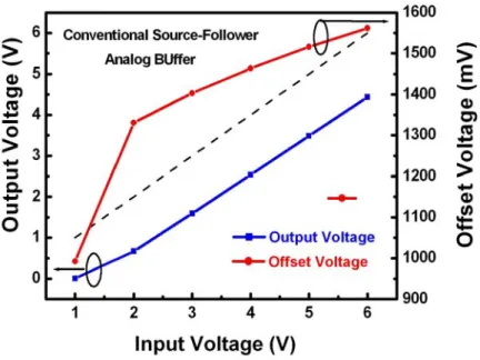
Figure 2.14 Conventional source-follower type analog buffer.
Figure 2.15 Simulation result of the output voltage and output offset voltage versus input voltage of conventional source-follower type analog buffer.
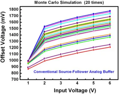
Figure 2.16 Monte Carlo simulation result of the output offset voltage of conventional source-follower type analog buffer.
Figure 2.17 Circuit configuration and timing diagrams of Chung’s push-pull analog buffer.
Figure 2.18 Simulation result of the output voltage and output offset voltage versus input voltage of Chung’s push-pull analog buffer.
Figure 2.19 Monte Carlo simulation result of the output offset voltage of Chung’s push-pull analog buffer.
Figure 2.20 Circuit configuration and timing diagrams of Sony’s double-offset-canceling analog buffer.
Figure 2.21 Simulation result of the output voltage and output offset voltage versus input voltage of Sony’s double-offset-canceling analog buffer.
Figure 2.22 Monte Carlo simulation result of the output offset voltage of Sony’s double-offset-canceling analog buffer.
Figure 2.23 Circuit configuration and timing diagrams of Jung’s analog buffer.
Figure 2.24 Simulation result of the output voltage and output offset voltage versus input voltage of Jung’s analog buffer
Figure 2.25 Monte Carlo simulation result of the output offset voltage of Jung’s analog buffer.
Figure 2.26 Structure of source follower with compensating capacitance.
Figure 2.27 Circuit configuration and timing diagrams of Yoo’s inverter type analog buffer.
buffer.
Figure 2.29 Simulation result of the output voltage and output offset voltage versus input voltage of Jung’s analog buffer.
Figure 2.30 Monte Carlo simulation result of the output offset voltage of Jung’s analog buffer.
Chapter 3
Figure 3.1 Layout image of conventional single channel TFTs and TFTs with multi-channel structure.
Figure 3.2 The process procedure of fabricating ELC LTPS TFTs.
Figure 3.3 Transfer characteristics of thirty LTPS TFTs at Vds = 0.1 V of (a) single channel devices, (b) multi-channel device with stripe number =5, and (c) multi-channel device with stripe number =10.Simple pixel circuit for AMOLED.
Figure 3.4 Output characteristics of thirty LTPS TFTs at Vg=10V of (a) single channel devices. (b) multi-channel device with stripe number =5, and (c) multi-channel device with stripe number =10.
Figure 3.5 Cumulative distributions of (a) threshold voltage, (b) substhreshold swing, and (c) transconductace the device parameters from 25 n-channel LTPS TFTS (W/L=10μm/5μm) of single channel structure and multi-channel structure.
Figure 3.6 Cumulative distributions of (a) threshold voltage, (b) substhreshold swing, and (c) transconductace the device parameters from 25 n-channel LTPS TFTS (W/L=200μm/5μm) of single channel structure and multi-channel structure.
Figure 3.7 Probable distributions of the relative location between grain structures and the devices. (a) single channel devices, and (b) multi-channel devices. Figure 3.8 SEM image of poly-Si thin films crystallized by ELA.
Figure 3.9 Conventional source follower and conventional source follower with multi-channel structure in the driving TFT.
Figure 3.10 Measured results of the output offset voltage variations in ten sets of conventional source follower buffer circuits.
Figure 3.11 Measured results of the output offset voltage variations in ten sets of conventional source follower buffers with multi-channel structure of the driving TFTs.
Figure 3.12 Comparison of the measured output offset voltage variations between the conventional source follower and conventional source follower with multi-channel structure.
Chapter 4
Figure 4.1 Conventional source-follower type analog buffer.
Figure 4.2 Simulating output waveform of conventional source-follower type analog buffer.
Figure 4.3 Schematic of conventional source follower with an active load and its output waveform simulating results.
Figure 4.4 Offset voltage comparison of conventional source follower and source follower with an active load in various charging time.
Figure 4.5 Cumulative distributions of the device parameters from 30 n-channel LTPS TFTS fabricated on the same glass substrate.
Figure 4.7 Twenty times of Monte Carlo simulation results of the conventional source follower with an active load when input voltage 2V to 4V.
Figure 4.8 Schematic and the timing diagram of the proposed source-follower-type analog buffer.
Figure 4.9 Monte Carlo Simulation output waveform of the proposed analog buffer when input voltage is 2V, 3V, 4V.
Figure 4.10 Optical micrograph of the proposed analog buffer circuit. Figure 4.11 Measurement system for the testing buffer circuits.
Figure 4.12 Measurement result of the offset voltage compared between the proposed analog buffer and the conventional analog buffer.
Figure 4.13 Offset voltage variation of 8 set of the analog buffer circuits are compared between the proposed analog buffer and the conventional analog buffer. Figure 4.14 Simulation result of the output offset voltage and the power dissipation for
the proposed analog buffer with different bias voltage.
Figure 4.15 Output offset voltage versus bias voltage of the measurement result in comparison with the simulation result at input voltage Vin=3V.
Figure 4.16 Output offset voltage versus bias voltage of the measurement result in comparison with the simulation result at input voltage Vin=2V.
Chapter 1
Introduction
---
1.1 Overview of the Applications of Thin Film Transistors
(TFTs)
Thin-film transistors (TFTs) have been widely used in the electronic system applications in the past ten years. Depending on the different materials of active layer, thin-film transistors (TFTs) can be mainly categorized to three types: amorphous silicon thin film transistors (a-Si:H TFTs), polycrystalline silicon thin film transistors (poly-Si TFTs), and organic thin film transistors (OTFTs). Amorphous silicon thin film transistors (a-Si:H TFTs) were introduced in the 1970’s, which have been used in many applications such as solar cells [1.1], image sensors, printing heads, electronic copiers [1.2]-[1.4], especially in the applications of active matrix liquid crystal displays (AMLCDs) [1.5]-[1.7] and newly developed active matrix organic light emitting displays (AMOLEDs) [1.8]-[1.10]. In the AMLCDs, a-Si:H TFTs is used as the pixel switch placed at each pixel for addressing. While in the AMOLEDs applications, a-Si TFTs is used as the active device to provide driving current for illumination. Although a-Si TFTs has the advantage of low processing temperature (<350oC) to allow the use of cheap, mass-produced glass substrate. However, the low carrier mobility of a-Si TFTs which is generally below 1cm2/V-s makes the
difficulty in realizing high resolution definition displays.
On the other hand, polycrystalline silicon (poly-Si) was used to be the active material of TFT for achieving higher performance in the 1980s. Poly-Si TFTs can be divided into two types according to the process temperature, which are high-temperature polycrystalline silicon TFT (HTPS TFT) and low-temperature polycrystalline silicon TFT (LTPS TFT). High- temperature poly-Si TFTs is fabricated by chemical vapor deposition (CVD) with processing temperature above 650oC. This approach requires an endured high-temperature substrate such as quartz, and this demand restricts to the small panel display such as projection display system which is inexpensive. Therefore, a low temperature process was investigated and progressed rapidly to be compatible with glass substrates for increasing economic benefits. Poly-Si TFTs fabricated with a maximum temperature below 600oC is so called low-temperature polycrystalline silicon thin film transistors (LTPS TFTs). In the fabrication of LTPS TFTs, the crystallization of a-Si thin film is considered to be the most important process. Among various low temperature crystallization methods, the excimer laser crystallization (ELC) is considered to be the most promising approach to get high performance of the transistors compared with solid phase crystallization (SPC), metal induced crystallization (MIC) [1.11]-[1.12]. Low temperature poly-Si TFTs can be applied to image sensors [1.13], solar cells [1.14], 3-dimension ICs’ [1.15], and the most conspicuous application is the pixel element [1.16]-[1.17] and integrated peripheral circuits of active matrix liquid displays (AMLCDs) [1.18]-[1.20]and active matrix organic light emitting displays (AMOLEDs) [1.21]-[1.22]. Because of the higher carrier mobility and better reliability, LTPS TFTs offer the possibility for integrating the peripheral circuits with the pixel array on a single glass substrate to realize the final target of system-on-panel (SOP) which integrating the driver circuits, controller circuits, memory, central process unit (CPU), etc., and achieve the compact, highly reliable, and low cost display system.
due to the advantages of very low process temperature (<200oC) and easily fabricated, therefore OTFTs can be fabricated on the flexible plastic substrate for low cost electronics applications. OTFTs can be applied to the switching devices for active matrix flat panel displays (AMFPDs) based on liquid crystal pixels(AMLCDs), organic light emitting diodes(AMOLEDs), or “electronic paper” displays [1.23]-[1.24], additionally, sensors [1.25], low-end smart cards, and radio-frequency identification tags (RFIDs) consisting of organic integrated circuits. Although OTFT can be applied to large area, low-temperature processing, structural flexible, and low cost applications, this technology is not mature yet [1.26]. Many issues limit the applications of OTFT such as device stability and lifetime, and the most critical issue of OTFTs is the extremely low field effect mobility (typically <<1cm2V-1s-1) compared to the a-Si TFTs and LTPS TFTs.
1.2 Comparison between Amorphous Silicon Thin Film
Transistors (A-Si TFTs) and Low-Temperature
Polycrystalline Silicon Thin Film Transistors (LTPS
TFTs)
In this section, we will compare the difference between the a-Si TFT and LTPS TFT from two aspects. First is the manufacturing aspect in terms of process steps, commercial cost, and yield and second is the electrical performance including the driving capability and stability.
z
Manufacturing aspect
z Process Steps and Commercial Cost
Less process steps, usually four to five mask processes are necessary for the fabrication of a-Si TFT which is usually employed by bottom gate structure. These mask processes include gate electrode, a-Si active layer, source/drain electrode, passivation layer, and ITO. Compared to a-Si TFT, top gate structure is usually adopted for LTPS TFTs, and more process steps, nine to ten mask process are needed. They are poly-Si active layer, channel and source/drain implant (N+, N-, P+), gate electrode, inter layer dielectric, source/drain electrode, passivation layer, and ITO.
In addition to more process steps, extra equipment is required to fabricate the LTPS TFTs. These include excimer laser annealing for poly-Si film crystallization, ion implanter or ion shower for implantation to form the source/drain, rapid thermal annealing or excimer laser annealing for doping activation. Consequently, higher equipment cost than a-Si TFT is required to fabricate LTPS TFT. More process steps and higher equipment investment make LTPS TFT more costly than a-Si TFT [1.28]
z Electrical Performance
z Driving Capability
Due to the smaller grain sizes and higher gate/source and gate/drain overlap capacitances of hydrogenated amorphous silicon TFT, the mobility of a-Si TFTs is generally below 1.0 cm2/V-s, and such low carrier mobility limits the driving capability of a-Si TFT. In order to meet sufficient driving capability, large W/L ratio must be designed in the a-Si TFT based circuits which limit the resolution of display. Besides, with the intrinsic properties of a-Si, only n-type TFT is available when a-Si is employed which greatly
reduces the flexibility of TFT applications and causes some difficulties in designing. On the other hand, the carrier mobility of LTPS TFT is one or two orders higher than that of a-Si TFT. The higher driving ability makes it a good candidate for high resolution displays, even provides the possibility of integrating driver circuits for AMLCDs and AMOLEDs to realize completely system on panel (SOP). Besides, both n-type and p-type LTPS are available, therefore CMOS drivers can be integrated on the substrate.
z Stability
A-Si TFT suffers from large threshold voltage shift and conductance current lowering after long term operation. These device performance degradations are commonly explained by two mechanisms which include the dangling-bond states creation in the amorphous silicon layer and charge trapping in the gate insulator [1.29]-[1.30]. On the other hand, LTPS TFT is quite stable relatively after a prolonged period of biasing time.
Although low temperature polycrystalline silicon thin-film transistors (LTPS TFTs) require higher manufacturing cost than that of a-Si TFT, the higher driving capability and better long term reliability of the LTPS TFT are more suitable for the flat panel display applications. At present, LTPS TFT has attract much attention for integrating driver circuits of active matrix liquid crystal displays (AMLCDs) and active matrix organic light emitting diodes (AMOLEDs) [1.31]-[1.32]. However, there are still some issues of LTPS TFTs for system-on-panel (SOP) application. The more detailed concepts and issues of system-on-panel (SOP) are discussed in the next section.
1.3 The Concepts and Issues of System-On-Panel (SOP)
At present, application of thin film transistors (TFTs) for active matrix display is mainly in the pixel element, the driving circuits and other controlling circuits of active matrix display are employed with single crystalline VLS IC design on printed circuit board (PCB). It requires large numbers of interconnections between the panel and the peripheral circuits. Since off-panel connections have considered to be the most frequent cause of LCD failure, the system-on-panel (SOP) technology which omitting the usage of ICs and interconnections promise the LTPS-based products to be more reliable. Moreover, reducing the number of external components and the connections to display enable to lower the cost of panel and a compact, light weight system can be achieved for better economic benefits. Thus, several researches have been proceeded to integrate the analogue and digital display driver circuits , controller circuits, random access memory (RAM), and more complicated part such as central processing unit (CPU) or digital signal processing (DSP) on the active matrix substrate [1.33]-[1.34]. In 2004, the first full-functional system panel was proposed by Sharp Corporation and Semiconductor Energy Laboratory Co., where a CPU, a graphic controller, an audio circuit, a program ROM, an audio ROM, various types of RAMs, a voltage generator, a clock generator, and the large-scale logic circuits comprising approximately 120,000 TFTs are monolithically formed on a glass substrate forming an LCD by using CG-Silicon technology [1.35].
Although the system display has been successfully demonstrated, the technology is not matured for mass production. In additional, the advantages of lower system cost and lower power consumption are not apparent nowadays. The properties of poly-Si TFTs are considered to be the key factors for the goal of system-on-panel, thus the disadvantages of electrical properties and the fabrication techniques of poly-Si TFTs must be improved to
satisfy the requests for system on panel. Here, several critical issues and the research opportunities for developing system on panel are discussed in the following sections.
z
Issues of System-On-Panel
z Electrical Properties
At present, the performance of poly-Si TFTs is still much poor in comparison with conventional single-crystal MOSFETs such as lower carrier mobility, higher threshold voltage, larger subthreshold current and larger leakage current, etc. In order to achieve high speed and high driving capability of poly-Si TFTs, significant advances in carrier mobility are needed. As the carrier mobility is improved, the scale of the transistors can be reduced without sacrificing the driving current, thus high integrated density of transistors can be obtained for high resolution and more functions integrated display system. For the demand of low power consumption, low and centered (between n-tpe TFT and p-type TFT) threshold voltage of poly-Si TFTs is needed. The high threshold voltage will result in relatively high voltage supply required to drive the circuits and dissipate high power.
The kink effect and hot carrier effect of poly-Si TFTs are also the critical problems in system display progressing. Kink effect of poly-Si TFTs causes the high value of output conductance and a strong dependence on bias condition [1.36] that will raise the difficulty in circuit design. For example, in analogue applications that will lead to a considerable reduction of the maximum attainable gain and reduces the common mode rejection ratio (CMRR), and result in increasing of power dissipation and slightly degrades the switching characteristics in digital circuits. Besides, the unsaturated I-V curve causes the problem in saturation voltage defined. The standard definition of saturation voltage is not applicable because a well-defined saturation does not exist. Hot carrier effect will cause the shift of
threshold voltage, subthreshold swing, and mobility of poly-Si TFTs due to the carrier trapped in the Si/SiO2 interface or carrier injection to the gate oxide. This will degrade the reliability of poly-Si TFTs. Moreover, in order to reduce the kink effect and hot carrier effect, device with drain-engineering architecture or some circuit configurations (e.g. cascode, normally used to reduce the consequences of the kink on circuits) must be introduced. Thus the added steps of device process and excessive number of stacked devices are required which result in an increase in fabricated cost and power dissipation.
The device electrical properties play a key role in the performance of display, therefore, electrical characteristics of poly-Si TFTs must be further improved for meet the requirements of next system-on-panel (SOP) generation.
z Uniformity
Over the past ten years, laser-based crystallization has been intensely studied and developed for poly-Si TFTs [1.37]-[1.40], and have been verified to be the excellent technology with the ability to produce high quality poly-Si films [1.41]. Excimer laser crystallization (ELC) is the most commonly used method for mass production of LTPS TFTs. However, the narrow process window of laser energy density for producing poly-Si thin film is a critical issue for ELC LTPS TFTs. In order to crystallize large-grain poly-Si, the laser energy density must be controlled in the super lateral growth (SLG) region. Nevertheless, the pulse-to-pulse variation of excimer laser energy density and non-uniform laser beam profile cause the laser energy density not to be uniformly controlled in the SLG region across the large area. That result in random grain boundaries distributed in the channel region of LTPS TFTs between devices. As the channel dimensions continue to shrink, the uniformity behavior becomes more severe. The larger device-to-device variation will lead to many problems in real product applications.
z Design Rule Consideration
The performance of poly-Si TFTs is inferior to that of conventional single crystallization Si MOSFETs at present. In order to keep compatible with large-area processing, relatively coarse design rules must been used in designing the poly-Si TFTs based circuits [1.41]. There are three reasons for this phenomenon. First of all, the restriction of photolithographic and processing for fabricating TFTs on the large-area substrate is severe. It is more challenging to scale down the device into the submicron dimension because of limitations in the resolution of lithography equipment. Second, the short-channel effects are relatively severe in poly-Si TFTs. As the dimension scaled down, the short-channel effects will intensely affect the device performance and make more difficulty in designing. Third, an AMLCD pixel typically requires a total voltage swing of about 10 V to encompass both the positive and negative driving polarities, and about 15 V supply voltage is needed by using poly-Si TFTs drivers. Therefore, the broader line width is required.
In order to enhance the device performance, the dimension of poly-Si TFTs must be scaled down. For the development of more advanced panels systems, the dimension of channel must be shrunk to submicron dimension (<0.8um) to achieve high performance TFTs [1.42]. However, there are many challenges to scale down the device into the submicron dimension domain by current mass production technologies. Thus it requires the development and introduction of new technologies of process and device.
z Power Consumption
poly-Si TFTs compared to single crystal Si MOSEFTs. It require higher supply voltage for sufficient driving capability of poly-Si TFTs, thus the power consumption of integrated driver circuits tends to be higher than that of single crystal silicon ICs. This tendency will increase as circuit-integration progresses. For example, in the case of QVGA (Quarter Video Graphics Array) LCDs, the power consumption of conventional TFT-LCD with external driver ICs ranges from 10 to 13 mW, while that of typical SOP-LCDs with integrated driver circuits ranges from 20 mW upwards, which is more than twice of the power consumption of conventional TFT-LCDs [1.43].
Therefore, power reduction is one of the major challenges in further advanced SOP-LCDs application. From the viewpoint of device electrical characteristics, low and centered (between nMOS and pMOS device types) threshold voltage with extremely small distribution is needed for meeting the requirement of low power consumption. Designing the driver circuits with simple configuration and less control signals is also a solution from the designing aspect. Furthermore, modified driver architecture and lowered the line resistance and parasitic capacitance are also the efficient methods to reduce the power consumption.
z Yield
At present, the fabrication cost of low-temperature poly-Si TFTs is higher than that of amorphous silicon TFTs because of more process steps and more expensive equipments. The reduction of external component cost has been offset by the higher fabrication cost in many commercial applications, resulting in higher display prices. Besides, the narrow process window of laser crystallization technology, and additional steps or more complex texture employed to achieve high performance poly-Si TFTs (ex. drain engineering for reducing the kink effect and hot carrier effect, additional steps or equipments for
crystallization to get high carrier mobility) will also reduce the production yield rate. Therefore, how to get high manufacturing yield is really important for real production applications.
z
Research Opportunities for Realizing System-On-Panel
To achieve the goal of system-on-panel, the improvements at various levels are required to solve several issues as discussed above. This can be achieved from three aspects: materials and process technology, device structure, and circuit design.
z Materials and Process Technology
New elemental process technology is needed for the formation of high quality critical
layers, such as the active and the gate-insulator layers of poly-Si TFTs. In the area of active layer, high quality poly-Si microstructure is needed to increase device
performance. The crystallization process is a very critical step of the fabrication process for TFTs, because it needs to satisfy the requirements on trade-off considerations including material quality, fabrication cost and thermal-budget constraints imposed by the display substrate. The key points for further improved poly-Si crystallization technology are high electrical performance and good uniformity which can be achieved through enlarging grain size, reducing the defect densities, getting good grain orientation and location control. Several advanced crystallization technology has been proposed to achieve large grain size or location controlled poy-Si film such as the “Continuous Grain Silicon (CG Silicon)” technology by Shrap Corporation [1.44]-[1.45], “Selectively enlarging laser crystallization (SELAX)” technology by Hitachi, Ltd. [1.46]-[1.47], or “comb-shaped excimer laser annealing” technology by NEC Corporation [1.48]-[1.50].
In terms of gate insulator layer, there are requirements in thickness and film quality - i.e. fixed and interface trap density, reliability against electrical stress. GI thickness reduction is necessary to get a TFT gate length in the submicron range. As GI thickness decreases, issues of step coverage become increasingly more severe. Current gate insulator technology is based on PECVD TEOS-SiO2, but this technology seems incapable of overcoming the challenge with the gate insulator thickness gradually decreasing to 50 nm and beyond. In order to maintain high quality for increasingly thinner gate insulator layer, new technology must be introduced.
z Device Architecture
Modified device architectures must complement and customize device performance according to required function. Improvements in the device architecture are vital in two aspects: (1) enable the fabrication of submicron channel dimensions with technology compatible with LCD manufacturing and (2) provide an additional way to complement material quality and compensate the variation of material properties in the critical layer for supplying additional controls for system optimization. But it must conform to the requirement of low cost, thus without extra process step (ex. additional steps for drain engineering or integration of low-voltage and high-voltage TFTs) is also taken into consideration.
z Circuit Design
In additional to improved process technology and device structure, improvements from the circuits design concept offer another solution to realize the goal of system-on-panel. For example, analog buffer which is indispensable to driving large load capacitance of the panel
will suffer from large offset voltage and huge output variation due to the high threshold voltage and large device-to-device variation of poly-Si TFTs. Precise circuit design is employed to deal with the output offset voltage and eliminate the output variation of the buffer circuits through the appropriate circuit architecture and driving scheme. To ensure designing accurately of circuits, suitable device model and exact device parameters are required. It is important to develop accurate models of poly-Si TFTs for circuit simulation and design.
1.4 Motivation
The “system-on-panel (SOP)” technology by low-temperature poly-Si thin-film transistors (LTPS TFTs) is considered to be the most promising solution for realizing the compact, highly reliable, fully functionally, and low system cost display because of the higher carrier mobility of LTPS TFTs which allow the integration of the driver circuit with pixel circuits on a single glass substrate. However, the severe device-to-device variation of LTPS TFTs due to the inevitable process such as pulse-to-pulse variation of laser energy density and random distribution of grain boundaries greatly restrict the progress of system-on-panel (SOP) technology. Thus, in this thesis, the electrical non-uniformity of LTPS TFTs is studied from two viewpoints: device structure and circuit design.
z The Effect of Multi-channel Structure on the Uniformity of LTPS TFTs
In this part, we purpose to improve the device non-uniformity of LTPS-TFTs from the aspect of device architecture by means of simply modifying the device architecture while without the use of additional masks and no need to modify the normal process of TFT
fabricating. The multi-channel structure with slicing layout method is used in this work. The electrical characteristics and uniformity of multi-channel devices are studied and compared to conventional single-channel devices. The mechanisms of improving uniformity by the multi-channel structure are found out according to the experimental results.
z Electrical Uniformity Compensation by Circuit Design
For the development of integrated data driver employing LTPS TFTs, output buffers are indispensable to drive the large load capacitance of data lines. However, the LTPS TFTs suffer from huge device-to-device variations that cause the bad uniformity of output voltage of analog buffers across the panel. Therefore, many researches on LTPS TFTs analog buffer have been tried to realize a buffer with high immunity to the device variations, and source-follower type analog buffer shows the superiority among these efforts. In additional to the large variations of electrical properties, LTPS TFTs have much larger subthreshold current compared with single crystal Si transistors, and this poor electrical characteristic will results to large output offset and cause the output voltage not to be constant with time. Thus in this thesis, we intend to design a new source-follower type analog buffer which can not only eliminate the output variations but suppress the output unsaturated phenomenon of conventional source-follower type analog buffer. The proposed analog buffer is composed of two n-type thin film transistors, one storage capacitor and four switches. The output voltage variation decreases greatly by the storage capacitor and compensated operation of the proposed buffer. Furthermore, the unsaturated phenomenon of output voltage arisen from the significant subthreshold current of driving TFTs is also eliminated by adding an active load. According to the simulated and measured results, it is obvious that the output voltage is very closely to the real input voltage and the output variations are successfully compensated in the proposed analog buffer.
1.5 Thesis Organization
In chapter two, two types of analog buffers employing low-temperature polycrystalline silicon thin film transistors are introduced and compared. These are operational amplifier type and source-follower type analog buffers. First, the circuit configuration and operation principle of both the simple structure op-amp buffers and modified op-amp circuits with compensated configuration are described. Next, the conventional source-follower type analog buffer and various compensated source follower circuits are introduced. The advantages and disadvantages of op-amp type and source-follower type analog buffers are compared in the end of this chapter.
In chapter three, the effects of the multi-channel structure on the device uniformity of LTPS TFTs are investigated and discussed. The possible mechanisms of improving uniformity of multi-channel structure are proposed and analyzed according to the experimental results. At last, the multi-channel structure is also introduced to the driving TFT of conventional source-follower type analog buffer to study its influence on circuit performance.
In chapter four, a novel source-follower type analog buffer composed of two n-type thin film transistors, a storage capacitor and four switches is proposed for improving the image quality of displays. An active load is employed to the buffer circuit to suppress the unsaturated phenomenon of output voltage arisen from the significant subthreshold current of driving TFTs. The threshold voltage compensation capability and the elimination of unsaturated output voltage phenomenon of the proposed analog buffer are verified by both the SPICE simulation results and experimental results. The measurement results of offset voltage and output variation of proposed analog buffer are also compared to the
conventional analog buffer circuits. Besides, the effect of bias voltage of active load on the performance of proposed buffer circuits is also discussed in this chapter.
Chapter 2
Overview of the Analog Buffer Circuits
Using Low-Temperature Polycrystalline
Thin Film Transistors
---
2.1 Introduction
Researches on “system-on-panel” technology have been attracted much attention at present because it provides a chance to realize a compact, light weight, high reliability, and low cost display system [2.1]-[2.3]. Low-temperature polycrystalline silicon thin film transistor is considered to be the best candidate for carrying out system display due to the low temperature process, high carrier mobility and the compatibility to CMOS technology, which allow the integration of the driver circuit and even more complicated parts such as controller circuits, random access memory (RAM), and central processing unit (CPU) with pixel circuits on a single glass substrate. However, LTPS TFTs suffer from huge device-to-device variation due to the pulse-to-pulse variation of laser energy density and random distribution of grain boundaries, such poor uniformity makes the difficulty to fully integrate driving circuit using LTPS TFTs.
To realize integrating driving circuits using LTPS TFTs, output buffers are indispensable for the data driver to drive the large load capacitance of data lines. However, the poor uniformity of LTPS TFTs leads to the non-uniformity of buffer output voltage
across the panel which results in the wrong image displaying. Therefore, many researches employing LTPS TFTs have been tried to carry out analog buffers with high immunity of the device variations [2.4]-[2.17].
Analog buffer circuits using LTPS TFTs are classified into operational amplifier type (op-amp type) analog buffer and source-follower-type analog buffers according to their circuit architecture. Operational amplifier is most commonly used as the output buffer in single crystal silicon integrated circuits. However, the complicated circuit configuration and the huge output voltage variation of op-amp-type analog buffer using LTPS TFT make it not suitable for system-on-panel application. Source-follower-type analog buffer is considered a better candidate because of its simplicity and higher immunity to the device variations of LTPS TFT.
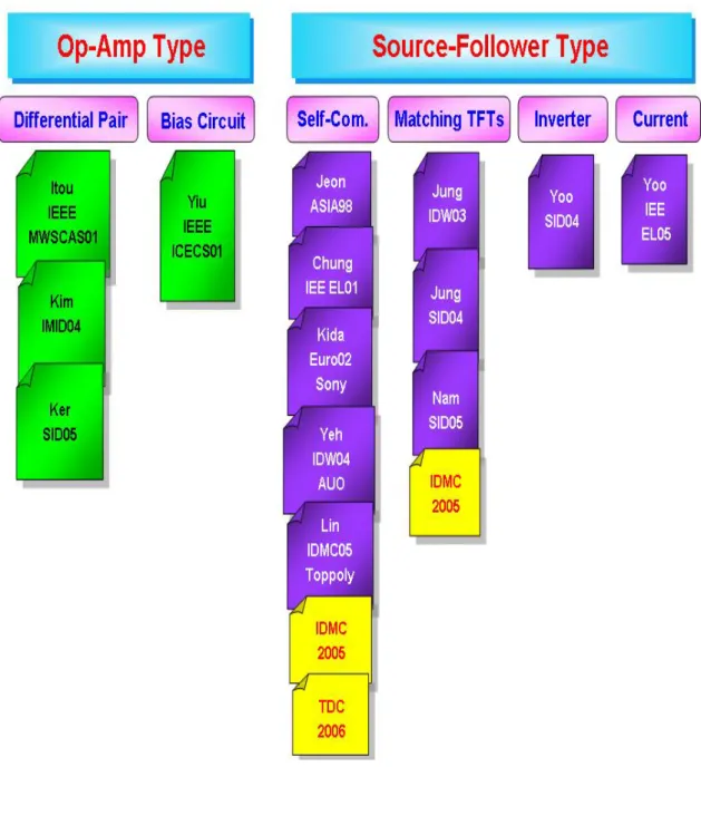
In this chapter, the circuit configuration, operating sequence, advantages and disadvantages of these two types of LTPS TFT analog buffers circuits are introduced. Those analog buffer circuits are simply classified into various types as shown in Fig. 2.1 based on the compensated methods [2.4]-[2.19]. The compensation principles of different types with configuration will be described in detail in this chapter. Furthermore, the output characteristics of the op-amp type analog buffer circuits and source-follower type analog buffer circuits are also discussed in this chapter.
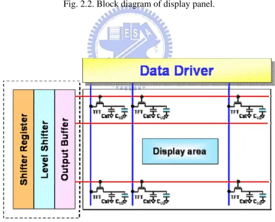
2.1.1 Architecture of AMLCD Driver
The block diagram of AMLCD display panel is shown in Fig. 2.2. The periphery circuits blocks of LCD panel are composed of scan driver, data driver, timing controller, DC/DC converter, gamma reference voltage driver, common voltage driver (Vcom driver). The timing controller decodes the output waveform to generate control signals at corresponding time, which is responsible for controlling the behavior of scan driver and transmitting the RGB (red, green, and blue) signals to the data driver. A DC-DC converter steps up a single externally supplied voltage to various higher level voltages (ex. VDD to 2VDD, 3VDD positive output voltage, and -2VDD, -3VDD negative output voltage) which provide the power supply voltage to the timing controller, interface circuit, source driver, gate driver, reference voltage driver and common voltage driver [2.20]-[2.21]. The gamma reference voltage driver is used to provide the various gamma reference voltages to the digital-to-analog converter (DAC) circuits. The common voltage driver is used to provide the common electrode voltage for the panel. Besides, the scan driver and data driver will be further discussed in the following.
z Scan Driver
The scan drivers generate the scan pattern and turn on each scan line sequentially. The architecture of source driver is shown in Fig. 2.3. It consists of shifter register, level shifter, and output buffer. The shift register is used to store digital input signal and transit them to the next stage, which generates sequential scan pulse for scan line according to the timing clock. The function of the level shifter is to translate the digital signal to a higher level voltage because the higher voltage is needed to turn on the switch element of the active pixel. Since the scan lines can be modeled as RC (resister and capacitor) ladder, the output
buffer is indispensable to drive the RC loading.
z Data driver
Fig. 2.4 shows the architecture of data driver which mainly contains shifter register, data register, level shifter, digital to analog converter (DAC) and output buffer. The first three stages are categorized as digital part, and the other two stages are belonged to analog part. The shift register generates pulse signal for video signal sampling according to the clock signal and transmit the pulse digital RBG signals to the next stage [2.22]. The data register receives the serial data signal and transmits them in parallel. The function of the level shifter is the same as the one used in the scan driver. It is applied to converter the digital RGB signal to a higher level voltage for data driver [2.23]. Because the data signal is transmitted in the digital interface, the digital to analog converter (DAC) is needed to convert the digital RGB video data into analog data signal for displaying the gray level [2.24]-[2.25]. Finally, the selected video data is transmitted to the data line after changing impedance in the output buffer. The purpose of output buffer is to assure the active pixels can be driven into a desired gray level. When the digital to analog converter is insufficient for driving the large loading of data line, the output buffer is used to enhance its driving capability. As the output buffer is applied, the DAC will charge a smaller loading of output buffer instead of a larger loading of data line. Thus, the desired data signal can be transmitted to the active area accurately. Because the LCD panel usually has large loading, especially in larger panel or higher resolution display, the analog buffer is indispensable to drive the large loading of the data lines.
Fig. 2.2. Block diagram of display panel.
Scan Driver
TFT Cst CLC TFT Cst CLC TFT Cst CLC TFT Cst CLC Display area Display area TFT Cst CLC TFT Cst CLCActive Matrix Panel
Bi-directional Shift Register Data Register
Analog Buffer
Digital to Analog Converter Level Shift
Analog Part Digital Part
Scan DriverScan Driver
TFT Cst CLC TFT Cst CLC TFT Cst CLC TFT Cst CLC TFT Cst CLC TFT Cst CLC TFT Cst CLC TFT Cst CLC TFT Cst CLC TFT Cst CLC TFT Cst CLC TFT Cst CLC Display areaDisplay areaDisplay area
Display area TFT Cst CLC TFT Cst CLC TFT Cst CLC TFT Cst CLC TFT Cst CLC TFT Cst CLC
Active Matrix Panel
Bi-directional Shift Register Bi-directional Shift Register
Data Register Data Register
Analog Buffer Analog Buffer
Digital to Analog Converter Digital to Analog Converter
Level Shift Level Shift
Analog Part Digital Part
Fig. 2.4. Architecture of the data driver.
2.1.2 Design Considerations for LTPS-TFTs Analog Buffer
To design the output buffer for the data driver of flat pane display, there are several critical issues to be considered. These include output voltage accuracy, driving capability, layout area, and power consumption.
(1)
Output voltage accuracy
: Analog buffer is applied to the data driver for ensuringthat the data signal outputted from DAC can be transmitted exactly to the active pixel. Thus, the high output voltage accuracy of analog buffer circuits is required to display the desired gray level correctly.
(2)
Driving capability:
The output settling time for the data drivers must be fast enough to quickly transfer the data signals into the pixels within a line time. Therefore, the analog buffers in the end of data driver must quickly charge or discharge the load capacitance of data bus. Especially in the larger panel area and higher resolution display, the line time becomes shorter while the loading of data line is large. High driving capability of the output buffer is needed to achieve fast transition time and to get sufficient capability for driving large loading of data lines.(3)
Layout area:
For the LAAT (line at a time) driving architecture, one analog buffer is needed for each column line. Thus, several hundreds of analog buffers are needed in active matrix display. As the resolution is higher and higher in the future, the amount of analog buffers is increasing and larger area will be occupied. Moreover, a data driver should fit in one pixel pitch, and circuit layout area is limited. Therefore, the simple configuration and less transistors are pursued for high-resolution display.(4)
Power consumption:
The power consumption of poly-Si TFT integrated circuitstends to be higher than that of single-crystalline silicon ICs because of inferior electrical characteristics of poly-Si TFT such as higher threshold voltage, lower carrier mobility. For the expanding market of mobile and portable production, the demand of power dissipation is increasing. Since several hundreds of analog buffers are needed in the LAAT (line at a time) driving architecture, large static power is dissipated of analog buffers. Therefore, it needs to design an analog buffer with low power consumption.
2.2 Op-amp-type Analog Buffer
2.2.1 Typical Op-amp-type Analog Buffer
Operational amplifier (op-amp) is generally connected as an unit-gain buffer to act as the output buffer in the single crystal silicon LSIs. A typical two-stage operational amplifier (op-amp) is composed of a differential amplifier and an output stage as shown in Fig. 2.5.
Fig. 2.5. Simple two-stage op-amp unit gain buffer.
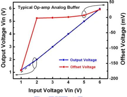
The output voltage versus input voltage characteristic and output offset voltage of a typical two-stage op-amp unit-gain buffer employing LTPS TFTs are shown in Fig. 2.6, where the offset voltage is defined as the difference between the input voltage and output
voltage, (i.e. Voffset=Vinput -Voutput ). The simulation result shows the good linearity of the op-amp unit-gain buffer. The output offset voltage is average under 30 mV expect when the input voltage is in low level where the offset voltage may exceed 150mV.
Fig. 2.6. Simulation result of the offset and output voltage versus input data voltage for typical two-stage op-amp type analog buffer circuit.
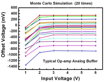
Although the output error of the typical op-amp type analog buffer is small, huge output voltage variation may exist in this circuit because of the inevitable non-uniformity of the poly-Si TFTs electrical characteristics, such as threshold voltage and mobility variations. In order to study the effect of device non-uniformity on the circuit performance, Monte Carlo simulation with an assumption of normal distribution is introduced where the mean value and deviation of the threshold voltage and the mobility are 1.45V, 0.5V and 65.69 cm2/V-sec, 15 cm2/V-sec, respectively. Each poly-Si TFTs are assumed to vary independently when the Monte Carlo simulation is executed. Fig. 2.7 shows the Monte Carlo simulation results of the two-stage op-amp unit gain buffer. It is obvious that the
output voltage has huge variations, where the variation of output offset voltage may get up to 1450mV. This serious output variation makes it difficult to design a high performance output buffer with the typical op-amp-type analog buffer. Therefore, some compensating methods have been proposed to solve this problem. These compensating methods for op-amp type analog buffer will be discussed in the next section.
Fig. 2.7. Monte Carlo Simulation result of the typical op-amp-type analog buffer with input voltage varying from 1V to 6V.
2.2.2 Op-amp-type Analog Buffer with Compensated
Architecture
The compensating methods for device-to-device variation of LTPS-TFTS op-amp-type analog buffer can be mainly classified into two kinds including differential pair compensated method and bias circuit compensated method. The concepts and operating method of these two kinds of compensating circuits will be discussed in detail.
2.2.2.1 Differential Pair Compensated Method
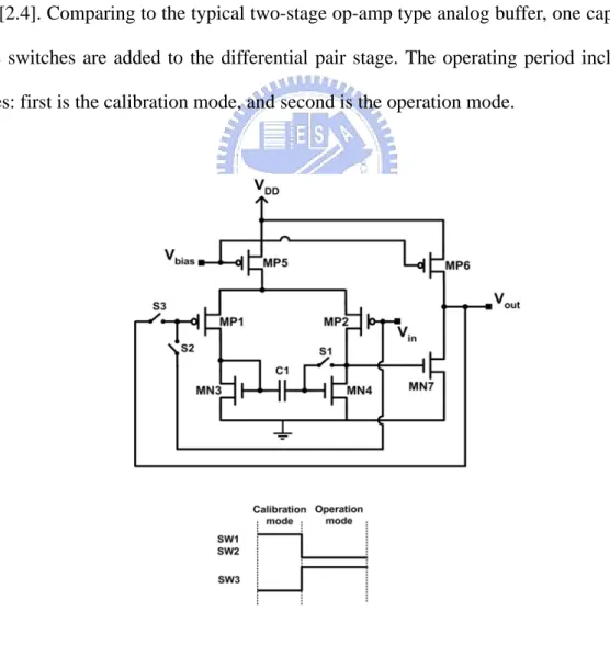
For the differential pair compensated method, an additional capacitor is used to compensate the device mismatch of the differential pair stage. The operating period usually includes two stages. First is the period to calibrate the electrical properties mismatch of the differential pair and the second stage is the signal data voltage programming period. Fig. 2.8 shows an example of this type of compensating method. The op-amp-type unit gain buffer with threshold voltage and mobility deviation-free differential amplifier was reported by Itou [2.4]. Comparing to the typical two-stage op-amp type analog buffer, one capacitor and three switches are added to the differential pair stage. The operating period including two stages: first is the calibration mode, and second is the operation mode.
Fig. 2.8. Circuit configuration and timing diagram of Itou’s differential amplifier compensated op-amp-type unit gain buffer.
In the calibration mode, switches S1 and S2 are on, and S3 is off. At this time, the two input voltages of the differential pair (MP1, MP2) are the same, and the difference of gate to source voltages between the active load pair (MN3, MN4) is stored in the capacitance C1. The gate voltage of the active load is corresponding with the threshold voltage of the differential pair and the active load. Therefore, the differential pair mismatch and the load pair mismatch are stored in the capacitance C1. When the switches S1 and S2 are off, and S3 is on, the circuit is in the operation mode. In this mode, the input data is transmitted to the output stage. Since the differential pair mismatch and the load pair mismatch have been recorded in the first stage, the input offset resulting from device mismatches can be fully canceled in the operation mode. Thus, the final output voltage will be close to the input data signal in this buffer circuits.
Fig. 2.9. Simulation result of the offset and output voltage versus input data voltage for Itou’s differential pair compensated op-amp-type analog buffer circuit.
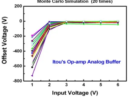
The output performance of Itou’s op-amp analog buffer has been studied by simulation results. Fig. 2.9 shows the output voltage-input voltage characteristic and the output offset of the buffer. The output deviation is small except in low input data signal. The Monte Carlo
simulation result is also shown in Fig. 2.10. It is obvious that the output offset variation of this buffer circuits is much smaller than that of the typical two-stage op-amp-type analog buffer. However, the output variation still remains large (~550mV) in low input data level. It is because that when the input data is in low level, the two transistors of the differential pair (MP1, MP2) operate in the linear region. Thus, the transconductance (gm) of two transistors of the differential pair are not kept in constant which result to the differential pair mismatch and the load pair mismatch cannot be recorded accurately in the capacitance C1 and result in the output performance sensitive to the device variation. Besides, the mismatch of the output stage of the analog buffer also contributes to the output variation of the Itou’s op-amp-type analog buffer.
Fig. 2.10. Monte Carlo Simulation result of the Itou’s op-amp-type analog buffer with input voltage varying from1V to 6V.
2.2.2.2 Bias Circuit Compensated Method
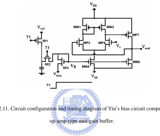
voltage generating circuit is applied to eliminate the influence of threshold voltage variation on the bias current. Fig. 2.11 shows an example of op-amp-type analog buffer using this compensating method [2.7]. This buffer circuit is composed of a typical two-stage op-amp unit gain buffer and the threshold voltage insensitive gate bias generating voltage.
Vg
Fig. 2.11. Circuit configuration and timing diagram of Yiu’s bias circuit compensated op-amp-type unit gain buffer.
The bias current of this op-amp can be expressed as :
2 d o x 5 _ 5 _ 1 I C ( ) ( 2 M N g s M N t h M N W V V 5) L μ = − (2.1)
When there is large variation in threshold voltage that will causes bias current variation, thus the variation of gm (transconductance). This in turn causes the non-uniformity of the buffer circuit characteristics across the panel. Therefore, eliminating the effect of threshold voltage variation on bias current may maintain the output characteristics of the op-amp unit-gain buffer. Thus, Yiu propose a gate voltage biasing circuit to provide an insensitive bias gate voltage Vg, (refer to Figure. 2.10) for biasing the transistors. The operation of this
compensating circuit is described in the following. In the first stage, the transistor M1 turns on, and the capacitor will be charged up to Vref. Then transistor M1 turns off and transistor M2 turns on to connect the capacitor to transistor M3. Since transistor M3 is connected like a diode, it will discharge the capacitor until the gate voltage of the transistor M3 is equal to Vbias + Vth. Then this voltage is applied to the gate of MN5, MN6 to provide the bias current: 2 d o x 5 _ 3 _ 5 1 I C ( ) ( 2 M N b i a s ) W V Vt h M N Vt h M N L μ = + − (2.2) and 2 d o x 6 _ 3 _ 6 1 I C ( ) ( ) 2 M N b i a s t h M N W V t h M N V V L μ = + − (2.3)
The bias current will be independent of the threshold voltage of the transistor if the transistor MN3, MN5 and MN6 are matched. Therefore, the output non-uniformity of the op-amp type analog buffer resulting from the bias current fluctuation can be eliminated in this compensating circuit architecture.
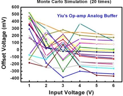
Fig. 2.12 and Fig. 2.13 show the simulation results of the output offset voltage and the output variation versus input data voltage, respectively. It is clear that large output variation still remains in this compensating circuit. It means that the electrical performance variations can not be calibrated out in this compensating architecture. It is because that the compensating method is performed in the bias circuits but not the differential pair. Even if the bias current mismatch has been compensated, the device mismatch of the differential pair and the active load pair which are the mainly causes of output variation for op-amp-type unit gain buffer still remain. Besides, the compensating configuration will
work effectively only when the electrical characteristic MN3, MN5 and MN6 are matched, but it is very difficult to achieve completely device matched between transistors. In addition to large output variation, extra setup time is also required for the application of this buffer circuit to generate the threshold voltage insensitive bias voltage. Furthermore, op-amp-type analog buffer needs many transistors which not only occupy large area but cause high power dissipation. Therefore, the op-amp-type analog buffer is not suitable for the driver integration applications.
Fig. 2.12. Simulation result of the offset and output voltage versus input data voltage for Yiu’s bias circuit compensated op-amp-type analog buffer circuit.
Fig. 2.13. Monte Carlo simulation result of theYiu’s op-amp-type analog buffer with input voltage varying from1V to 6V.