國 立 交 通 大 學
電子工程學系 電子研究所碩士班
碩 士 論 文
具有四相位電壓控制震盪器用在超寬頻帶
頻率合成器的互補式金氧半導體鎖相迴路
CMOS Phase Lock Loop with Quadrature
Voltage-Controlled Oscillator for Ultra
Wide Band (UWB) Frequency Synthesizer
研 究 生:許晏維
指導教授: 吳重雨 博士
具有四相位電壓控制震盪器用在超寬頻帶頻率合成器的
互補式金氧半導體鎖相迴路
CMOS Phase Lock Loop with Quadrature
Voltage-Controlled Oscillator for Ultra Wide Band (UWB)
Frequency Synthesizer
研究生: 許晏維
Student: Yen-Wei Hsu
指導教授: 吳重雨 博士
Advisor: Dr. Chung-Yu Wu
國 立 交 通 大 學
電 子 工 程 學 系
碩 士 論 文
A Thesis
Submitted to Department of Electronics Engineering & Institute of Electronics College of Electrical and Computer Engineering
National Chiao Tung University in partial Fulfillment of the Requirements
For the Degree of Master In
Electronics Engineering October 2008
HsinChu, Taiwan, Republic of China 中華民國九十七年十月
具有四相位電壓控制震盪器用在超寬頻帶
頻率合成器的互補式金氧半導體鎖相迴路
研究生: 許晏維
指導教授: 吳重雨 博士
國立交通大學
電子工程學系 電子研究所碩士班
摘要
具有超寬操作頻率高傳輸速率由 IEEE 802.15 TG3a 制定的超寬頻通訊系統已被 視為次世代通訊系統的主軸。在最近幾年,7128-MHz 附近的頻帶中,已有 7.5-GHz 的 頻寬由美國國家通訊委員會(FCC)釋出作為高速短距離通訊系統使用。此頻帶具有可 應用在高達數百-百萬位元等級的高傳輸速率無線個人網路(WPAN)以及點對點傳輸的 潛力. 此論文中介紹了一個應用在超寬頻帶的全頻帶頻率產生的系統結構和其中的一 個有兩級環式震盪器的鎖相迴路電路實現。此全頻帶頻率產生的系統中包含了使用最 少數目的 SSB 混波器、統一的輸出級以及兩個固定除數的鎖相迴路等電路並且使用了 0.13-um CMOS 技術來設計。藉由使用兩級的環式震盪器,所需要的操作頻率不需要額 外的電路而可以容易的達到,且環式震盪器具有高度的整合性。進一步來說,在 IC 中它可以節省更多的功率消耗和晶片面積。本電路的輸出相位雜訊在 1 MHz 偏差下是 -117.6 dBc/Hz 而功率頻譜是-0.313 dBm。在 1.2-V 的電源下,當震盪器輸出在所需 的頻率 7128 MHz 時,其直流的功率消耗是 12.42 mW。而頻率可以調整的範圍在控制電壓 1.1 V~0.1 V 時,是 5.8 GHz~8.8 GHz。
除了震盪器電路,除頻器電路是在不同的操作頻率下選擇不同的的電路架構以節 省功率的消耗。而相位頻率偵測器是使用一般的結構並且在操作頻率 500 MHz 以下都 可以正確的工作。而充電幫浦的充放電流不匹配比率在控制電壓 1.1 V~0.1 V 時,都 在 4 %以下。最後的迴路濾波器是由國家半導體提供的程式來設計的二階濾波器,並 由 Matlab 寫的程式來做二次驗證已求其相位極限(phase margin)大於 60 度。在預估 輸出負載在 100 fF 下,整個鎖相迴路所消耗的功率大約是在 29 mW,頻道內的突波抵 抗程度是-53dBc。
CMOS Phase Lock Loop with
Quadrature Voltage-Controlled Oscillator
for Ultra Wide Band (UWB) Frequency
Synthesizer
Student: Yen-Wei Hsu
Advisor: Dr. Chung-Yu Wu
Department of Electronic Engineering &
Institute of Electronics
National Chiao Tung University
Abstract
In the next-generation wireless communication as UWB applications, high data rate transmission with a wide operating frequency spectrum is expected to be realized by 802.15.3a Task Group specification. Over the past few years, the 7.5-GHz frequency spectrum divided into 14 bands around 7128 MHz has been released by FCC for unlicensed use in high-speed and short-range communication systems. It has great potential in application of high data-rate wireless personal–area network (WPAN), high speed WLAN and point-to-point link, with possible data rate of hundreds of megabits per second.
In this thesis, a full-band frequency spectrum generation scheme for UWB applications and a phase lock loop with two-stage ring oscillator are presented. The proposed full-band
frequency spectrum generation scheme which consists of the least single-side-band mixers, a unified output port, and two division-number fixed PLL. The higher output frequency PLL is designed by using 0.13-um CMOS technology. Utilizing a two-stage ring oscillator, the operating frequency of the PLL can be achieved effortlessly without other circuit component. It also has high integration for ICs. Furthermore, it saves more power consumption and chip area in integrated circuits. The output phase noise of the oscillator is -117.6 dBc/Hz at 1 MHz offset and the power spectrum is -0.313 dBm. The power consumption of the two-stage ring oscillator is 12.42 mW from 1.2-V power supply at the required output frequency 7128 MHz. The tuning range of the oscillator is 5.8 ~8.8 GHz under 1.1~0.1 control voltage.
Besides oscillator, the divides are chosen different architectures for different operation frequencies to economize on power consumption. Phase and frequency detector is using the conventional structure that cost small power consumption and could function correctly under operation frequency 500 MHz. The mismatching ratio of the proposed current-match charge pump is 4 % under the control voltage 0.1V~1.1V. Finally, the loop filter is designed by the loop filter design software from National Semiconductor as second order structure and double check with Matlab code to let the phase margin higher than 60 degrees. The overall power consumption of the proposed PLL is around 29 mW at estimation output loading 100 fF. The in band spur rejection is -53 dBc.
ACKNOWLEDGEMENTS
首先,感謝我指導教授,吳重雨老師,一直以來對我的耐心指導與諄諄教誨,讓 我能夠順利完成碩士學業。猶記得剛進電子研究所時,對於類比電路相關研究的陌生 與無力感,深怕自己無法勝任繁複的電路研究,過程中遇到種種挫折與失敗,多虧老 師的鼓勵與教誨,透過與老師的討論與指導,可以循序漸進,完成此論文。還有師母 曾昭玲女士,能夠給予我精神上的鼓勵與支持,讓我能在挫折中再重新向前努力。在 積體電路設計上,再次感謝我的老師吳重雨博士以他淵博的專業知識,給予我信心與 毅力,在遇到瓶頸的時候,適時的予我幫助與啟發,並透過由老師建立起的 307 實驗 室,充足的設備且環境的薰陶,還有學長姊的專業,讓我充分學習到分析電路的技巧 。其次要感謝論文口試的評審委員,郭建男教授、高宏鑫博士與周忠昀博士對我的論 文提出了許多寶貴的建議,使這篇論文的內容更加完整。還有實驗室的其他老師,許 炳堅榮譽教授,吳介琮教授、柯明道教授與陳巍仁教授,您們所建立起在電子領域中 的成就,可供我們做為永遠的模範。僅在此表達對您們最崇高與深切的謝意。 接下來要感謝實驗室的眾多學長姐們,不論是在生活上或是研究的課題,你們總 是給予我不求回報的幫助!僅此感謝 307 實驗室的學長姊,首先是博士班部份的:林 俐如學姊、王文傑學長、虞繼堯學長、蘇烜毅學長、陳旻珓學長、黃祖德學長、陳勝 豪學長、蔡夙勇學長、黃鈞正學長、王仲益學長、曾偉信學長、吳書豪學長、張智閩 學長、盧台祐學長、陳建文學長、張瑋仁學長、顏承正學長、蕭淵文學長、王暢資學 長、賴泰翔學長與王資閩學長等學長們給予我的指教幫忙和研究上的經驗傳承。還有 碩士班學長姊:李宗霖學長、未曾謀面的張家華學長、EMMY 學長、歐欣華學長、楊宗 熙學長、夏志朋學長、黃傑忠學長、吳建樺學長、吳諭學長、鄭鍵樺學長、POLO 學長 、余岱原學長、小幾丸學長、紅毛學長、粘家熒學長、石弼嘉學長、羅怡凱學長、詹 豪傑學長、孫汝玉學姊、張志遠學長、李允斌學長、謝仲朋學長、黃必超學長、郭豐 偉學長、廖昌平學長、高立龍學長、徐國慶學長、王志賢學長、胡芳綾學姊、陳佳惠 學姊、沈宛儀學姊等學長姊們,受到你們的幫助太多,可以回饋的卻太少,僅在此再 次獻上我最誠摯的感謝。尤其是王文傑學長、虞繼堯學長、蘇烜毅學長、陳旻珓學長 、黃祖德學長、羅怡凱學長、郭豐偉學長和余岱原學長對我的碩士論文題目的指導,沒有你們就沒有我的論文。 同時也要感謝我的好同學們維德、國忠、順維、柏宏、廷偉、松諭、巧伶、宗裕 、世豪、鯉魚、小王,做我低潮時的避風港,陪伴我度過這段溫馨的研究生活,增添 了許多歡笑與回憶;還有幫忙我許多的學弟妹們:萬諶、國權、鎮邦、威宇、建銘、 筱妊、威文、有儀、宗恩、昕華、國維、晟佑、國軒、介堯、柏硯、世範、惠雯、謝 謝你們,也祝福你們能在電子的領域中發光、發熱。還要謝謝我在研究所生涯所結識 的好朋友們:諭哥、怡凱、汝玉、小王、鯉魚(和女朋友)、國忠、順哥、維德、神童 、Hakko、豪哥(小的那個)、萬諶、松諭、巧玲、宗裕、岱原、TAKA、188、ddlink、 志朋(和女朋友)、傑忠(和女朋友)、朱哥等。和你們一起度過的這幾年,是我人生中 永難忘記的歲月。 最後也要感謝我的父母親,感謝你們一直體諒我的任性,並給予我莫大的鼓勵, 讓我可以在沒有壓力的環境下,選擇自己所走的路,完成碩士的學業。還要感謝我所 有親戚、好友們,你們的支持是我一路走來最堅定的力量。需要感謝的人太多,也希 望自己所得到的恩惠能夠有可以回報的一天。最後祝福大家身體健康,平安如意。 許晏維 誌於 風城交大 2008 秋
Contents
ABSTRACT (Chinese)……….………...…....iii
ABSTRACT (English)………...v
ACKNOWLEDGEMENTS...vii
CONTENTS…….…..……….………..……...ix
FIGURE CAPTIONS……….………...………....xi
TABLE CAPTIONS……….………...…….….xiv
Chapter 1 Introduction……….1 1.1 Background………11.2 Reviews of MB-OFDM UWB Synthesizer………...……3
1.2.1 UWB Synthesizers………...6
1.3 Motivation………....14
1.4 Thesis Organization……….15
Chapter 2 A 3.1~10.6 GHz CMOS Frequency Synthesizer………...…16
2.1 Multi-Band OFDM Physical Layer Proposal for IEEE 802.15 Task Group 3a...…16
2.2 Frequency Planning……….19
2.2.1 Frequency Planning Architecture………..20
2.3 System Design Consideration………..………22
2.4 UWB Frequency Synthesizer Architecture and Operational Principle………27
2.5 Discussion and Comparison……….29
Chapter 3 Phase Lock Loop Theory and System Simulation………....31
3.1 Basic Considerations………31
3.2 Phase-Lock-Loop Architecture………...….36
3.2.1 Integer-N Architecture………37
3.2.2 System Specifications………...…...38
3.2.3 Phase Noise Analysis………...……40
3.3.1 Design Consideration……….……….43
3.3.2 System Simulation……….………..45
3.3.3 Settling Time and Reliability of PLL………56
Chapter 4 Quadrature Oscillator Based PLL…...………....60
4.1 Quadrature voltage-controlled Oscillator…………...………...61
4.1.1 Operational Principle………...………..62
4.1.2 Design Consideration………..67
4.1.3 Circuit Realization………..74
4.2 Prescaler and Dividers………...81
4.2.1 Operational Principle………...…..81
4.2.2 Design Consideration………..83
4.2.3 Circuit Realization………...85
4.3 Phase and Frequency Detector……….89
4.3.1 Operational Principle……….90 4.3.2 Design Consideration………..92 4.3.3 Circuit Realization………..93 4.4 Charge Pump………95 4.4.1 Operational Principle……….95 4.4.2 Design Consideration………..97 4.4.3 Circuit Realization………100 4.5 Loop Filter……….105 4.5.1 Design Consideration………105 4.6 Summary of the 7128-MHz PLL ……….……….110 4.7 Summary of the 3168-MHz PLL ………...……….113
Chapter 5 Conclusion and Future Work………...116
5.1 Conclusions………116
5.2 Future Work………117
Figure Captions
Figure 1.1 The architecture of the phase lock loop...4
Figure 1.2 The architecture of the many PLLs as each band’s synthesizer...5
Figure 1.3 The block diagram of the [4]’s full-band frequency planning...6
Figure 1.4 The circuit block diagram of [4]...7
Figure 1.5 The block diagram of the [5]’s full-band frequency planning...8
Figure 1.6 The circuit block diagram of [5]...9
Figure 1.7(a) The circuit block diagram of [6]...10
Figure 1.7(b) The diagram of the [6]’s full-band frequency planning...11
Figure 1.8 The block diagram of the [7]’s full-band frequency planning...12
Figure 1.9 The circuit block diagram of [7]...13
Figure 2.1 Frequency planning of MB-OFDM UWB systems...16
Figure 2.2 Frequency switching for each symbol of a MB-OFDM UWB burst...18
Figure 2.3 Third-order spurious tones are out of 7.5 GHz spectrum for UWB application...19
Figure 2.4 The block diagram of proposed frequency planning architecture for UWB applications...21
Figure 2.5 The block diagram of the example frequency algorithm...21
Figure 2.6 Frequency synthesizer in a MB-OFDM UWB transceiver...22
Figure 2.7 Effect of unwanted frequency translation of interferers...26
Figure 2.8 The proposed 3.1~10.6 GHz frequency synthesizer for MB-OFDM UWB application...27
Figure 2.9 The block diagram of the frequency spectrum generation scheme...28
Figure 3.1 The (a) ideal, (b) actual output spectrum of an oscillator...32
Figure 3.2 The effect of phase noise in (a) the receive path, (b) the transmit path...33
Figure 3.3 The (a) spurs, (b) effect of spurs in receive path...35
Figure 3.4 The feed-through of the reference frequency...36
Figure 3.5 A simple charge pump PLL as frequency synthesizer...37
Figure 3.6 The proposed PLL architecture...39
Figure 3.7 Noise sources of type II 3rd PLL linear model...40
Figure 3.8 System considerations for each block of PLL...44
Figure 3.9 Phase noise performance of roughly simulated VCO...46
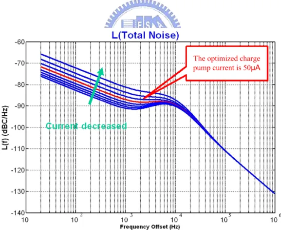
Figure 3.11 The variation of output phase noise with different charge pump current...49
Figure 3.12 The circuit architecture of loop filter...51
Figure 3.13 The open loop Bode plot of PLL...52
Figure 3.14 PLL loop filter design by the software...54
Figure 3.15 The Bode plot of the PLL designed by the software...55
Figure 3.16 The PLL behavior model by Simulink...56
Figure 3.17 The locking time of the PLL from initial state to the output wanted frequency...57
Figure 3.18 The Bode Plot of the open loop transfer function...58
Figure 3.19 The Bode Plot of the open loop transfer function with (a) +30% (b) -30% variations...59
Figure 4.1 The architecture of the integer-N PLL in this work...61
Figure 4.2 The architecture of the (a) single ended (b) differential output ring oscillators...63
Figure 4.3 The architecture of the even number stages ring oscillator with RC equivalent delay...64
Figure 4.4 The conceptual block diagram of the proposed two-stage ring oscillator...65
Figure 4.5 The differential delay cell: (a) circuit diagram, (b) frequency response...68
Figure 4.6 The differential delay cell with partial positive feedback: (a) circuit diagram, (b) frequency response...69
Figure 4.7 The first version of the designed differential delay cell...70
Figure 4.8 The half circuit of the designed differential delay cell...71
Figure 4.9 The small signal equivalent model of (a) the half circuit (b) with rearrangement...72
Figure 4.10 The circuit diagram of the proposed two-stage ring oscillator and the oscillator buffers...74
Figure 4.11 The frequency response of the proposed differential delay cell...75
Figure 4.12 The input and output signals in differential delay cell with only one input signal...76
Figure 4.13 The transient results of the ring oscillator at 7128 MHz...77
Figure 4.14 The phase noise of the two-stage ring oscillator...78
Figure 4.15 The tuning range of the two-stage ring oscillator...78
Figure 4.16 The output spectrum of the two-stage ring oscillator...79
Figure 4.17 The tunung range of the two-stage ring oscillator at 7128 MHz under TT, FF and SS corner...80
Figure 4.18 The architecture of the D flip-flop based divide_by_2 frequency divider...82
Figure 4.19 The architecture of the D flip-flop based divide_by_3 frequency divider...82
Figure 4.20 The circuit diagram of the D flip-flop for the divide_by_2 frequency dividers...84
Figure 4.22 The simulated waveforms of (a) prescaler, and (b) divide_by_2 frequency divider...86
Figure 4.23 The simulated waveforms of (a) the first, (b) the second, and (c) the last divide_by_3 frequency dividers...88
Figure 4.24 The simulated waveforms of the ring oscillator and the divide_by_108...89
Figure 4.25 The characteristic of the phase and frequency detector...90
Figure 4.26 The conceptual operation of phase and frequency detector...91
Figure 4.27 The state diagram of the tri-state phase and frequency detector...91
Figure 4.28 The structure of the tri-state phase and frequency detector...92
Figure 4.29 The structure of the TSPC D-type flip-flop in phase and frequency detector...93
Figure 4.30 The simulated waveform of phase and frequency detector at (a) divided frequency leading to reference frequency, and (b) divided frequency lagging reference frequency...94
Figure 4.31 The block diagram of the PFD and charge pump with the timing diagrams...96
Figure 4.32 The current-match charge pump architecture used in this work...97
Figure 4.33 (a) The feedback loop of the charge pump, and (b) the equivalent circuit of the loop...98
Figure 4.34 The proposed current-match charge pump with solved start-up problem...101
Figure 4.35 (a) The simulation results of the proposed PFD and charge pump, and (b) the control line of the oscillator in charging case...102
Figure 4.36 (a) The simulation results of the proposed PFD and charge pump, and (b) the control line of the oscillator in discharging case...103
Figure 4.37 The mismatching ratio of the charge pump between charging and discharging currents...104
Figure 4.38 The (a) loop filter design, and (b) Bode plot of the proposed PLL by the software...107
Figure 43.9 The Bode Plot of the open loop transfer function simulated by Matlab...108
Figure 4.40 The Bode Plot of the open loop transfer function with (a) +30% (b) -30% variations simulated by Matlab...109
Figure 4.41 The phase relation between quadrature phase of oscillator...110
Table Captions
Table 1.1 The summary and comparison of the UWB application and other communication standards...3
Table 2.1 The summary of the UWB frequency synthesizer specifications...26
Table 2.2 The summary and comparison of the UWB frequency synthesizer characteristics...29
Table 3.1 The expected specification for proposed PLL...39
Table 3.2 The parameters for analyzing the loop filter...54
Table 3.3 The final parameters of the PLL in this work...55
Table 4.1 The summary and comparison of the proposed oscillator...80
Table 4.2 The summary and comparison of the PFD for the important characteristics...94
Table 4.3 The summary and comparison of the CP for the important characteristics...104
Table 4.4 The parameters for the loop filter...106
Table 4.5 The summary of the 7128-MHz PLL...112
Table 4.6 The summary of the 3168-MHz PLL...114
Chapter 1
Introduction
1.1 Background
Over the past few decades, wireless communication systems have been under significant development and are more closely related to our daily life than ever before. In the digital home of the not-too-distant future, people will be sharing photos, music, video, data and voice among networked consumer electronics, PCs and mobile devices throughout the home and even remotely. Users will be able to stream video content from a PC or consumer electronics (CE) device -- such as a camcorder, DVD player or personal video recorder -- to a flat screen HDTV (high-definition television) display without the use of any wires.
A leading candidate for enabling this capability is ultra wideband (UWB), a wireless technology designed for high data-rate and low power consumption.
Traditional radio transmissions have a significant difference between UWB radio transmissions. It is that traditional systems transmit information by varying the power level, frequency, and/or phase of a sinusoidal wave. UWB transmissions transmit information by generating radio energy at specific time instants and occupying large bandwidth thus enabling a pulse-position or time-modulation. UWB pulses can be sent sporadically at relatively low pulse rates to support time/position modulation, but can also be sent at rates up to the inverse of the UWB pulse bandwidth. Pulse-UWB systems have been demonstrated at channel pulse rates in excess of 1.3 giga-pulses per second using a continuous stream of UWB pulses, supporting forward error correction encoded data rates in excess of 675 M bit/s.
One of the valuable aspects of UWB radio technology is the ability for a UWB radio system to determine "time of flight" of the direct path of the radio transmission between the transmitter and receiver at various frequencies. This helps to overcome multi path propagation, as at least some of the frequencies pass on radio line of sight. With a cooperative symmetric two-way metering technique distances can be measured to high resolution as well as to high accuracy by compensating for local clock drifts and stochastic inaccuracies.
Another valuable aspect of pulse-based UWB is that the pulses are very short in space (less than 60 cm for a 528 MHz wide pulse, less than 23 cm for a 1.3 GHz bandwidth pulse), so most signal reflections do not overlap the original pulse, and thus the traditional multipath fading of narrow band signals does not exist. However, there still is multipath propagation and inter-pulse interference for fast pulse systems which can be mitigated by coding techniques.
Ultra-Wideband (UWB) may be used to refer to any radio technology having bandwidth exceeding the lesser of 528 MHz or 20% of the arithmetic center frequency, according to Federal Communications Commission (FCC). A Report and Order by the FCC authorizes the unlicensed use of UWB in 3.1–10.6 GHz. The FCC power spectral density emission limit for UWB emitters operating in the UWB band is -41.3 dBm/MHz. This is the same limit that applies to unintentional emitters in the UWB band, the so called Part 15 limit [1].
Deliberations in the International Telecommunication Union Radiocommunication Sector (ITU-R) have resulted in a Report and Recommendation on UWB in November of 2005. National jurisdictions around the globe are expected to act on national regulations for UWB very soon. Other national regulatory bodies apparently are somewhat reluctant to allow common unlicensed use. More than four dozen devices have been certified under the FCC rules, the vast majority of which are radar, imaging or locating systems. UWB is making the transition from laboratories to standardization, a key step toward the development of
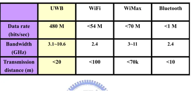
real-world products. The brief summary and comparisons of the UWB application and other communication standards are listed in the Table 1.1 below.
Table 1.1 The summary and comparison of the UWB application and other communication standards.
UWB WiFi WiMax Bluetooth
Data rate (bits/sec) 480 M <54 M <70 M <1 M Bandwidth (GHz) 3.1~10.6 2.4 3~11 2.4 Transmission distance (m) <20 <100 <70k <10
It is a tough task to grasp the analog and high frequency character in RF circuit design. Much more problems and issues we are facing than we expected. We all need to pay more efforts and time to get advancement. Through this way, we can make the world more convenient and comfortable as well as the motivation of our endeavors.
1.2 Reviews of MB-OFDM UWB Synthesizer
A frequency synthesizer is an electronic system for generating any of a range of
frequencies from a single fixed oscillator. They are found in many modern devices, including radio receivers, mobile telephones, radiotelephones, walkie-talkies, CB radios, satellite receivers, GPS systems, etc.
Frequency synthesizers used in commercial radio receivers are largely based on
phase-locked loops or PLLs. Many types of frequency synthesizer are available as integrated circuits, reducing cost and size. High end receivers and electronic test equipment use more sophisticated techniques, often in combination.
A phase locked loop does for frequency what the Automatic Gain Control does for voltage. It compares the frequencies of two signals and produces an error signal/frequency which is proportional to the difference between the feedback frequency and reference/input frequency. The error signal is used to drive a voltage-controlled oscillator (VCO) which creates an output frequency. The output frequency is fed through a frequency divider back to the input of the system, producing a negative feedback loop. If the output frequency drifts, the error signal will increase, driving the frequency in the opposite direction so as to reduce the error. Thus the output is locked to the frequency at the other input. This input is called the reference and is derived from a crystal oscillator, which is very stable in frequency. Fig 1.1 below shows the basic elements and arrangement of a PLL based frequency synthesizer.
Figure 1.1 The architecture of the phase lock loop
However, in MB-OFDM UWB system, it is somehow different from the above
GHz and fast switching time less than 9.47ns (that will be mentioned at chapter 2) cannot be attained by only one PLL. It is supposed to have a wideband character or multiple switched circuits used to work at various frequency bands, and more than one single carrier frequency is required in the receiver and transmitter. Besides, we cannot ignore the out-of-band
distortion that should be taken into consideration and analyzed.
By carefully investigating the UWB frequency synthesizer, the frequency switching time is the most difficult issue. How to let the frequency band change to the other frequency band cannot be solved only tuning the PLL’s output frequency. That is because the settling time of PLL is much more than 9.47ns. One of the solutions is to construct as many PLLs as the frequency bands you use [2], [3] as figure 1.2 circumscribed below. However, as the frequency bands extending and frequency planning groups growing, it is costly and
impractically in many applications. Some recently published works have been designed based on many frequency bands and less chip space. They will be discussed in subsequent sections.
1.2.1 UWB Synthesizers
As UWB synthesizer is evolving continuously, several main architectures have been generalized. These architectures are mainly toward full-band frequency synthesizer that may be extended to or already achieve the goal. Be sure that the complete frequency synthesizer of UWB system should be the quadrature phase output. The followings are representative reviews of the state-of-the-art UWB frequency synthesizers.
A 3-to-8-GHz Fast Hopping Frequency Synthesizer [4]
This paper has accomplished a 9-band (the whole bands is 14) frequency synthesizer, and it provide an architecture that can extend to achieve a full-band frequency synthesizer. The frequency planning rules will be clearly explained and analyzed in the chapter 2. Please allow me analyzing the paper’s frequency planning algorithm first. The following figure 1.3 is the architecture that how it achieve the full-band frequency planning.
Figure 1.3 The block diagram of the [4]’s full-band frequency planning
Its idea is to generate three basic bands by the first circle. Then generate the spacing frequency (528 MHz) and double spacing frequency (1056 MHz). From the basic frequency, it can extend to upper or lower frequency bands by adding or subtracting the one or double spacing frequency to cover the 14 bands. The realization of circuit block diagram is in the
following figure 1.4.
Figure 1.4 The circuit block diagram of [4]
As you see in figure 1.4, the first PLL’s output signals through the divide-by-2 or tri-mode divider generate the signal 12.5fB and the ±5fB ( fB is 528 MHz). Then the two signals through the single-side-band MixerA produce the three basic bands in the figure 1.3 (7.5fB=3960 MHz, 12.5fB=6600 MHz, 17.5fB=9240 MHz). The second PLL generates the two signals 4fB and 2FB. By frequency selector and tri-mode divider, the signals become the one, double or dc spacing frequencies (±2fB=± 1056 MHz, ± fB=± 528 MHz or dc=0 MHz) called extending frequency. Finally, through single-side-band MixerB, the basic bands and the extending frequency can cover the full-band of the UWB specifications.
The disadvantage of this architecture is the divide-by-2.5 in the first PLL hard to implement at first. Second, the single-side-band MixerB must operate over very wide frequency (from 3960 to 9240 MHz basically). It’s difficult to realize the circuit single-side-band MixerB by TSMC 0.18 μm processing technology. Because of that, this paper only implements only the two basic bands that cover 3 to 8 GHz.
A 14-band Frequency Synthesizer for MB-OFDM UWB Application [5]
This paper is the first implementation of the full-band frequency synthesizer by CMOS 0.18 μm process. We will first describe the frequency planning algorithm, and then analyze the block diagram of the circuit implementation. The following figure 1.5 is the architecture that how it achieve the full-band frequency planning.
Figure 1.5 The block diagram of the [5]’s full-band frequency planning
Its idea is to generate the fundamental band at 3960MHz of the 1st Group. Then we generate the extending frequencies 1584 MHz, 3168 MHz, 6336 MHz as extending frequency A, 528 MHz as extending frequency B, and extra 1584 MHz as extending frequency C. The fundamental band can extend to cover 1st Group by extending frequency B, or cover 2nd, 3rd or 5th Group by using extending frequency B first and then using extending frequency A. Finally, it can cover the 4th Group by using extending frequency B first, then using extending frequency A, and extending frequency C at last. For example, if you want to get the frequency band 8184 MHz, you should let the fundamental band subtract the extending frequency B (528 MHz) as band 3432 MHz first. Second, the band 3432 MHz adds the extending frequency A (6336 MHz) as 9768 MHz. Finally, the band 9768 MHz subtracts the extra extending frequency C (1584 MHz) to the band 8184 MHz we expect.
Figure 1.6 The circuit block diagram of [5]
The circuit block diagram realization is on the above figure 1.6. It generates the fundamental band (3960 MHz) by the first PLL and the other extending frequencies are generated by PLL2. By using the single-side-band (SSB) Mixer1, the 1st Group band frequencies would be achieved. The 2nd, 3rd, and 5th Group band frequencies would be produced through the SSB Mixer2 through the selection of the extending frequency chosen by the multiplexer. The last 4th Group band frequencies would be generated at the output of the last SSB Mixer3. That will cover the whole full-band frequency planning.
Although this paper’s algorithm of frequency planning avoids the mixers operating at wide frequency range, the extra mixer is used. It costs more passive component wasting chip area and power dissipation. Mixers also generate the spurs at the in-band/out-band that let the spur specification worse. Further more, it increases the complexity of the circuit that the integration of the system would be more difficult.
A 1.5V UWB Frequency Synthesizer Design [6]
This thesis is the first implementation of UWB frequency synthesizer in our research group ICS LAB. It let the old specification of the UWB frequency planning realized by TSMC CMOS 0.18μm process. Although the rules of UWB frequency planning are changed now, it still has the value of reference. There is the figure 1.7 of circuit block diagram below.
° 90 ° 0 ° 90 ° 0 ° 90 ° 0 ° 90 ° 0
Figure 1.7(a) The circuit block diagram of [6]
The frequency planning algorithm is that only one PLL generates the highest frequency band (10032 MHz). Then it divides the highest frequency to other extending frequencies (9504 MHz, 3168 MHz, 1056 MHz, and 528 MHz). Through the SSB Mixer1 and SSB Mixer2, the whole frequency bands would be produced to cover the full-band frequency planning. The frequency generation is signed on the figure1.8 below.
Figure 1.7(b) The diagram of the [6]’s full-band frequency planning
In order to cover the full-band planning, there is a mixer used in the PLL. It not only increases the risk of PLL’s locking problem, but also generates the spurs in output of PLL. It both increases the chip area and the power consumption, and the complexity become great issues. The PLL’s VCO is simple complementary LC tank structure that serves with only differential output signals not quadrature ones. It is forced to provide a poly phase filter to generate quadrature phase output. However, the poly phase filter is hard to design precisely that it cannot tolerate the frequency drifting from the VCO. The passive component of poly phase filter not only costs the area but also easily drifts in the chip process. There are three poly phase filter used in the architecture that may cause huge variations.
The architecture’s output is not integrated to one that cannot be integrated to receiver or transmitter. Different outputs also hard to measure the switching time of changing the
frequency bands. There is still one point it didn’t achieve that it is not a quadrature phase output. Transceiver is needed the quadrature phase output as LO signals. Although it is not perfect architecture, it only uses one PLL that saves a lot of chip area and power consumption.
A 3-to-10 GHz CMOS Frequency Synthesizer for MB-OFDM UWB system [7] This paper is the second implementation of UWB frequency synthesizer in our research group ICS LAB. It is realized by the TSMC CMOS 0.18μm process. It completely covers the UWB full-band frequency planning. The following figure 1.8 is the full-band frequency planning diagram of it.
Figure 1.8 The block diagram of the [7]’s full-band frequency planning
Its idea is to generate the fundamental frequencies (not the central frequency bands in UWB specification) at 8448 MHz, and 4224 MHz. Then it generates the extending frequencies 1848 MHz, 1320 MHz, 792 MHz, and 264 MHz as extending frequencies. The two fundamental frequencies can extend to cover the whole full-band frequency planning by adding or subtracting the extending frequencies. For example, if you want to get the frequency band 7128 MHz, you should let the fundamental frequency 8448 MHz subtract the extending frequency 1320 MHz to the band 7128 MHz we expect.
Figure 1.9 The circuit block diagram of [7]
The circuit block diagram realization is on the above figure 1.9. It generates the fundamental frequencies (8448 MHz, and 4224 MHz) by the output of PLL and the first divider-by-2 (Div1). Then the left dividers-by-2 (Div2~Div5) produce the other half frequencies each by each to get the signals 2112 MHz, 1056 MHz, 528 MHz, and 264 MHz. In order to produce the extending frequencies, we let the signals produced from dividers-by-2 circuits (Div2~Div5) add or subtract the reference frequency 264 MHz. We can get the extending frequencies 1848 MHz (2112 MHz-264 MHz), 1320 MHz (1056 MHz+264 MHz), 792 MHz (528 MHz+264 MHz), and the 264 MHz itself by using SSB Mixer1. The 1st Group and 2nd Group would be covered by the SSB Mixer2, and the 3rd Group, 4th Group, and 5th Group would be achieved by the SSB Mixer3. To get the quadrture phase output, the replica circuits (All the circuits besides PLL) should be constructed symmetrically as Q-path (Quadrature phase path) or I-path (In phase path).
The only disadvantage of this paper is the added mixer compared with other architecture. The affection it brought is as we mentioned in the second full-band architecture [5]. Although this, the paper still provides the best UWB full-band frequency synthesizer solution. No doubt the paper is chosen to publish in the IC’s highest sanctuary, International Solid-State Conference 2008.
Well, the CMOS frequency synthesizers covering as much UWB bands as fewer circuit components attract more and more attentions. It is placed huge emphasis on low-chip-area, lower-power, and higher-integration applications. The trend is ongoing all the time.
1.3 Motivation
As mentioned above, some published frequency synthesizers for UWB applications have been developed and surveyed. These frequency synthesizers require huge amount of chip area to satisfy the UWB specification. They not only use a lot of passive elements but also waste extra circuit components. Using a high efficiency frequency planning architecture would thoroughly solve these difficult positions. The architecture of the frequency synthesizer for UWB full-band applications would try to realize in TSMC 0.13μm process under 1.2-V supply voltage. The constructing circuit components would consist of the phase-lock-loop with a quadrature two-stage ring oscillator without inductors to save space. The system simulation and the design reliability of phase-lock-loop would be considered carefully.
The frequency synthesizer is fulfilled to IEEE 802.15 TG3a specification, which specifies a frequency switching time less than 9.47ns as fast hopping. It basically must cover the 14 bands from 3.1~10.6 GHz, and have quadrature phase outputs.
1.4 Thesis Organization
Chapter 2 describes the detailed specification of IEEE 802.15 Task Group 3a, design consideration of the UWB frequency synthesizer, and the proposed a 3.1~10.6 GHz UWB full-band frequency synthesizer is introduced. In Chapter 3, the circuit components of the phase-lock-loop are considered: phase and frequency detector, charge pump, and two-stage quadrature ring oscillator. The system simulation of a phase-lock-loop is also brought up. The chapter 4 shows the implementation of the circuits in phase-lock-loop. The design consideration of each component would be illustrated and theoretic analyzed. It would be made together with simulation results. Finally, the conclusion and future work are presented in chapter 5.
Chapter 2
A 3.1~10.6 GHz CMOS Frequency Synthesizer
To get a thorough understanding of the UWB system, the physical layer proposal for IEEE 802.25.3a is introduced and analyzed. The system design consideration, the theoretical analysis, as well as architecture of the proposed frequency synthesizer are discussed and presented in chapter 2.
2.1 Multi-Band OFDM Physical Layer Proposal for IEEE
802.15 Task Group 3a
The IEEE 802.15 TG3a [8] specifies the unlicensed 3.1~10.6 GHz UWB band for short-range and high data-rate communications. The specified frequency width 7.5 GHz spectrum is divided into 5 groups and 14 bands with spacing 528MHz as shown below in figure 2.1.
3432 3960 4488 5016 5544 6072 6600 7128 7656 8184 8712 9240 9768 10296
1st Group 2nd Group 3rd Group 4th Group 5th Group
MHz MHz MHz MHz MHz MHz MHz MHz MHz MHz MHz MHz MHz MHz #1 #2 #3 #4 #5 #6 #7 #8 #9 #10 #11 #12 #13 #14 7128 MHz 528MHz 4.125MHz #8
The band frequencies are given as follow: [9]
Band central frequency = 2904+528×Nb(MHz) Nb =1...14 (2-1) = 528×Nb'(MHz) Nb'=6.5...19.5
(2-2) where N represents band numbers, and b N represents the numbers of spacing frequency. b' Band #1~ Band #3 are used for Mode 1 application (mandatory mode), while Mode 1 and Band #6~ Band #9 are as Mode 2 application (optional mode). The remaining channels are reserved for future used. The UWB system provides a wireless PAN with data payload communication capabilities of 55, 80, 110, 160, 200, 320, and the fastest 480 Mb/s. It incorporates orthogonal frequency division multiplexing (OFDM) modulation using quadrature phase shift keying (QPSK), a technique that uses multiple carriers to mitigate the effect of multipath path fading. In order to satisfy the QPSK application, the signals in UWB system are different from conventional communication system. Quadrature phase signals must be applied in whole UWB system surely including frequency synthesizer.
The divided bands bandwidth is 528 MHz which is also divided into 128 sub-carriers resulting in a sub-carrier bandwidth is 4.125 MHz as shown in figure 2.1. Among the 128 sub-carriers, 100 tones carry payload data, 12 pilot tones facilitate coherent detection against frequency offset, 10 guard tones relax filter design and the other 6 null tones carry no
information at all.
The MB-OFDM system adopts a frequency-hopping scheme to provide frequency diversity and multiple accesses. The performance of such MB-OFDM UWB architecture in multipath is fundamentally limited by the energy capture ability because when the TX/RX switches to demodulating the subsequent sub-band [9], [10], [11], it loses any ability to
capture the multipath dispersed energy from the current sub-band. Thus, in order to improve the energy capture, pulsed multiband UWB systems need slower time-frequency hopping, i.e., longer contiguous symbol transmissions in each sub-band. This has naturally led to OFDM instead of pure pulse modulation in each sub-band due to the former’s inherent robustness to multipath.
Figure 2.2 Frequency switching for each symbol of a MB-OFDM UWB burst
Multiple piconet coexistence is enabled in multiband UWB systems by introducing channelization via use of suitably designed frequency-hopping sequences over the set of sub-bands as in fig. 2.2 above—in principle, depending on the channel environment and desired data rates, the hop rate can be slow (multiple symbols sent on one sub-band prior to band switching) or fast (only one symbol sent per sub-band). The frequency-hopping sequences are designed to minimize “collision” events when two users in different piconets simultaneously use the same sub-band—such cases lead to erasure of the transmitted symbols. Thus, the number of simultaneously operating piconets that can be supported by this approach depends on the availability of frequency-hopping sequences with one coincidence property. A guard interval of 9.47ns (5/528MHz) is given as TX/RX switching time, which essentially specifies the maximum frequency synthesizer settling time when hopping between
multi-bands.
Therefore, we know the two essential factors for UWB frequency synthesizer different from the conventional synthesizer. That is the fast hopping time for the TX/RX switching time, 9.47ns, and the quadrature phase output signals for QPSK application as TX/RX LO signals.
2.2 Frequency Planning
The architecture of the frequency planning for UWB systems application is quite important. Our frequency planning for MB-OFDM UWB application provides a great improvement of decreasing the chip area and spurious response. This frequency generation scheme makes the third-order unwanted sidebands caused by mixing fall outside the 7.5 GHz spectrum so that the lower spur level is achieved. The third-order frequencies of spurious tones are given as:
f1 = 3⋅fRF − fLO and f2 = 3⋅ fLO − fRF (2-3) where all the third-order spurious tones are out of the 7.5 GHz spectrum as fig 2.3 below.
As a result of this, the better frequency planning we used, the less circuit components and system disadvantages are revealed. As we mentioned in chapter 1 section 2, the reviews of the UWB frequency synthesizers, all the frequency planning architecture published have the goals to achieve themselves. Some of them want to subtract the number of the too many PLLs to decrease the chip area, some want to reduce the spurious response by subtracting the number of the SSB mixers, and so on ….. Every frequency planning algorithm for UWB frequency synthesizers earns its benefits for their goals, but it also brings the imperfection affecting the other property. Therefore, how to be universally satisfied is a huge challenge to get over. The followings are the frequency planning diagram of the UWB frequency synthesizer.
2.2.1 Frequency Planning Architecture
The frequency planning diagram is to generate the fundamental band at 7128MHz of the 3rd Group. Then we generates the extending frequencies 1584 MHz, 3168 MHz as extending frequency A, and 528 MHz as extending frequency B. The fundamental band can extend to cover 3rd Group by extending frequency B, or cover 1st, 2nd, or 5th Group by using extending frequency B first and then using extending frequency A. It is quite uncomplicated and directly perceived through the senses as shown in fig 2.4 below.
Figure 2.4 The block diagram of proposed frequency planning architecture for UWB applications
For example, if you want to get the frequency band 8184 MHz, you should let the fundamental band 7128MHz subtract the extending frequency B (528 MHz) as band 6600 MHz first. Second, the band 6600 MHz adds the extending frequency A (1584 MHz) to the band 8184 MHz we expected. All the frequency bands can be obtained by the two steps. This is much more simple and convenient to cover full-band spectrum than [5]. The block diagram of the above example frequency algorithm (fig 2.5) is as follow.
6600 7128 7656 8184 8712 9240 3rd Group 4th Group MHz MHz MHz MHz MHz MHz #7 #8 #9 #10 #11 #12 +1584MHz 6600 7128 7656 8184 8712 9240 3rd Group 4th Group MHz MHz MHz MHz MHz MHz #7 #8 #9 #10 #11 #12 PLL1 -528MHz goal
The advantage of this frequency generation scheme would be discussed and compared with other published architectures in the last session.
2.3 System Design Consideration
UWB frequency synthesizer is quite dissimilar to conventional narrow band ones in some aspect: I/Q output phase, data rate, operating bandwidth, co-existence with other standards… and so on. Therefore, the system design consideration should be modified to get the appropriate features of it. Preliminarily, single-ended circuits take the priority for its low power consumption and smaller chip area as compared to differential ones, though it is liable to suffer from higher noise and second-order distortion.
Fig. 2.6 above [12] illustrates the role of a UWB frequency synthesizer in an MB-OFDM direct conversion transceiver. As in other wireless systems, the frequency synthesizer has the crucial function of generating the local oscillator (LO) signal that drives the down-converter in the receiver path and the up-converter in the transmitter. There are at least two demanding requirements that make a frequency synthesizer for an MB-OFDM UWB radio significantly different from the widely explored synthesizers for narrow-band wireless systems, which are: 1) the range of frequencies to be generated spans several gigahertz and 2) the time to switch between different band frequencies within a band group should be less than 9.47 ns. This requirement prevents the use of a standard PLL-based synthesizer as a solution for this application.
In addition to the frequency switching speed, the synthesizer’s output LO signal must comply with other requirements to ensure proper operation of the MB-OFDM UWB radio. The specifications outlined here assume the OFDM parameters and bit error rate (BER) requirements described in [3] for a 480-Mb/s data transmission and an additive white Gaussian noise (AWGN) channel. A quadrature phase-shift keying (QPSK) constellation is considered for the individual sub-carriers. For a packet error rate of 8% with a 1024-byte packet, the target BER when using a coding rate
4 3 =
R is 10−5, which corresponds to an
un-coded BER of approximately 10−2. The complete characteristics over the entire frequency
bands and analysis are discussed below:
(1) Phase Noise
The phase noise from the LO in an OFDM receiver has two different effects on the received symbols. It introduces a phase rotation of the same magnitude in all of the sub-carriers and creates inter-carrier interference (ICI) [13]. The first undesired effect is eliminated by introducing pilot carriers with a known phase in addition to the
information carriers. On the other hand, phase noise produces ICI in a similar way as adjacent-channel interference in narrow-band systems. Assuming that the data symbols on the different sub-carriers are independent, the ICI may be treated as Gaussian noise. The power spectral density (PSD) of a locked PLL can be modeled by a Lorenzian spectrum described by [13]
( )
2 1 2 2 β β π ⋅ + = Φ f f (2-4)where β is the 3-dB bandwidth of the PSD, which has a normalized total power of 0 dB.
The degradation ( D in decibels) in the signal-to-noise ratio (SNR) of the received sub-carriers due to the phase noise of the LO in an OFDM system can be approximated as [14] O S N E T D ⋅ ⋅ ⋅ ⋅ ≅ 4π β 10 ln 6 11 (2-5)
where T is the OFDM symbol length in seconds (without the cyclic extension), β defines the Lorenzian spectrum described above, and
O S
N E
is the desired SNR for the received symbols (in a linear scale, not in decibels). For this system, 1 =4.125
T MHz and the O S N E
for the target coded BER of 10 is 5.89 (7.7 dB). For D=0.1dB and the mentioned parameters, β can be computed with (2-4) and is 7.7 kHz. The
corresponding Lorenzian spectrum has a power of -86.5 dBc/Hz @ 1 MHz.
(2) In Phase (I) and Quadrature Phase (Q) Matching
In an OFDM system, the amplitude and phase imbalance between the I and Q channels transform the received time-domain vector into a corrupted vector r , which
consists of a scaled version of the original vector r combined with a term proportional to its complex conjugate r . This transformation can be written as [15] ∗
riq =α⋅r+β⋅r∗ (2-6)
where αand β are complex constants, which depend on the amount of IQ imbalance. This alteration on the received symbols can have a significant impact on the system performance. The effect of a phase mismatch in the quadrature LO signal on the BER versus SNR performance of the receiver was evaluated considering the system
characteristics. Simulation results for uncoded data over an AWGN channel showed that the degradation in the sensitivity is 0.6 dB for 5° of mismatch.
(3) Spurious Content
As in other communication systems, the most harmful spurious components of an LO signal are those at an offset equal to multiples of the frequency spacing between adjacent bands (in this case, 528 MHz) since they directly up/down convert the
transmission of a peer device on top of the signal of interest, as shown in fig 2.7 below. It was found that, in order to have a negligible degradation in the sensitivity (0.1 dB); the carrier-to-interferer ratio (CIR) at baseband should be at least 24 dB. In other words, to tolerate the presence of other UWB transmissions that arrive with comparable power at the antenna of the receiver, the synthesizer spurs that appear at frequencies
corresponding to other bands must have an aggregate power of less than -24 dBc. A summary of the UWB frequency synthesizer specifications is given in Table 2.1.
Figure 2.7 Effect of unwanted frequency translation of interferers
Table 2.1 The summary of the UWB frequency synthesizer specification
Band spacing 528 MHz Switching time between
adjacent bands
< 9.47ns
Phase noise of the LO signal
< -86.5 dBc/Hz@1 MHz
Aggregate power of spurs at band frequencies
< -24 dBc
Phase I/Q mismatch < 5°
There are two types of spurs in this synthesizer. One type of spur is caused by the frequency mixing with 528MHz in mixer1. Hence, the spurs in the first group will decide those in other groups. The other type of spur is due to mixer2. Although the third-order unwanted sidebands have been prevented by the frequency generation scheme in fig 2.3, fig 2.4, first-order spurious tones must be taken into consideration when the groups are
up/down-converted by mixer2. The first-order spurious tones would be generated at the opposite side of the target band, and it would be placed in the 7.5 GHz spectrum of UWB application. Suppressing the first-order spurs and letting it less than -24 dBc should pay close attention to carefully.
2.4
UWB Frequency Synthesizer Architecture and
Operational Principle
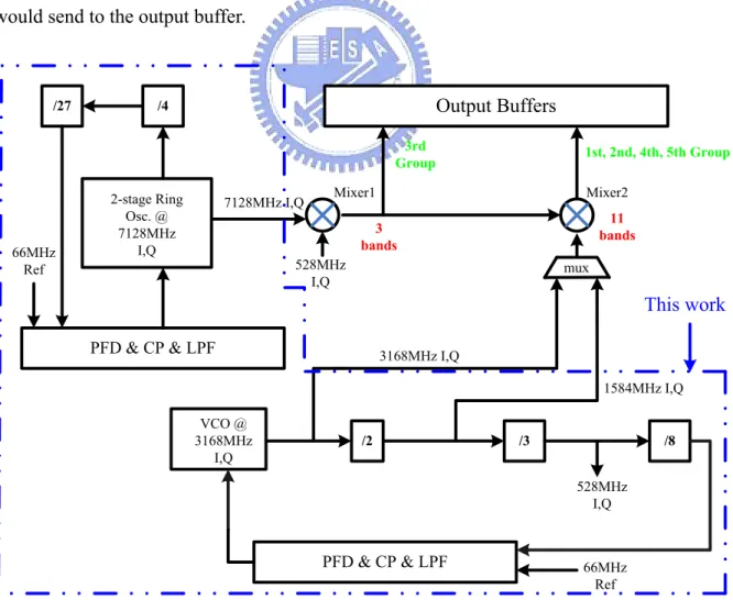
The block diagram of the proposed frequency synthesizer is shown in fig 2.8, which consists of two I/Q output PLLs, two SSB mixers, a multiplexer, and a combined output buffer. It generates the fundamental band (7128 MHz) by the ring oscillator of the first PLL and the input reference frequency is 66 MHz produced by a crystal oscillator with low phase noise distortion. In order to cover the frequency spectrum of Group 3rd in UWB application, the spacing frequency 528 MHz is generated by the cascaded dividers (included a quadrature divider-by-3). The frequency spectrum of Group 3rd (included 6600 MHz, 7128 MHz, and 7656 MHz) would come into existence by the first SSB mixer1. The output of the Group 3rd would send to the output buffer.
528MHz I,Q Mixer1 3rd Group Mixer2 mux VCO @ 3168MHz I,Q /2 /3 /8 PFD & CP & LPF 66MHz Ref 3 bands 528MHz I,Q Output Buffers 3168MHz I,Q 1584MHz I,Q 11 bands 1st, 2nd, 4th, 5th Group 2-stage Ring Osc. @ 7128MHz I,Q PFD & CP & LPF /4 /27 This work 7128MHz I,Q 66MHz Ref
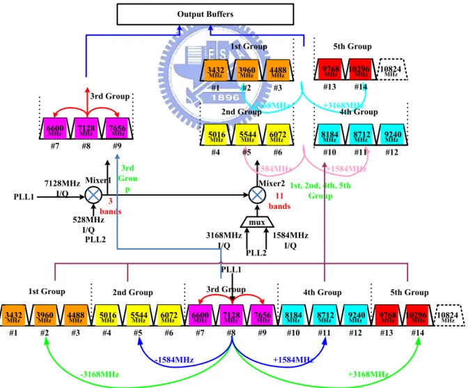
The other frequency spectrum of Group 1st, 2nd, 4th, and 5th are produced at the output of the second SSB mixer2. The extending frequency of 1584 MHz and 3168 MHz are generated by the VCO’s output and the connected divider-by-2. Through the LO signal of the 1584MHz or 3168 MHz, the frequency spectrum of the Group 2nd, 4th or Group 1st, 5th would come into existence at the SSB mixer2. The output of SSB mixer2 would also send to the output buffer, and it would be combined with the output of SSB mixer1. The unique output should be constructed for an exact and complete frequency synthesizer. Finally, it would be a single output and full-band frequency synthesizer for MB-OFDM UWB application. The frequency spectrum generation scheme as the block diagram would be shown in fig 2.9 below.
528MHz I/Q Mixer1 3rd Grou p Mixer2 mux 3 bands Output Buffers 3168MHz I/Q 1584MHz I/Q 11 bands 1st, 2nd, 4th, 5th Group 7128MHz I/Q 3432 3960 4488 5016 5544 6072 6600 7128 7656 8184 8712 9240 9768 10296
1st Group 2nd Group 3rd Group 4th Group 5th Group
MHz MHz MHz MHz MHz MHz MHz MHz MHz MHz MHz MHz MHz MHz #1 #2 #3 #4 #5 #6 #7 #8 #9 #10 #11 #12 #13 #14 +1584MHz -1584MHz +3168MHz -3168MHz PLL1 10824MHz 6600 7128 7656 3rd Group MHz MHz MHz #7 #8 #9 8184 8712 9240 MHz MHz MHz #10 #12 5016 5544 6072 MHz MHz MHz #4 #6 +1584MHz -1584MHz 3432 3960 4488 1st Group MHz MHz MHz #1 #3 9768 10296 5th Group MHz MHz #13 10824 MHz +3168MHz -3168MHz #2 #14 4th Group 2nd Group #11 #5 PLL1 PLL2 PLL2
2.5 Discussion and Comparison
As we mentioned in chapter 2 section 2, the better frequency planning we used, the less circuit components and system disadvantages are revealed. In the followings, the frequency planning architecture for MB-OFDM UWB applications would be compared with previous works at system level. Each frequency planning architecture has its own logical thinking to improve some of the frequency synthesizer’s performance. However, in order to reach the goal covering the 7.5 GHz frequency spectrum and satisfying the UWB specifications, there must be some cost. How to let the cost down and achieve the same purpose is the great issue for us to pay efforts on it. Table 2.2 is the comparison of the proposed frequency planning architecture with the illustrated works in chapter 1.
Table 2.2 The summary and comparison of the UWB frequency synthesizer characteristics
This work [4] JSSC2006 [5] ISSCC2006 [6] MTT-S [7] ISSCC2008 Architecture extending by SSB mixers extending by SSB mixers extending by SSB mixers extending by SSB mixers extending by SSB mixers Frequency range (GHz) 3.1~10.6 3~8 3.1~10.6 3.1~10.6 3.1~10.6 Numbers of PLL 2 2 2 1 1 Numbers of SSB mixer 2 2 3 3 3 Numbers of MUX 1 3 2 2 2 Particular and complicated circuits 1.quadrature divider-by-3 1. tri-mode divider 2. divider-by-13 3. very wide bandwidth SSB mixer 1.quadrature divider-by-3 1.poly phase filter*4 none
The frequency planning architecture at system level of this work has superior advantages on low spurious response, uncomplicated system design, and saving much more chip area for UWB application. As compared to [4], the SSB of this work does not need to operate in very wide bandwidth (over 5 GHz frequency spectrum), and dividers in [4] is also a difficulty to realize. The architecture of [5] must waste an extra SSB mixer to realize the whole system. That causes not only chip area consumption but the lower spurious response. [6] is realized for the past UWB frequency planning specification, and the chip area of [6] is huge because of its poly phase filters. The I/Q mismatch problem is another issue for [6] because the poly phase filter cannot operate exactly at wide frequency range. The SSB mixer in PLL also might cause extra problem in locking and spurious consideration in [6]. The [7] uses extra SSB mixer causing the issue as [5], but [7] only need one PLL. Although this work has more one PLL, we use two-stage ring oscillator to save the chip area. Without the passive component inductor, the chip area would even be smaller than [7]. Finally, in all the frequency generation schemes, this work is the most directly perceived through the sense, and the system is the most uncomplicated to realized.
Chapter 3
Phase Lock Loop Theory and System Simulation
Among the circuit component of frequency synthesizer, the phase-lock-loop is the major part of it. Synthesizers used in commercial radio receivers are largely based on
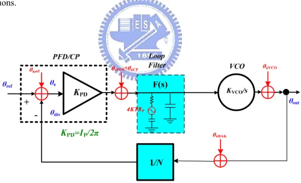
phase-lock-loops ( PLLs). Transceivers’ LO signals are generally produced by it. Because of this, the PLLs play an important role in the radio communications.
Phase-lock-loop (PLL) is a control system that generates a signal that has a fixed relation to the phase of a "reference" signal. A phase-lock-loop circuit responds to both the frequency and the phase of the input signals, automatically raising or lowering the frequency of a controlled oscillator until it is matched to the reference in both frequency and phase. A phase-lock-loop is an example of a control system using negative feedback. It is widely used in radio, telecommunications, computers and other electronic applications. They may generate stable frequencies, recover a signal from a noisy communication channel, or distribute clock timing pulses in digital logic designs such as microprocessors. Since a single integrated circuit can provide a complete phase-lock-loop building block, the technique is widely used in
modern electronic devices, with output frequencies from a fraction of a cycle per second up to many gigahertz. The next section is the general consideration of the PLLs.
3.1 Basic Considerations
Phase Noise
wireless communication systems. Ideally, the output spectrum of a frequency synthesizer should be a pure tone at the desired frequency, as shown in fig 3.1 (a) below. In the time domain, the output can be expressed as:
vout( )t = ⋅A cos(ω0t)
(3-1) However, due to random amplitude and phase fluctuations, the actual output becomes:
[
]
[
]
( ) ( ) cos 0 ( ) out t
v = A+ε t ⋅ ω t+θ t
(3-2) Where ε( )t represents amplitude fluctuations and θ( )t represents phase fluctuations. The actual output spectrum exhibits “skirts” around the desired carrier impulse in the frequency domain, as shown in fig 3.1 (b) below. Because the amplitude fluctuations can be removed or greatly reduced by a limiter, the phase fluctuations, expressed in terms of phase noise, become a bigger and dominant concern in frequency synthesizer design. The phase fluctuations could be attributed to either the external noise at the frequency-tuning input of the oscillator or the noise sources such as thermal, shot, or flicker noise of the devices in the oscillator.
(a) (b)
Figure 3.1 The (a) ideal, (b) actual output spectrum of an oscillator
The phase noise limits the quality of the synthesized signal. In order to quantify the phase noise, the total noise power within a unit bandwidth at an offset frequency (Δω) from the carrier frequency (ω0) is compared with the carrier power. As shown in fig 3.1 (b) above,
this quantity is defined as:
{ }
10 log sideband( 0 ,1 ) carrier P Hz L P ω ω ω ⎡ + Δ ⎤ Δ = ⋅ ⎢ ⎥ ⎣ ⎦ (dBc / Hz) (3-3) Where Psideband(ω0+ Δω,1Hz) represents the single sideband noise power within a 1Hz bandwidth at an offset frequency (Δω).Fig 3.2 below illustrates the impact of the oscillator or synthesizer phase noise in both the receive path and transmit path of a transceiver. As depicted in fig 3.2 (a), in the receive path, the weak desired signal is accompanied by a larger interferer in the adjacent channel. Ideally, the received RF signal is down-converted with a pure LO signal into the desired pure IF signal and the down-converted interferer can be easily filtered. However, in fact, there exists a phase noise skirt around the LO signal. After down-conversion, the weak desired signal could be corrupted by the tail of the interferer spectra and even possibly canceled if the phase noise skirt is too large. It degrades the SNR of the desired signal. In the transmit path, the weak nearby signal of interest can be corrupted by the tail of the large-power transmitted signal, as shown in fig 3.2 (b).
(a) (b)
Therefore, the output spectrum of the LO or synthesizer must be extremely sharp, and a set of stringent phase noise requirements must be achieved so as to satisfy the maximum blocking signal power specified in the wireless communication system.
Settling Time
Transient behavior of the frequency synthesizers is also a critical performance parameter. A change in the division ratio of divider or in the reference frequency would result in a loop transient. Every time a different division ratio or reference frequency is set for channel selection, the synthesizer requires a finite time to lock to the new frequency. The synthesizer needs settling to certain accuracy within the specification of the wireless standard and the overall required time is called “settling time” (also called “locking time”). Also, one thing worth mentioning is that the locking speed requirement of synthesizers is even more stringent for a fast frequency-hopping spread-spectrum system. However, in the UWB specifications, the switching time to the other frequency bands is only 9.47 ns, it is impossible for PLL to lock in such a tiny time. Therefore, changing the frequency bands by settling time of one PLL is not a solution for UWB application. The detailed analysis to model the loop settling behavior will also be discussed in later sections.
Tuning Range
The basic requirement set for a frequency synthesizer by any wireless communication system is that the synthesizer must be able to generate all required frequencies of the system with a sufficient accuracy for channel selection. Therefore, the voltage-controlled oscillator (VCO) and the prescaler must be carefully designed so as to cover the required dynamic frequency range of the synthesizer. However, in our frequency planning architecture, the output frequency of the PLLs should be fixed and unique. This is because of the settling time
of PLL cannot satisfy the UWB specifications (9.47ns).
Spurious Response
Apart from the phase noise, the other key parameter affecting the purity of spectrum synthesized output signal is the relatively high-energy spurious tones (also called spurs), appearing as spikes above the noise skirt, as shown in fig 3.3 (a) below.
Figure 3.3 The (a) spurs, (b) effect of spurs in receive path
Any systematic disturbance on the tuning input of the oscillator will cause the periodic phase variation and thus modulate the synthesized output. In the frequency domain, it manifests itself as the undesired tones at the upper and lower sideband of the carrier. These tones can be quantified by the difference between the carrier power and the spurious power at certain frequency offset in the dBc unit. As illustrated in fig 3.3 (b), similar to the case of phase noise, if a large interferer is close to the weak desired signal and the LO signal has spurs, then both the desired signal and interferer will be mixed down to the IF. If the spacing between the desired signal and the interferer is equal to that between the LO signal and the spur, the spur in the down-converted interferer falls into the center frequency of the desired down-converted signal, and then also degrades the SNR performance. The most common type
![Figure 1.3 The block diagram of the [4]’s full-band frequency planning](https://thumb-ap.123doks.com/thumbv2/9libinfo/8225750.170733/20.892.147.802.519.910/figure-block-diagram-s-band-frequency-planning.webp)
![Figure 1.8 The block diagram of the [7]’s full-band frequency planning](https://thumb-ap.123doks.com/thumbv2/9libinfo/8225750.170733/26.892.127.800.544.747/figure-block-diagram-s-band-frequency-planning.webp)