國 立 交 通 大 學
電子工程學系 電子研究所
碩 士 論 文
積體電路元件充電模式
積體電路元件充電模式
積體電路元件充電模式
積體電路元件充電模式之
之
之
之靜電
靜電
靜電
靜電放電
放電
放電防護設計
放電
防護設計
防護設計
防護設計
Protection Design against
Charged-Device-Model ESD Events in CMOS
Integrated Circuits
研 究 生:張 堂 龍 (Tang-Long Chang)
積體電路元件充電模式
積體電路元件充電模式
積體電路元件充電模式
積體電路元件充電模式之
之
之
之靜電
靜電
靜電
靜電放電
放電
放電防護設計
放電
防護設計
防護設計
防護設計
Protection Design against
Charged-Device-Model ESD Events in CMOS
Integrated Circuits
研 究 生:張堂龍
Student: Tang-Long Chang
指導教授:柯明道教授
Advisor: Prof. Ming-Dou Ker
國立交通大學
電子工程學系
電子研究所
碩士論文
A Thesis
Submitted to Department of Electronics Engineering
and Institute of Electronics
College of Electrical and Computer Engineering
National Chiao-Tung University
in Partial Fulfillment of the Requirements
for the Degree of
Master
in
Electronics Engineering
September 2010
Hsin-Chu, Taiwan
中華民國九十九年九月
積體電路元件充電模式
積體電路元件充電模式
積體電路元件充電模式
積體電路元件充電模式之
之
之
之靜電
靜電
靜電
靜電放電
放電
放電防護設計
放電
防護設計
防護設計
防護設計
研究生 研究生 研究生 研究生::張堂龍::張堂龍張堂龍張堂龍 指導教授指導教授:指導教授指導教授:::柯明道柯明道柯明道 柯明道 博士博士博士 博士 國立交通大學 國立交通大學 國立交通大學 國立交通大學 電子工程學系電子工程學系電子工程學系電子工程學系電子研究所電子研究所電子研究所電子研究所碩士班碩士班碩士班 碩士班Abstract (Chinese)
在奈米 CMOS 製程裡,積體電路的電晶體必須使用很薄的閘極氧化層去達成 高速並且低耗電的效能。但是靜電放電(electrostatic discharge, ESD)的問題不會 隨著奈米 CMOS 元件變小而減弱,所以在奈米 CMOS 製程下的靜電放電防護設 計是更加艱難的。在人體放電模式(human-body model, HBM)、機器放電模式 (machine model, MM)、和元件充電模式(charged-device model, CDM)三種靜電放 電的測試標準裡,元件充電模式靜電放電對積體電路的衝擊更為嚴重。元件充 電 模式之靜電放電是由於積體電路產品因磨擦、移動、或其他因素而在晶片內部累 積了靜電電荷,當某個接腳瞬間接地,靜電電荷便會經由此接腳自晶片內部流出 來。由於系統單晶片的發展趨勢下,晶片尺寸越來越大,而累積在晶片的靜電電 荷也越來越多,在使得積體電路更容易遭受元件充電模式之靜電放電破壞。 在本論文裡,第一部份的研究主題探討當一個輸入端的接腳接地而發生元件充 電模式的靜電放電事件時,經由電感耦合(inductive coupling)的方式而造成內部 電路的電晶體損壞。第二部份的研究主題是針對積體電路內部的電晶體在不同的 防護設計條件之下,檢驗其對元件充電模式靜電放電之耐受能力。
Protection Design against Charged-Device-Model ESD
Events in CMOS Integrated Circuits
Student: Tang-Long Chang Advisor: Dr. Ming-Dou Ker
Department of Electronics Engineering & Institute of Electronics
College of Electrical and Computer Engineering
National Chiao-Tung University
Abstract (English)
With the nanoscale of CMOS processes, the devices in the integrated circuits (ICs) have been fabricated with very thin gate oxide to achieve high-speed and low- power consumption. But, electrostatic discharge (ESD) events were not scaled down with nanoscale CMOS technology. Thus, it becomes a challenging task of ESD protection design in nanoscale CMOS processes. Among the three component-level ESD test standards, therefore are human-body model (HBM), machine model (MM), and charged-device model (CDM), CDM event becomes very critical because of the very thin gate oxide in nanoscale CMOS transistors and the larger die size for the application of system on chip (SoC). The very thin gate oxide causes a very low gate oxide breakdown voltage, which the MOS transistor become more vulnerable to ESD. More static charges can store in the larger die size in an IC of SoC application, which lead to larger discharging current during CDM ESD event. CDM ESD current has features of short duration of few nano-seconds and huge peak current of several. Therefore, effective on-chip ESD protection design against CDM ESD stresses has become more challenging to IC designers.
Some ESD protection designs against CDM ESD events have been presented to
I/O buffers, the core circuits also suffered the dangers as the CDM events happened at
the I/O buffers and coupled to core circuits. In this work, the CDM ESD robustness of
core circuits with coupling effects was investigated in a 65-nm CMOS process.
Besides, the protection design for internal MOS transistor is also important during
the CDM event. In this thesis, the CDM ESD protection devices with different layout
conditions have also been investigated in a 65-nm CMOS process. The experimental
A
CKNOWLEDGMENTS
誌謝
誌謝
誌謝
誌謝
這兩年的碩士生涯裡,雖然不菸也不酒,但倒是交了不少的好朋友,從學長 到學弟,學姊到學妹,不論是學業上還是生活中,都是一起奮鬥打拼的好夥伴。 首先感謝我的指導教授柯明道老師,在這兩年內,雖然身兼多職的老師留在交大 的時間並不長,但每次的meeting中,儘管時間再晚、老師再累,都仍舊仔細聆 聽我們的報告與個人檢討,並精確地指導我們的研究方向與建議。同時老師不在 學校的時候,每次電子郵件的叮嚀與教誨,都讓我獲益良多。再來感謝我最尊敬 的大哥林群祐,你春風化雨兩年來的建議,半夜陪我改layout和PowerPoint,不 知救了我幾次,不時搞笑的風格,以及許許多多研究上的協助,都讓我感動萬分, 不知何以為報。 而這兩年的生活中,感謝文結,書進,逹輸等朋友的陪伴,讓我有了健壯的 體魄,吃到飽的飯友,游泳跑步重訓幹架玩樂打球的好隊友,增重減肥的好夥伴, 感謝各位在課業上的幫忙,你留下的作業會一直流傳下去沒有你我真不知道我這 兩年在幹麻。謝謝阿零哥,你在重訓上的正確指導讓我免於受傷之苦。謝謝阿良 學長,讓我上了一課,一定要打聽好別人住在那才可以先幫你出錢,不然會找不 到人還錢。謝謝達書,吃和,雖然你們很Low又很弱,但你總能給身邊的人帶來 歡樂,讓氣氛永遠也不會僵,到哪都很好玩。謝謝翁姐,總麻煩你團購很多好康 好吃的東西。謝謝佳琪,在苦悶的上課讀書日子裡有你陪聊天。另外感謝小琴、 晚宴、憶如等學弟妹們,在稍晚的meeting中能有你們一起做學術上的討論研究。 同時感謝交通大學,兩年的交大生活讓我與新竹已密不可分,所有的大街小巷或 許已比我高雄家還要熟悉,逛街美食也已成為我生活圈的一大部分。 最後感謝我的父母,沒你們的栽培不會有現在的我,對我的關心與疼愛總是 那麼的無微不至,還有我的姐姐們。 要感謝的人,短短一頁的誌謝裡,永遠也無法說完,想表達的謝意也無法及 意,但和你們一起成長,是我的榮幸,並祝大家萬事如意,快樂平安。 張 堂 龍 僅誌於竹塹交大 九 十 九 年 九 月Contents
Abstract (Chinese)
...
iii
Abstract (English)
...
iv
Contents
...
viii
Table Captions
...
xi
Figure Captions
...
xii
Chapter 1 Introduction
...11.1 Motivation...1
1.2 Thesis Organization...1
Chapter 2 CDM ESD Events and Test Methods
...
3
2.1 CDM ESD Events...3
2.1.1 Chip-Level CDM ESD Event...3
2.1.2 Case Study on Chip-Level CDM ESD Damage...5
2.2 CDM ESD Test Methods...9
2.2.1 Socketed CDM (SDM) ESD Test on Test Pins...11
2.2.2 Non-Socketed CDM (FICDM) ESD Test on Test Pins...13
3.1 Background...17
3.2 ESD Protection Design against Couple Effects...18
3.2.1 Protection Strategy with Ground Shield...18
3.2.2Test Circuit Design against Coupling Events...20
3.3 Experimental Results and Failure Analysis...21
3.3.1 CDM ESD Robustness...21
3.3.2 Failure Analysis...27
3.4 Summary...32
Chapter 4 Investigation on CDM ESD Robustness of
Internal MOS Transistors with CDM Clamp 33
4.1 Background...334.2 Protection Device of CDM Clamp...34
4.2.1 GDPMOS of CDM Clamp Device...34
4.2.2 GGNMOS of CDM Clamp Device...37
4.3 CDM Clamp with Assistance of RCDM...40
4.3.1 GDPMOS with Assistance of RCDM...40
4.3.2 GGNMOS with Assistance of RCDM...43
4.4 Experimental Results...46
4.4.1 CDM ESD Robustness of Deep N-Well...46
4.4.2 Protected Device with Pick-Up / Guard-Ring...57
4.4.3 Failure Analysis...66
4.5 Summary...70
5.1 Conclusion...71
5.2 Future Work...71
References
...
73
VITA
...
75
Table Captions
Table 3.1 CDM ESD robustness of test circuit without inserting shielding...25 Table 3.2 CDM ESD robustness of test circuit with inserting shielding. . 25 Table 4.1 The device size and CDM level of the GDPMOS without deep N-well (DNW) and the GDPMOS with deep N-well (DNW). 35 Table 4.2 The device size and CDM level of the GGNMOS without deep
N-well (DNW) and the GGPMOS with deep N-well (DNW). 38 Table 4.3 The positive CDM level and negative CDM level of the
different p-type device with poly resistor, metal line, and DNW. 56 Table 4.4 The positive CDM level and negative CDM level of the
different n-type device with poly resistor, metal line, and DNW. 56 Table 4.5 The positive CDM level and negative CDM level of the
different p-type device with poly resistor, metal line, and
pick-up. ... 65 Table 4.6 The positive CDM level and negative CDM level of the
different n-type device with poly resistor, metal line, and
Figure Captions
Fig. 2.1 Chip-level CDM ESD events: the stored static charges in the IC product will be quickly discharged, when a certain pin is
grounded. 5 Fig. 2.2 (a) Discharge current path of the CDM event in an input buffer.
(b) The failure point is located at the gate oxide of the input NMOS. ... 6 Fig. 2.3 (a) CDM ESD current path in an output buffer. (b) The diagram
of cross-section view in an output buffer. (c) After chip-level CDM ESD test, the failure point is located at the gate oxide of an output buffer...8 Fig. 2.4 Two type CDM ESD tester: (a) socketed CDM and (b)
non-socketed CDM...10 Fig.2.5 Pin combination in socketed CDM ESD test (a) positive-mode
and (b) negative-mode...12 Fig. 2.6 Pin combination in non-socketed CDM ESD test: (a)
positive-mode and (b) negative-mode. ...14
Fig. 2.7 The non-socket CDM tester.………...………….. …...15
Fig. 2.8 The non-socketed CDM (FICDM) tester ( Oyrx CDM Orion)...16
Fig. 3.1 Propagation of an ESD-CDM event on an IO pin to break down a core transistor gate through inductive coupling.. ...17 Fig. 3.2 (a) The bottom shielding was inserted between I/O traces and the
core traces. (b) The side shielding was inserted beside the I/O traces...19 Fig. 3.3 Diagram of the test circuit with couple events...20 Fig. 3.4 Layout top view of the test circuit with coupled events.. ...21
Fig. 3.6 Comparison among (a) positive CDM level and (b) negative CDM level of the core circuit...26 Fig. 3.7 SEM photo of I/O buffer in 65-nm CMOS process after +200V
CDM ESD testing...28 Fig. 3.8 SEM photo of test circuit A with ground shield structure in
65-nm CMOS process after +200V CDM ESD testing...29 Fig. 3.9 SEM photo of test circuit B with ground shield structure in
65-nm CMOS process after +200 CDM ESD testing.. ...30 Fig. 3.10 (a) Failure mechanism of core circuit. (b) Discharge path under
positive CDM test. (c) Discharge path under negative CDM test...31 Fig. 4.1 When CDM ESD event occurs, accumulated charge in body
cause a large electrical field on gate oxide of the internal circuit.33 Fig. 4.2 (a) GDPMOS without deep N-well (DNW). (b) GDPMOS with
deep N-well (DNW).. ...36 Fig. 4.3 (a) Positive CDM robustness of GDPMOS with and without
deep N-well. (b) Negative CDM robustness of GDPMOS with and without deep N-well...36 Fig. 4.4 (a) GGNMOS without deep N-well (DNW) of CDM clamp. (b)
GGNMOS with deep N-well (DNW) of CDM clamp...39
Fig. 4.5 (a) Positive CDM performance of GGNMOS with and without deep N-Well. (b) Negative CDM performance of GGNMOS with and without deep N-well...39 Fig. 4.6 (a) GDPMOS and protected device not in deep N-well. (b)
Protected device in deep N-Well. (C) GDPMOS in deep N-well...41 Fig. 4.7 N-type protected device with body terminal realized with (a)
four pick-ups at the corner and (b) one guard-ring.. ...42 Fig. 4.8 (a) GGNMOS and protected device without deep N-Well. (b)
Protected device with deep N-well. (C) GGNMOS with deep N-well...44
Fig. 4.9 N-type protected device with body terminal realized with (a) four pick-ups at the corner and (b) one guard-ring...45 Fig. 4.10 Layout top view of the test circuits...46 Fig. 4.11 Comparison among (a) positive CDM level and (b) negative
CDM level of the different p-type device with metal line and DNW...52 Fig. 4.12 Comparison among (a) positive CDM level and (b) negative
CDM level of the different p-type device with poly resistor and DNW...53 Fig. 4.13 Comparison among (a) positive CDM level and (b) negative
CDM level of the different n-type device with metal line and DNW...54 Fig. 4.14 Comparison among (a) positive CDM level and (b) negative
CDM level of the different n-type device with poly resistor and DNW.. ...55 Fig. 4.15 Comparison among (a) positive CDM level and (b) negative
CDM level of the different p-type device with metal line and N+ pick-up.. ...61 Fig. 4.16 Comparison among (a) positive CDM level and (b) negative
CDM level of the different p-type device with poly resistor and N+ pick-up.. ...62 Fig. 4.17 Comparison among (a) positive CDM level and (b) negative
CDM level of the different n-type device with metal line and P+ pick-up... ...63 Fig. 4.18 Comparison among (a) positive CDM level and (b) negative
CDM level of the different n-type device with poly resistor and P+ pick-up...64 Fig. 4.19 The SEM photo of protected device with GGNMOS in DNW
Fig. 4.21 The SEM photo of protected device with GDPMOS after +500V CDM ESD testing. 69
Fig. 4.22 The SEM photo of protected device with GDPMOS after -600V CDM ESD testing. 69
Chapter 1
Introduction
━━━━━━━━━━━━━━━━━━━━━━━━━━━━━━━━━━
1.1 Motivation
Integrated circuits (ICs) have been fabricated with thinner gate oxides to achieve
higher speed and lower power consumption in the advance of CMOS processes.
However, electrostatic discharge (ESD) was not scaled down with CMOS technology.
Among the three chip-level ESD test standards, which are human body model (HBM),
machine model (MM), and charged device model (CDM), CDM becomes more and
more critical because of the thinner gate oxide in nanoscale CMOS transistors and the
larger die size for the application of system on chip (SoC). The electrostatic charges
could be stored within the body of IC products due to induction or tribocharging.
Once a certain pin of the IC is suddenly grounded, the electrostatic charges originally
stored within the IC will be discharged through the grounded pin, which is called as
the CDM ESD event.
1.2 Thesis Organization
To improve the performance of CDM ESD protection devices, two designs
against the CDM event are proposed and discussed in this thesis. This thesis contains
five chapters. The chapter 2 introduces the background of ESD event and the
chip-level CDM event and board-level CDM event. Then, the mechanism that results
in CDM discharge phenomenon of internal transistors is illustrated. In the chapter 3,
verified in a 65-nm CMOS process. The measurement setup and experimental results
including the dc characteristics, field induce CDM test and ESD robustness are stated
in detail in the chapter 3. In the chapter 4, by compared the CDM performance of the
protection device to protect the internal transistor with different metal line length,
resistance, deep N-well (DNW) and pick-up splits, the test is fabricated and verified
in a 65-nm CMOS process. The design concept of test device structure is illustrated
and then the measurement results including field induce CDM test, and ESD
robustness are stated in detail. In the end of this thesis, the conclusion and the future
Chapter 2
CDM ESD Events and Test Methods
━━━━━━━━━━━━━━━━━━━━━━━━━━━━━━━━━━
2.1 CDM ESD Events in CMOS IC
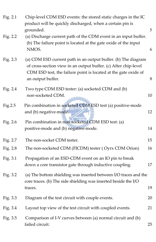
2.1.1 Introduction of Chip-Level CDM ESD Events
During the assemblage of the IC chips, charges could be stored in the substrate of
IC chips due to tribocharging or induction. It is suddenly grounded of the IC chip for
once a certain pin, they originally stored in the IC chips will be discharged through
the grounded certain pin from the static charges, which is called as the CDM ESD
events and shown in Fig.2.1. It delivers a larger of the current in a very short time
form the CDM ESD event. The pin of the IC chips is grounded that have many
situations. For example, the pin may touch grounded by different metallic site. There
are different die sizes of the different IC chips, so they are totally different of their
equivalent substrate parasitic capacitances (Cs) form one another. Thus, there are
different discharge currents and different CDM ESD performances from the different
IC chips. When a device under test (DUT) with a equivalent capacitance of 4pf is
under 1-kV CDM ESD test, it rises to more than 15A within several nanoseconds of
the CDM ESD discharge current [1]. The discharging current in the CDM ESD events
is not only larger, but also faster as compared by HBM and MM ESD events. They
may be damaged during CDM ESD events before the ESD protection circuit is turned
on of the internal circuits, since the duration of CDM ESD event is much shorter than
oxide is most likely to be damaged during CDM ESD events. In the nanoscale CMOS
processes, it becomes very thin of the gate oxide, which increases the equivalent
capacitance per unit area. Therefore, the gate oxides of MOSFET transistors are more
vulnerable to CDM ESD stresses in nanoscale CMOS processes [2-6]. Moreover,
many functions are integrated into one IC chip in system on chip applications, which
increases the die capacitance through it increased the die size. The larger capacitance
stores more static chares under the same charged voltage, so it is larger with larger
capacitance of DUT from the CDM ESD current. The larger equivalent capacitance
since the larger die size, for ICs with larger die sizes the CDM ESD current is larger.
The thinner gate oxide was used by MOSFET transistors with the larger die size, they
are very vulnerable to CDM ESD events in the nanoscale CMOS ICs.
Some of the different steps had been reported to cause chip-level CDM events,
which leads to yield loss during the manufacturing of IC chips. During the
manufacturing of IC products, they have several works addressing the cause of
chip-level CDM ESD events.
When separating the dies and tapes after cutting the dies from wafer, it causes
substantial charge store in the die during fabrication of ICs. To measured by the
Faraday cup, the separation of the dies and tapes had been reported that the CDM
ESD levels could be more than 1000 V. Such it may damage the IC products from a
high CDM ESD voltage [7].
The chips are induced to store charges when the machines are carried by the carrier
in the plastic-leaded-chip-carrier packages. When anyone pin of the charged chip is
connected to ground, when CDM ESD events may occur, to solve this problem, it can
be utilized of the balanced ionizer in the environment of manufacturing to neutralize it
Fig.2.1 Chip-level CDM ESD events: the stored static charges in the IC product will be quickly discharged, when a certain pin is grounded.
2.1.2. Case Study on Chip-Level CDM ESD Damage
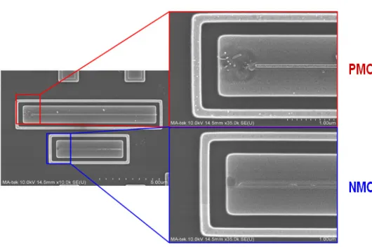
An input buffer fabricated in a 0.8-µm CMOS process is shown in Fig. 2.3(a).
Although the chip is equipped with ESD protection circuit at the input pad, it is still
damaged after 1000-V CDM ESD test. As shown in Fig. 2.3(b), the failure point after
CDM ESD test is located at the gate oxide of the NMOS in the input buffer. Duo to
consideration of noise isolation between I/O cells and internal circuits, the VSS of I/O
cells (VSS_I/O) and the VSS of internal circuits (VSS_Internal) are separated in the
chip layout. As a result, the ESD clamp device at the input pad can not efficiently
protect the gate oxide during CDM ESD stresses, because there is no connection
(a)
(b)
Fig. 2.2 (a) Discharge current path of the CDM event in an input buffer. (b) The
Fig. 2.3(a) is shown an output buffer fabricated in a 0.5-µm CMOS process. After
100V CDM ESD test, this chip is damaged. As shown in Fig.2.3(c), the failure picture
inspected by scanning electron microscopy (SEM). The picture of SEM has proved
that the damage caused by CDM ESD event is located at gate oxide of the NMOS
that is connect to the output pad in the internal circuit. It damaged the gate oxide of
NMOS () from the CDM ESD current is shown by dash line in an output buffer circuit
and the cross-section view in Fig. 2.3(a) and (b), respectively [8].
(b)
(c)
Fig.2.3 (a) CDM ESD current path in an output buffer. (b) The diagram of cross-section
view in an output buffer. (c) After chip-level CDM ESD test, the failure point is located
2.2 Chip-Level CDM ESD Test Methods [9], [10]
Fig. 2.4(a) and Fig. 2.4(b) show the CDM ESD test methods of socketed and
non-socketed CDM (Field-Induce CDM), respectively. In the socketed CDM ESD test,
the test chip in the socket on the test fixture board, the CDM voltage is added into the
pin which is connected to the VSS and stored in the substrate. Once a test pin of the
chip is grounded, the CDM charge stored within the chip will be discharged through the
test pin during the CDM test. The test charge is stored in the distributive network of the
parasitic capacitances and the inductance elements starting from the CDM voltage
supply, the CDM voltage relays, the VSS in the chip, the test pins, and the discharge
relay. The discharge currents through the pin under test represent the charge stored in
the VSS of the chip and socketed CDM test simulators distributive network [9], [10].
In the non-socketed CDM ESD test, two different methods can be used to raise the
component potential for the CDM discharge. Two methods are direct-charging method
and filed-induced method. Since the field-induced method is more realistic than
direct-charging method, so the CDM related experiments are tested by field-induced
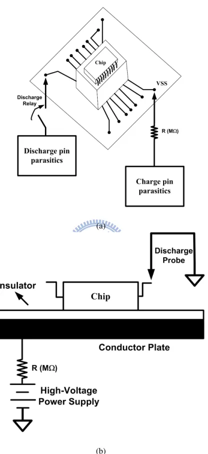
method in this experiments. With the field-induced CDM ESD test, the test chips were
putted on the charging plate. The charge in the chip was induced by the CDM voltage.
Discharge through all test pins, Including power pins and ground pins, without the same
(a)
(b)
2.2.1 Socketed CDM (SDM) ESD Test on Test Pins
Since electrical charges in natural environment can be either positive or negative,
CDM ESD tests have positive and negative modes, too. Moreover, since the CDM ESD
events can occur on input/output (I/O) pins, VDD pins, or between different I/O pins of
an IC chip, ESD test methods have pin combinations as follows. For everyone pin of an
IC chip under the charge-device model ESD tests, there are two test modes as illustrated
through Fig. 2-5(a) to 2-5 (b):
(1). Positive-Mode
The positive CDM ESD voltage is added into the pin which is connected to the VSS
and stored the voltage in the substrate.
Positive ESD voltage applied to the tested I/O pin with VSS pins relatively grounded.
VDD pins and all other pins are kept floating during the test, as shown in Fig. 2-5(a).
(2). Negative-Mode
The negative CDM ESD voltage is added into the pin which is connected to the VSS
and stored the voltage in the substrate.
Negative ESD voltage applied to the tested I/O pin with VSS pins relatively
grounded. VDD pins and all other pins are kept floating during the test, as shown in Fig.
(a)
(b)
Fig.2.5 Pin combination in socketed CDM ESD test (a) positive-mode and (b)
2.2.2 Non-Socketed CDM (FICDM) ESD Test on Test Pins
Since electrical charges in natural environment can be either positive or negative,
CDM ESD tests have positive and negative modes, too. Moreover, since the CDM ESD
events can occur on input/output (I/O) pins, VDD pins, or between different I/O pins of
an IC chip, ESD test methods have pin combinations as follows. For everyone pin of an
IC chip under the charge-device model ESD tests, there are two test modes as illustrated
through Fig. 2-6(a) to 2-6 (b):
(1). Positive-Mode
The positive CDM ESD voltage is added into the pin which is induced to the
substrate and stored the voltage in the substrate.
Positive ESD voltage applied to the tested I/O pin with VSS pins relatively grounded.
VDD pins and all other pins are kept floating during the test, as shown in Fig. 2-6(a).
(2). Negative-Mode
The negative CDM ESD voltage is added into the pin which is induced to the
substrate and stored the voltage in the substrate.
Negative ESD voltage applied to the tested I/O pin with VSS pins relatively
grounded. VDD pins and all other pins are kept floating during the test, as shown in Fig.
(a)
(b)
Fig. 2.6 Pin combination in non-socketed CDM ESD test: (a) positive-mode and (b) negative-mode.
2.2.3. Measurement Tester of CDM Test Chip
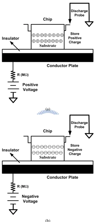
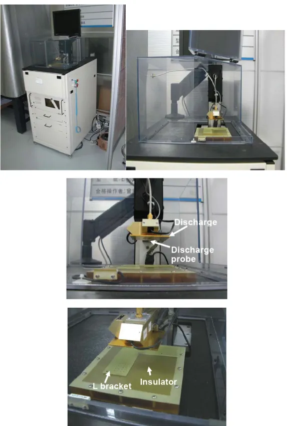
A CDM ESD test system, Oyrx CDM Orion, was used for field-induced chip-level
CDM ESD test. The equipment picture is as Fig. 2.7 shown. The experimental setup of
chip-level CDM ESD tests is shown in Fig. 2.8. In the chip-level CDM ESD test, the
IC chip device under test (DUT) is put on the charging plate of the field-induced CDM
ESD tester. Then set the test pins and discharge to anyone test pins.
Chapter 3
CDM ESD Robustness of Core Circuits with Coupling
Effects
━━━━━━━━━━━━━━━━━━━━━━━━━━━━━━━━━
3.1 Background
The integrated circuit (IC) occur CDM ESD event, when occur at the I/O pin, induce
to break down the core transistor gate with inductive coupling event. The inductive
coupling is the phenomenon that causes the very fast and high-voltage pulse. The pulse
has a pulsewidth of ~100ps.
When the I/O traces occur CDM ESD event that are coupled to core traces, that
causes lead to fail on the thin gate oxide transistors in the core, the induced coupling
voltage on the core traces then the transistor gate oxide to be break down, causing the
transistor function failure, as shown in Fig.3.1.
3.2 ESD Protection Design against Coupling Events
3.2.1. Protection Strategy with Ground Shield [13]
In internal circuit, if a ground shield is near the IO trace, the inductively induced voltage on the core traces can be reduced. During a CDM ESD event, a fast and huge transient current flows in the aggressor IO trace. This current set up the magnetic field, the magnetic field induces a voltage on the core traces. When the ground shield insert, a return current is induced with the ground shield. This direction of the induced current is such that tends to oppose of the induced magnetic field. The result is that less the field of magnetic is available to couple the IO trace to the core traces, the result is reduced induced voltage.
Two different of the ground shields may be implemented with multiple metal layers in the typical technology. If there is available space between the I/O trace and the core traces of one ground shield may be implemented. This is called bottom shielding of this technique. Next one, if there is no available space between the I/O traces and the core traces of the ground shield may be implemented, but it is available on the side of the I/O traces. This is called side shielding of this technique.
(a)
3.2.2. Test Circuit Design against Coupling Events
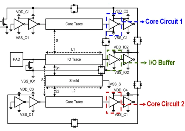
The test circuit is as Fig. 3.4 shown, the input buffer is connected to the input pad with the I/O trace, and the different core circuit is connected with the core trace, the
spacing (S) is between the I/O trace and the core trace, and the length of the I/O trace
and core trace is L1, Another part the spacing (S) is between the I/O trace and the core
trace, and insert the shield between the I/O trace and core trace, the length of the shield
is L2. The lengths of both the I/O trace and the core trace are fixed at 20 µm, 50 µm
and 100µm, and the length L2 of the ground shield varies from 0 µm (where it is
nonexistent) to 20 µm, 50 µm and 100 µm (when it shields the entire length of the core
circuit).
3.3 Experimental Results and Failure Analysis
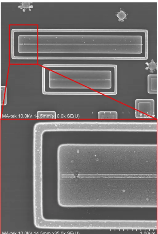
The reference test circuit of couple effect in test circuits with distributed ESD
protection schemes had been fabricated in a 65-nm CMOS process. The chip
micrograph of these fabricated test circuits is shown in Fig. 3.5. In the following
sub-sections, the CDM performances, including positive CDM robustness and negative
CDM robustness of these fabricated test circuits will be measured and compared. The
ESD robustness of these ten test circuits will also be characterized and compared with
failure analysis.
Fig.3.4 Layout top view of the test circuit with coupled events.
3.3.1. CDM ESD Robustness
To compare the ESD robustness, the distributed test circuits five ESD-protected
ground shield of ESD protection only sustains a very low ESD level, which is far
below the ESD specifications for commercial ICs.
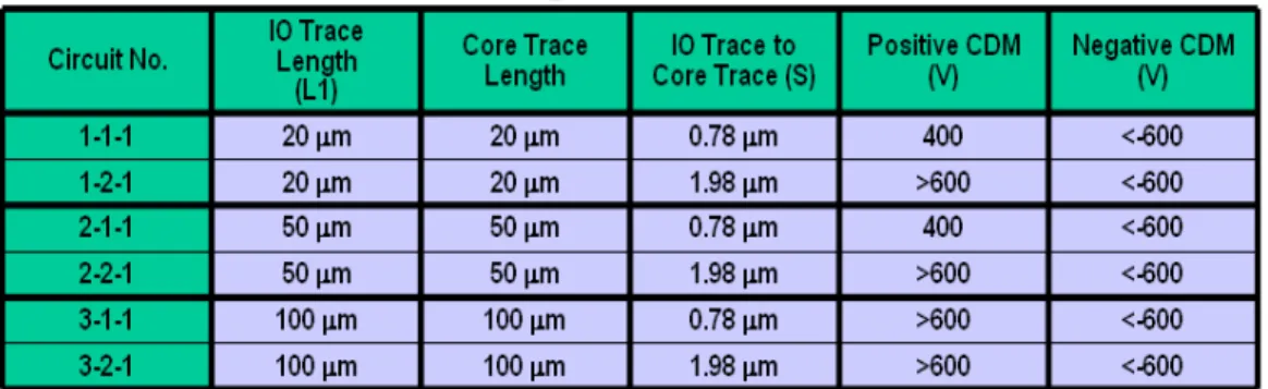
The ESD robustness of the test circuit is not obviously improved after inserting the
ground shield of ESD protection design. The test circuits 1-1 with no insert the ground
shield and spacing is 0.78µm between the I/O trace and core trace of test circuit 1-1-1
has the positive CDM ESD level of 400V and the negative CDM ESD level of more
than -600V, test data is shown in Table 3.1, next one the Length is 20µm of ground
shield and Spacing is 0.3µm between I/O trace and ground shield ESD protection
scheme of test circuit 1-1-2 has the positive CDM ESD level of 100V and the negative
CDM ESD level of <-600V, test data is shown in Table 3.2. The test circuit insert
ground shield is not improved of positive CDM level.
The test circuits 1-2-1 with no insert the ground shield and spacing is 1.98µm
between the I/O trace and core trace of test circuit 1-2-1 has the positive CDM ESD
level of 400V and the negative CDM ESD level of more than -600V, test data is shown
in Table 3.1, next one the Length is 20µm of ground shield and Spacing is 0.9µm
between I/O trace and ground shield ESD protection scheme of test circuit 1-2-2 has
the positive CDM ESD level of 100V and the negative CDM ESD level of <-600V,
test data is shown in Table 3.2. The test circuit insert ground shield is not improved of
positive CDM level.
The test circuits 2-1-1 with no insert the ground shield and spacing is 0.78µm
between the I/O trace and core trace of test circuit 2-1-1 has the positive CDM ESD
level of 400V and the negative CDM ESD level of more than -600V, test data is shown
in Table 3.1, next one the Length is 50µm of ground shield and Spacing is 0.9µm
between I/O trace and ground shield ESD protection scheme of test circuit 2-1-2 has
the positive CDM ESD level of 100V and the negative CDM ESD level of <-600V,
positive CDM level.
The distributed test circuits 2-2-1 with no insert the ground shield and spacing is
1.98µm between the I/O trace and core trace of test circuit 2-2-1 has the positive CDM
ESD level of 400V and the negative CDM ESD level of more than -600V, test data is
shown in Table 3.1, next one the Length is 50µm of ground shield and Spacing is
0.9µm between I/O trace and ground shield ESD protection scheme of test circuit
2-2-2 has the positive CDM ESD level of 100V and the negative CDM ESD level of
<-600V, test data is shown in Table 3.2. The test circuit insert ground shield is not
improved of positive CDM level.
The test circuits 3-1-1 with no insert the ground shield and spacing is 0.78µm
between the I/O trace and core trace of test circuit 3-1-1 has the positive CDM ESD
level of more than 600V and the negative CDM ESD level of more than -600V, test
data is shown in Table 3.1, next one the Length is 100µm of ground shield and Spacing
is 0.9µm between I/O trace and ground shield ESD protection scheme of test circuit
3-1-2 has the positive CDM ESD level of 100V and the negative CDM ESD level of
<-600V, test data is shown in Table 3.2. The test circuit insert ground shield is not
improved of positive CDM level.
The distributed test circuits 3-2-1 with no insert the ground shield and spacing is
1.98µm between the I/O trace and core trace of test circuit 3-2-1 has the positive CDM
ESD level of more than 600V and the negative CDM ESD level of more than -600V,
test data is shown in Table 3.1, next one the Length is 100µm of ground shield and
Spacing is 0.9µm between I/O trace and ground shield ESD protection scheme of test
grounded, the ground shield and I/O trace synthesis parasitic capacitance, the charge
fixed in the substrate where is coupled to I/O trace through the parasitic capacitance.
The charge is caused the current in the ground shield, and the current is inductive
coupled to the core circuit. The CDM ESD robustness is very low through the couple
current. So the distributed circuit with the not inserted the ground shield of protection
scheme exhibits higher CDM ESD robustness than the test circuit with the insert the
ground shield protection scheme.
This measured result has verified that the proposed ground shield protection scheme
can not provide more efficient ESD protection for the test circuits than the not
(a) (b)
Fig. 3.5 Comparison of I-V curves between (a) normal circuit and (b) failed circuit.
Table 3.1 CDM ESD robustness of test circuit without inserting shielding.
(a)
(b)
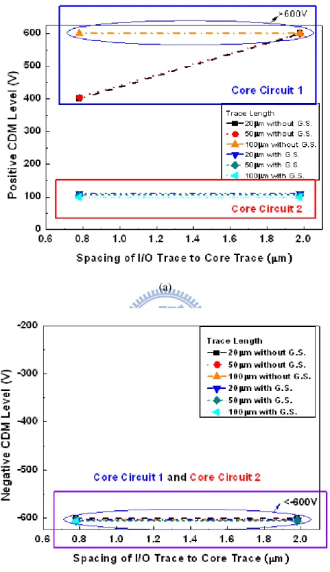
Fig. 3.6 Comparison among (a) positive CDM level and (b) negative CDM level of the core circuit.
3.3.2. Failure Analysis
After the test circuit was damaged by ESD, failure analysis is performed to
investigate the failure mechanism. Fig.3.7 shows the SEM analysis of I/O buffer
inverter circuit in 65-nm CMOS process after field induce CDM testing. The I/O
buffer was damaged at the gate oxide, because the CDM current is very fast and very
large, when I/O pad grounded the CDM current penetrated the gate oxide cause the
gate oxide damage.
Fig. 3.8 show the SEM analysis of test circuit 3-1-2A with insert ground shield
structure and test circuit two with insert ground shield structure after +200V CDM
ESD testing. In the not insert ground shield structure, the position at gate oxide are all
complete, and failure happened because of the couple current by the CDM current on
I/O trace. But in the insert ground shield structure, the gate oxides are all complete, and
failure happened because of the coupled current by the CDM current on ground shield.
Fig. 3.9 show the SEM analysis of test circuit 3-1-2B with insert ground shield
structure and test circuit two with insert ground shield structure after +200V CDM ESD
testing. In the not insert ground shield structure, the position at gate oxide are all
complete, and failure happened because of the couple current by the CDM current on
I/O trace. But in the insert ground shield structure, the gate oxides are all complete, and
failure happened because of the couple current by the CDM current on ground shield.
When the positive CDM charge is fixed in substrate, and the ground shield is
connected in substrate, when I/O pad is grounded, the CDM charge in substrate is
was damaged. Therefore, the CDM performance is deteriorated, shown in Fig. 3.10.
When the negative CDM charge is fixed in substrate, and the ground shield is
connected in substrate, when I/O pad is grounded, the CDM charge in substrate is
coupled to ground by I/O trace and ground shield, through the back-to-back diode and
the GGNMOS to discharge of the charge in substrate, and there is normal discharging
path for the charge in N-well of core circuit 2, the charge in N-well of core circuit 2
must discharges by gate oxide; thus the gate oxide of PMOS in core circuit 2 was
damaged. Therefore, the CDM performance is deteriorated, shown in Fig. 3.10.
Fig. 3.7 SEM photo of I/O buffer in 65-nm CMOS process after +200V CDM ESD
Fig.3.9 SEM photo of test circuit 3-1-2B with ground shield structure in 65-nm CMOS
(a)
3.4. Summary
In this chapter, two kinds circuit of couple effect ESD protection schemes used to
protect the distributed circuit have been reported but not successfully verified in a
65-nm CMOS process. From the experimental results, the circuit of not insert ground
shield, the circuit has coupled effect but CDM level is high, the ESD robustness is
>600V in positive CDM and <-600V in negative CDM, but in the circuit of insert
ground shield can't remove the coupled effect instead the CDM performance is very
low, the ESD robustness is 100V in positive CDM and <-600V in negative CDM.
With the insert ground shield protection scheme can not applied to the distributed
circuit, the ESD robustness is too bad. Therefore, we should be think the other method
to remove the couple effect when CDM occurrence.
The CDM model reported in the paper from Stanford University (T-ED, 2009)
Chapter 4
Investigation on CDM ESD Robustness of Internal
MOS Transistors with CDM clamp
━━━━━━━━━━━━━━━━━━━━━━━━━━━━━━━━━
4.1 Background
When integrated circuit (IC) occur CDM ESD event caused the internal circuit are
damaged. The CDM event often damages the circuits with special layout or design,
and the failure modes for an IC after CDM event include the gate oxide damage,
junction damage and source to drain punch-through. In which the gate oxide damage is
particularly important, because most of the CDM failure sites of the internal circuit is
gate oxide damage. So the internal MOS transistor protection is more important during
the CDM event and shown in Fig.4.1.
In this chapter, in order to investigate what kind structures are sensitive to the CDM
stress, several various structure are designed. And how to improve CDM ESD
4.2 CDM Clamp Devices
4.2.1 Gate-VDD P-Channel MOSFET (GDPMOS) of CDM Clamp
Device
Fig.4.2. (a) and (b) shows the device without deep N-Well (DNW) and device with
deep N-Well (DNW) for gate-vdd p-channel MOSFET (GDPMOS) of CDM clamp
device. Fig.4.3. (a) and (b) shows the positive CDM performance and negative CDM
performance of the GDPMOS without deep N-well (DNW) and the GDPMOS with
deep N-well (DNW).
The positive CDM performance of the GDPMOS with size 180µm /0.09µm and
without deep N-well (DNW) can be achieved 900V, the negative CDM performance of
the GDPMOS with size 180µm /0.09µm and without deep N-well (DNW) can be
achieved -800V. The positive CDM performance of the GDPMOS with size 360µm
/0.09µm and without deep N-well (DNW) can be achieved 1000V, the negative CDM
performance of the GDPMOS with size 360µm /0.09µm and without deep N-well
(DNW) can be achieved -800V. The positive CDM performance of the GDPMOS with
size 540µm /0.09µm and without deep N-well (DNW) can be achieved 1200V, the
negative CDM performance of the GDPMOS with size 540µm /0.09µm and without
deep N-well (DNW) can be achieved -1000V, the test data is shown in Table 4.1.
The positive CDM performance of the GDPMOS with size 180µm /0.09µm and
with deep N-well (DNW) can be achieved 1000V, the negative CDM performance of
the GDPMOS with size 180µm/0.09µm and with deep N-well (DNW) can be achieved
-900V. The positive CDM performance of the GDPMOS with size 360µm /0.09µm
and with deep N-well (DNW) can be achieved 1300V, the negative CDM performance
of the GDPMOS with size 360µm /0.09µm and with deep N-well (DNW) can be
/0.09µm and with deep N-well (DNW) can be achieved 1400V, the negative CDM
performance of the GDPMOS with size 540µm /0.09µm and with deep N-well (DNW)
can be achieved -1200V, the test data is shown in Table 4.1.
Table 4.1 The device size and CDM level of the GDPMOS without deep N-well (DNW) and the GDPMOS with deep N-well (DNW).
(a) (b)
Fig. 4.2 (a) GDPMOS without deep N-well (DNW). (b) GDPMOS with deep N-well (DNW).
(a)
(b)
Fig. 4.3 (a) Positive CDM robustness of GDPMOS with and without deep N-well. (b) Negative CDM robustness of GDPMOS with and without deep N-well.
150 200 250 300 350 400 450 500 550 -1200 -1100 -1000 -900 -800 Width of Device ((((µµµµm)))) N e g a ti v e C D M R o b u s tn e s s ( V ) GDPMOS w/o DNW GDPMOS with DNW 150 200 250 300 350 400 450 500 550 700 800 900 1000 1100 P o s it iv e C D M R o b u s tn e s s ( V ) Width of Device ((((µµµµm)))) GDPMOS w/o DNW GDPMOS with DNW
4.2.2 Gate-Ground N-Channel MOSFET (GGNMOS) of CDM Clamp
Device
Fig.4.4. (a) and (b) shows the device without deep N-well (DNW) and device with
deep N-well (DNW) for gate-ground n-channel MOSFET (GGNMOS) of CDM clamp
device. Fig.4.5. (a) and (b) shows the positive CDM performance and negative CDM
performance of the GGNMOS without deep N-well (DNW) and the GGNMOS with
deep N-well (DNW).
The positive CDM performance of the GGNMOS with size 180µm /0.09µm and
without deep N-well (DNW) can be achieved 900V, the negative CDM performance of
the GGNMOS with size 180µm /0.09µm and without deep N-well (DNW) can be
achieved -800V. The positive CDM performance of the GGNMOS with size 360µm
/0.09µm and without deep N-well (DNW) can be achieved 1000V, the negative CDM
performance of the GGNMOS with size 360µm /0.09µm and without deep N-well
(DNW) can be achieved -800V. The positive CDM performance of the GGNMOS
with size 540µm /0.09µm and without deep N-well (DNW) can be achieved 1200V,
the negative CDM performance of the GGNMOS with size 540µm /0.09µm and
without deep N-well (DNW) can be achieved -1000V, the test data is shown in Table
4.2.
The positive CDM performance of the GGNMOS with size 180µm /0.09µm and
with deep N-well (DNW) can be achieved 1000V, the negative CDM performance of
the GGNMOS with size 180µm /0.09µm and with deep N-well (DNW) can be
achieved -900V. The positive CDM performance of the GGNMOS with size 360µm
CDM performance of the GGNMOS with size 540µm /0.09µm and with deep N-well
(DNW) can be achieved -1200V, the test data is shown in Table 4.2.
Table 4.2 The device size and CDM level of the GGNMOS without deep N-well
(a) (b)
Fig.4.4 (a) GGNMOS without deep N-Well (DNW). (b) GGNMOS with deep N-Well (DNW). (a) (b) 150 200 250 300 350 400 450 500 550 -1300 -1200 -1100 -1000 -900 -800 -700 -600 Width of Device ((((µµµµm)))) N e g a ti v e C D M R o b u s tn e s s ( V ) GGNMOS w/o DNW GGNMOS with DNW 150 200 250 300 350 400 450 500 550 800 900 1000 1100 1200 1300 1400 1500 Po s it iv e C D M R o b u s tn e s s ( V) Width of Device ((((µµµµm)))) GGNMOS w/o DNW GGNMOS with DNW
4.3 CDM Clamp with Assistance of R
CDM4.3.1 GDPMOS with Assistance of R
CDMIn this experiment of CDM test, the ESD protection devices are the GDPMOS and
the p-type protected devices fabricated in a 65-nm CMOS process. The p-type
protected devices used to simulate the internal PMOS transistor with the channel width
is 20um, and GDPMOS of CDM clamp are applied with protection the p-type
protected device with silicide blocking (SAB) and channel width is 180um.
The gate terminal of the p-type protected device is connected to the drain with metal
line or a poly resistance of the GDPMOS to emulate the connection of input PMOS
transistor in internal circuit. The source, drain and body terminals of the p-type
protected device and the source and body terminal of the GDPMOS are connected to
bottom pad. The capacitance between the bottom pad and N-Well of the p-type
protected devices in the 48-pin DIP package is very small. The structures with
different deep N-Well (DNW) location and metal interconnect length and the poly
resistance size to test the CDM clamp device’s protection capability.
The GDPMOS is connected a p-type protected device with metal line or a poly
resistance, and N+ guard-ring of the p-type protected device, as shown in Fig.4.6 (a),
the GDPMOS is connected a p-type protected device in deep N-well (DNW) with
metal line or a poly resistance, and N+ guard-ring of the p-type protected device, as
shown in Fig.4.6 (b), the GDPMOS in deep N-well (DNW) is connected a p-type
protected device with metal line or a poly resistance, and N+ guard-ring of the
protected device, as shown in Fig.4.6 (c). There are two different kinds of N+ pick-up
layouts to assess its effect on the CDM performance of the protected device. The N+
pick-up splits include only four pick-ups at the corner and one guard-ring to rotate the
(a)
(b)
(c)
Fig. 4.6 (a) GDPMOS and protected device without deep N-well. (b) GDPMOS in deep N-Well. (C) Protected device in deep N-well.
(a)
(b)
Fig. 4.7 N-type protected device with body terminal realized with (a) four pick-ups at the corner and (b) one guard-ring.
4.3.2 GGNMOS with Assistance of R
CDM[15]
In this experiment of CDM test, the ESD protection devices are the GGNMOS and
the n-type protected devices fabricated in a 65-nm CMOS process. The n-type
protected device used to simulate the internal NMOS transistor with channel width is
20um, and GGNMOS are applied with protection the n-type protected device with
silicide blocking (SAB) and channel width is 180um.
The gate terminal of the n-type protected device is connected to the drain with metal
line or a poly resistance of the GGNMOS to emulate the connection of input NMOS
transistor in internal circuit. The source, drain and body terminals of the n-type
protected device and the source and body terminal of the GGNMOS are connected to
top pad. The equivalent capacitance between the top pad and P-substrate of the n-type
protected device in the 48-pin DIP package is small. The structures with different deep
N-well (DNW) location and metal interconnect length and the poly resistance size to
test the CDM clamp device’s protection capability.
The GGNMOS is connected a n-type protected device with metal line or the poly
resistance, and P+ guard-ring of the n-type protected device, as shown in Fig.4.8 (a),
the GGNMOS is connected a n-type protected device in deep N-well (DNW) with
metal line or the poly resistance, and P+ guard-ring of the protected device, as shown
in Fig.4.8 (b), the GGNMOS in deep N-well (DNW) is connected a protected device
with metal line or the poly resistance, and P+ guard-ring of the protected device, as
shown in Fig4.8 (c).
There are two different kinds of P+ pick-up layouts to assess its effect on the CDM
(a)
(b)
(c)
Fig. 4.8 (a) GGNMOS and protected device without deep N-well. (b) Protected device
(a)
(b)
Fig. 4.9 N-type protected device with body terminal realized with (a) four pick-ups at the corner and (b) one guard-ring.
4.4. Experimental Results
The reference distributed test circuit in ten distributed circuits with distributed ESD
protection schemes had been fabricated in a 65-nm CMOS process. The chip
micrograph of these fabricated distributed circuits is shown in Fig.4.10. In the
following sub-sections, the CDM performances, including positive CDM robustness
and negative CDM robustness of these fabricated test circuits will be measured and
compared. The ESD robustness of these test circuit will also be characterized and
compared with failure analysis.
Fig.4.10 Layout top view of the test circuits.
4.4.1. CDM ESD Robustness of Deep N-Well
In this work, the CDM clamping by test circuit are GDPMOS and GGNMOS with
different variable or different dimensions. The GDPMOS is realized with a p-type
protection device and a PMOS device (W/L) of 180μm/0.09μm, whose gate and
body is connected to Vdd. The GGNMOS is realized with a n-type protection device
Vss. The CDM ESD levels of devices were measured by ZapMaster and the tested
devices were stressed by three continuous ESD zaps at every CDM ESD test level
under non-socketed CDM (field-induce CDM) mode. The failure criterion is 30%
leakage current shift under 1-V VDD bias.
The positive and negative CDM level of the GDPMOS is connected a p-type
protected device with length is 1.5µm of metal line and N+ guard-ring of the p-type
protected device can be achieved 200V and -300V. The positive and negative CDM
level of the GDPMOS is connected a p-type protected device with length is 300µm of
metal line and N+ guard-ring of the n-type protected device can be achieved 400V and
-500V. The positive and negative CDM level of the GDPMOS in deep N-well (DNW)
is connected a n-type protected device with length is 1.5µm of metal line and N+
guard-ring of the p-type protected device can be achieved 100V and -300V. The
positive and negative CDM level of the GDPMOS in deep N-well (DNW) is connected
a p-type protected device with length is 300µm of metal line and N+ guard-ring of the
p-type protected device can be achieved 200V and -500V. The positive and negative
CDM level of the GDPMOS is connected a n-type protected device in deep N-well
(DNW) with length is 1.5µm of metal line and N+ guard-ring of the p-type protected
device can be achieved 100V and -200V. The positive and negative CDM level of the
GDPMOS is connected a p-type protected device in deep N-well (DNW) with length is
300µm of metal line and P+ guard-ring of the p-type protected device can be achieved
200V and -400V.
The positive and negative CDM level of the GDPMOS is connected p-type
400V and -500V. The positive and negative CDM level of the GDPMOS is connected
p-type protected device with resistance is 10kΩ of poly resistor and N+ guard-ring of
the n-type protected device can be achieved 800V and -700V.
The positive and negative CDM level of the GDPMOS is connected p-type
protected device in deep N-well (DNW) with resistance is 0.1kΩ of poly resistor and
N+ guard-ring of the p-type protected device can be achieved 200V and -400V. The
positive and negative CDM level of the GGNMOS is connected p-type protected
device in deep N-well (DNW) with resistance is 1kΩ of poly resistor and N+
guard-ring of the p-type protected device can be achieved 300V and -500V. The
positive and negative CDM level of the GDPMOS is connected p-type protected
device with resistance is 10kΩ of poly resistor and N+ guard-ring of the p-type
protected device can be achieved 800V and -700V.
The positive and negative CDM level of the GDPMOS is connected p-type
protected device with resistance is 0.1kΩ of poly resistor and N+ guard-ring of the
p-type protected device can be achieved 200V and -300V. The positive and negative
CDM level of the GDPMOS is connected p-type protected device with resistance is
1kΩ of poly resistor and N+ guard-ring of the p-type protected device can be achieved
300V and -500V. The positive and negative CDM level of the GDPMOS is connected
n-type protected device with resistance is 10kΩ of poly resistor and N+ guard-ring of
the p-type protected device can be achieved 800V and -700V.
Fig. 4.11 (a) compares the positive CDM level on the different p-type device with
metal line and DNW, as the length of metal line increased, the positive CDM
robustness increased. The different p-type device put in DNW can not remove the
CDM discharge current, it will be even worse of the p-type device put in DNW.
Fig. 4.11 (b) compares the negative CDM level on the different p-type device with
robustness increased. The different p-type device put in DNW can not remove the
CDM discharge current, it will be even worse of the p-type device put in DNW.
Fig. 4.12 (a) compares the positive CDM level on the different p-type device with a
poly resistor and DNW, as the length of metal line increased, the positive CDM
robustness increased. The different p-type device put in DNW can not remove the
CDM discharge current, it will be even worse of the p-type device put in DNW.
Fig. 4.12 (b) compares the negative CDM level on the different p-type device with a
poly resistor and DNW, as the length of metal line increased, the negative CDM
robustness increased. The different p-type device put in DNW can not remove the
CDM discharge current, it will be even worse of the p-type device put in DNW.
Table 4.3 Show the positive CDM level and negative CDM level on the different
p-type device with poly resistor, metal line and DNW.
The positive and negative CDM level of the GGNMOS is connected a n-type
protected device with length is 1.5µm of metal line and P+ guard-ring of the n-type
protected device can be achieved 400V and -200V. The positive and negative CDM
level of the GGNMOS is connected a n-type protected device with length is 300µm of
metal line and P+ guard-ring of the n-type protected device can be achieved 600V and
-500V. The positive and negative CDM level of the GGNMOS in deep N-well (DNW)
is connected a n-type protected device with length is 1.5µm of metal line and P+
guard-ring of the n-type protected device can be achieved 200V and -100V. The
positive and negative CDM level of the GGNMOS in deep N-well (DNW) is
connected a n-type protected device with length is 300µm of metal line and P+
negative CDM level of the GGNMOS is connected a n-type protected device in deep
N-well (DNW) with length is 300µm of metal line and P+ guard-ring of the n-type
protected device can be achieved 700V and -600V.
The positive and negative CDM level of the GGNMOS is connected n-type
protected device with resistance is 0.1kΩ of poly resistor and P+ guard-ring of the
n-type protected device can be achieved 400V and -300V. The positive and negative
CDM level of the GGNMOS is connected n-type protected device with resistance is
1kΩ of poly resistor and P+ guard-ring of the n-type protected device can be achieved
600V and -400V. The positive and negative CDM level of the GGNMOS is connected
n-type protected device with resistance is 10kΩ of poly resistor and P+ guard-ring of
the n-type protected device can be achieved more than 800V and -800V.
The positive and negative CDM level of the GGNMOS is connected n-type
protected device in deep N-well (DNW) with resistance is 0.1kΩ of poly resistor and
P+ guard-ring of the n-type protected device can be achieved 200V and -100V. The
positive and negative CDM level of the GGNMOS is connected n-type protected
device in deep N-well (DNW) with resistance is 1kΩ of poly resistor and P+
guard-ring of the n-type protected device can be achieved 500V and -400V. The
positive and negative CDM level of the GGNMOS is connected n-type protected
device with resistance is 10kΩ of poly resistor and P+ guard-ring of the n-type
protected device can be achieved 800V and -700V.
The positive and negative CDM level of the GGNMOS is connected n-type
protected device with resistance is 0.1kΩ of poly resistor and P+ guard-ring of the
n-type protected device can be achieved 500V and -400V. The positive and negative
CDM level of the GGNMOS is connected n-type protected device with resistance is
1kΩ of poly resistor and P+ guard-ring of the n-type protected device can be achieved
n-type protected device with resistance is 10kΩ of poly resistor and P+ guard-ring of
the n-type protected device can be achieved more than 800V and -800V.
Fig. 4.13 (a) compares the positive CDM level on the different n-type device with
metal line and DNW, as the length of metal line increased, the positive CDM
robustness increased. The different n-type device put in DNW can not remove the
CDM discharge current, it will be even worse of the n-type device put in DNW.
Fig. 4.13 (b) compares the negative CDM level on the different n-type device with
metal line and DNW, as the length of metal line increased, the negative CDM
robustness increased. The different n-type device put in DNW can not remove the
CDM discharge current, it will be even worse of the n-type device put in DNW.
Fig. 4.14 (a) compares the positive CDM level on the different n-type device with a
poly resistor and DNW, as the length of metal line increased, the positive CDM
robustness increased. The different n-type device put in DNW can not remove the
CDM discharge current, it will be even worse of the n-type device put in DNW.
Fig. 4.14 (b) compares the negative CDM level on the different n-type device with a
poly resistor and DNW, as the length of metal line increased, the negative CDM
robustness increased. The different n-type device put in DNW can not remove the
CDM discharge current, it will be even worse of the n-type device put in DNW.
Table 4.4 Show the positive CDM level and negative CDM level on the different
(a)
(b)
Fig.4.11 Comparison among (a) positive CDM level and (b) negative CDM level of the
different p-type device with metal line and DNW.
0
50
100
150
200
250
300
-800
-700
-600
-500
-400
-300
-200
-100
0
Length of Metal Line
((((µ
µ
µ
µ
m
))))N
e
g
a
ti
v
e
C
D
M
R
o
b
u
s
tn
e
s
s
(
V
)
Both Devices w/o DNW
P-Type CDM Clamp with DNW P-Type Protected Device with DNW
0
50
100
150
200
250
300
0
100
200
300
400
500
600
700
800
P
o
s
it
iv
e
C
D
M
R
o
b
u
s
tn
e
s
s
(
V
)
Length of Metal Line
((((µ
µ
µ
µ
m
))))Both Devices w/o DNW
P-Type CDM Clamp with DNW P-Type Protected Device with DNW