國 立 交 通 大 學
電子工程學系 電子研究所碩士班
碩 士 論 文
多重閘極金氧半場效電晶體的本質參數變異特性分析
Investigation of Intrinsic Parameter Fluctuations for
Multi-Gate MOSFETs
研 究 生:范銘隆
指導教授:蘇 彬 教授
多重閘極金氧半場效電晶體的本質參數變異特性分析
Investigation of Intrinsic Parameter Fluctuations for Multi-Gate
MOSFETs
研 究 生:范銘隆 Student: Ming-Long Fan
指導教授:蘇 彬 Advisor: Pin Su
.
國 立 交 通 大 學
電子工程學系 電子研究所
碩 士 論 文
A Thesis
Submitted to Department of Electronics Engineering & Institute of Electronics College of Electrical and Computer Engineering
National Chiao Tung University in Partial Fulfillment of the requirements
for the Degree of Master in
Electronic Engineering September 2008
Hsinchu, Taiwan, Republic of China
多重閘極金氧半場效電晶體的本質參數變異特性分析
研究生:范銘隆 指導教授:蘇 彬
國立交通大學電子工程學系 電子研究所碩士班
摘要
本論文系統化地探討了三種重要的本質參數變異:隨機參雜濃度變動
(Random Dopant Fluctuation)、線邊緣的粗糙程度 (Line Edge Roughness) 以及
等效氧化層厚度變異 (Equivalent Oxide Thickness Variation) 對於多重閘極金氧
半場效電晶體變異特性的影響。更精確地說,我們利用 Atomistic 模擬以及傅立
葉分析探討元件微縮對於多重閘極金氧半場效電晶體變異特性的影響。
經由模擬的結果我們得知:對於高參雜元件而言,隨機參雜濃度變動是最
主要的變異來源。在低參雜的元件方面,我們探討了兩種不同類別的線邊緣粗
操程度。第一個類別是悲觀地假設線邊緣粗操程度並不會隨著元件微縮而得到
相對應的改善;在這個情況下,我們發現線邊緣粗糙程度對於多重閘極電晶體
變異程度的影響將比隨機參雜濃度變動以及等效氧化層厚度變異嚴重。在第二
個類別中,線邊緣粗操程度遵循 ITRS 對於不同世代電晶體理想的預測;我們
發現在高度微縮的元件中,由於局部等效通道長度的變異,源極/汲極隨機參雜
濃度變異的重要性將會逐漸升高。這意味著在低參雜濃度且高度微縮的多重閘
極金氧半場效電晶體,利用 Atomistic 模擬來分析元件的變異特性是必須。
Investigation of Intrinsic Parameter Fluctuations for
Multi-Gate MOSFETs
Student : Ming-Long Fan Advisor : Pin Su
Department of Electronics Engineering
Institute of Electronics
National Chiao Tung University
Abstract
This thesis systematically investigates three important intrinsic parameter
fluctuations, random dopant fluctuation (RDF), line edge roughness (LER) and
equivalent oxide thickness (EOT) variation in multi-gate MOSFETs. Specifically,
we have performed atomistic simulation and Fourier synthesis to investigate the
impact of scaling on the variability of multi-gate devices.
Our results indicate that RDF is the dominant variation source for heavily
doped devices. For lightly doped devices, two scenarios for LER have been
examined. In the pessimistic scenario that the LER does not scale with the
technology generation, we find that the LER will dominate over the RDF and EOT
variation. In the optimistic scenario that the LER follows the ITRS roadmap for each
technology node, the Source/Drain RDF becomes increasingly important in
ultra-small devices because of the local variation of effective channel length. In
other words, the atomistic simulation has to be employed for lightly doped
extremely-scaled multi-gate devices.
誌
誌
誌
誌
謝
謝
謝
謝
碩士論文付印在即,這意味著碩士生涯即將邁入尾聲;回想起這兩年來的點 點滴滴,箇中酸甜苦辣雖無法一一言述,但對於自己曾經走過的路以及身邊曾出 現的人依舊是歷歷在目及心懷感激。 在研究方面,我得感謝我的指導教授蘇彬老師。在這近兩年的研究生涯中, 老師對於研究的熱忱以及實事求是的精神一直是學生學習的榜樣;當中更感謝老 師不辭辛勞地給予學生包容以及在研究方面的諸多建議與鼓勵,讓學生得以在毫 無頭緒時找到一盞明燈。此外,感謝李維學長、吳育昇學長、小郭學長、Vita 學姊、昆諺以及欣原於口試期間給我的幫助以及平日的討論與關心,你們的陪伴 豐富了我這兩年的生活。另外要感謝的是曾俊元老師實驗室的孟翰學長以及明錡 學長,和你們一起運動以及聊天的過程中讓我在這兩年緊湊的生活中獲得不少調 劑以及壓力的舒緩,謝謝你們! 其次,我要感謝交大棒球隊的黃杉楹教練,謝謝你這幾年來的指導與器重, 除了讓我有發揮的舞台之外,更讓我學會了許多做人做事的道理。更感謝棒球隊 的諸多學長們:阿麟、兆平、六千、kemp、岳璋以及 93 級的邱毛、浩呆、老周 以及 Jason、帥詮、俊賓和阿福,謝謝你們這幾年來對我的照顧及關心;同屆的 昱丞、阿宅以及宗佑,很高興這幾年來能跟你們一起同甘共苦,和你們一起相處 過的生活是我最珍惜的回憶。 另外要感謝的是從小到大的玩伴們:建龍、峻誠、歆平、耀成、祥育以及峰 威,謝謝你們有情有義地陪伴我度過人生中的種種酸甜苦辣,有你們真好!最 後,謝謝我的父親范朝鐘先生以及母親羅秀珍女士二十餘年的養育之恩,你們多 年來刻苦耐勞的工作以及為子女們所做的犧牲一直是支持我在困境中站起來的
動力。
“得之於人太多,出之於己太少”,謹以此論文獻給曾經給予我批評、幫助的人 們。
Contents
Abstract (Chinese)………...………..I
Abstract (English)………...…….II
Acknowledgement………...…...……III
Contents………...…………...V
Figure Captions………...VI
Table Captions………...…………XI
Chapter 1 Introduction………...……...…...…………...…...1
1.1 Background...1
1.2 Literature Review and Motivation...2
1.3 Organization...3
Chapter 2 Random Dopant Fluctuation…….…...……...4
2.1 Introduction………...4
2.2 Methodologies………...5
2.2.1 Setting the Scene………...…5
2.2.2 Atomistic Simulation Approaches…….………...7
2.3 Results and Discussions………...…….9
2.4 Modified Atomistic Simulation ………...……..13
2.5 Summary………...15
Chapter 3 Line Edge Roughness and Equivalent Oxide Thickness
Variation………...…...33
3.1.1 Introduction………...………..33
3.1.2 Methodologies………...…………..34
3.1.2.1 Concept………...………..34
3.1.2.2 Simulation Approach……...………...35
3.1.3 Results and Discussions………...36
3.2 Equivalent Oxide Thickness Variation…………...…………39
3.2.1 Introduction………..…...39
3.2.2 Methodologies………....…….…...…….40
3.2.3 Results and Discussions……….…………...42
3.3 Summary………...……43
Chapter 4 Variability in Multi-Gate MOSFETs………...…...61
4.1 Introduction………...61
4.2 Intrinsic Parameter Fluctuations in Multi-Gate MOSFETs...61
4.3 Comparison of Planar and Multi-Gate MOSFETs………...63
4.4 Summary………...64
Chapter 5 Conclusions………...……….…70
References………...72
Figure Captions
Fig. 2.1 Poisson distribution of the dopant number inside the active region. The figure includes 10000 ensembles with 94 mean dopants...16 Fig. 2.2 Top view of 3D random dopant arrangements with 120 dopants inside the region. Closed circles represent dopant atoms. Demonstrated device dimensions are Lg = 100nm, TSOI = 10nm and Wg = 40nm with
doping=3 10× 18cm-3...17 Fig. 2.3 Top view of 3D random dopant arrangements with 4 dopants inside the
region. Closed circles represent dopant atoms. Demonstrated device dimensions are Lg = 100nm, TSOI = 10nm and Wg = 40nm with
doping=1 10× 17cm-3...18 Fig. 2.4 Perspective view and geometry definitions of the multi-gate MOSFET used in this work...19 Fig. 2.5 Example of atomistic dopant placement in the channel region of a multi-gate MOSFET with Lg = 25nm, Wfin = 15nm, Hfin = 30nm. Closed circle symbols
represent dopant atoms...20 Fig. 2.6 Our quasi-uniform meshes used for 3-D RDF device simulations in view of (a)
perspective, (b) S/D and channel, (c) y-z cross-section, (d) x-z cross-section, (e) x-y cross-section...21 Fig. 2.7 Simulation approach for dopant number fluctuation...22 Fig. 2.8 Simulation approach for dopant position fluctuation...22 Fig. 2.9 Potential distribution at Si/SiO2 interface with discrete dopants inside the
channel. Potential distribution is distorted due to discrete dopants and this is the cause of threshold voltage variation...23
Fig. 2.10 Id-Vg curves for conventional simulation (Triangle), 150 atomistic simulations (solid lines) and the average of these atomistic simulations (square)...24 Fig. 2.11 Histogram plots of S/D swapping with 150 microscopically different (a) heavily doped and (b) lightly doped Tri-gate devices. Here forward means before S/D swapping operation and reverse means after S/D swapping...25 Fig. 2.12 Histogram plots of Vth difference between S/D swapping for (a) heavily
doped and (b) lightly doped Tri-gate MOSFETs...26 Fig. 2.13 The correlation coefficients between the normalized threshold voltages and the dopant number are (a) 0.64 for heavily doped and (b) 0.21 for lightly
doped Tri-gate
devices...27 Fig. 2.14 Our full Monte Carlo simulation can capture both number and position fluctuations...28 Fig. 2.15 Dependence of Rposition on different AR multi-gate devices for heavily doped
and lightly doped channels...28 Fig. 2.16 The AR dependence of threshold voltage fluctuations for (a) heavily doped and (b) lightly doped devices...29 Fig. 2.17 Doping dependence of threshold voltage variation for 3 AR devices.
Threshold voltage variations are determined by the electrostatic integrity and doping concentration...30 Fig. 2.18 Threshold voltage variation as a function of the (a) doing concentration NAb
behind the epi-layer and (b) delta-doping dose Qδ for a set of 50×50 nm
MOSFETs with tox = 3nm, NAb = 1×1018 cm-3, NAe = 1×1015 cm-3, at different
epi-layer thickness [28]. Inset plot shoes the definition of epi-layer. (c) shows electrostatic integrity of conditions in (a). DIBL is defined as
|VT(Vd=0.05V)-VT(Vd=1V)|/(1-0.05)...31 Fig. 2.19 (a) 1D representation of long-range and short-range parts of the dopant
number density and (b) 3D perspective view of long-range part number density. Long-range potential does not diverge at the origin...32 Fig. 3.1 Magnitude spectrum of a real LER pattern. It resembles low-pass filter. The
figure is revised from [9]...45 Fig. 3.2 Magnitude spectrum of LER from real line pattern accompanied with the Gaussian and exponential models [10]...45 Fig. 3.3 Example of randomly generated LER using 1D Fourier synthesis with rms amplitude = 2nm and correlation length = 12nm...46 Fig. 3.4 Simulation flow to generate the fin- and gate- LER...46 Fig. 3.5 Rms amplitude dependence of the Gaussian model in (a) absolute magnitude and (b) normalized magnitude and (c) LER pattern...47 Fig. 3.6 Correlation length dependence of the Gaussian model in (a) absolute magnitude and (b) LER pattern...48 Fig. 3.7 Rms amplitude dependence of threshold voltage variation for the (a) fin LER and (b) gate LER...49 Fig. 3.8 Comparison of gate and fin LER of FinFET (AR=2) devices at different
technology nodes. Quantum mechanical correction is applied...49 Fig. 3.9 Correlation length dependence of threshold voltage variation for the (a) fin LER and (b) gate LER. Fin widths are 37.5nm, 25nm and 15nm for AR=0.5, 1, 2 devices, respectively...50 Fig. 3.10 Explanation of Vth fluctuation saturation...51 Fig. 3.11 Comparison of total LER at 1E17 cm-3 and 6E18 cm-3 channel doping. Heavily doped devices show better immunity to LER...51
doping. LER includes both fin and gate components...52 Fig. 3.13 Dopant number inside the channel with (a) no LER (b) LER with rms = 1.5nm and (c) LER with rms = 2.5nm...53 Fig. 3.14 Oxide thickness variation generated by the Fourier synthesis for (a) original rough surface and (b) the digitized surface...54 Fig. 3.15 Demonstration of OTV for multi-gate MOSFETs...55 Fig. 3.16 1D representation of determining high-k non-uniformity with two extreme dielectric constant values...55 Fig. 3.17 Demonstration of (a) the TEM image of HfOSi film [40] and (b) the
simulated pattern. Black colored is SiO2 and white ones are HfO2...56 Fig. 3.18 Dielectric patterns produced with different parameters: (a) Λ=2.5nm, α=0.25
(b) Λ=2.5nm, α=0.75 (c) Λ=10nm, α=0.25 (d) Λ=10nm, α=0.75. Black colored is SiO2 and white ones are HfO2...57 Fig. 3.19 The impacts of channel doping, AR and correlation length on OTV...58 Fig. 3.20 Vth variation induced by OTV at different channel doping...58 Fig. 3.21 Potential distribution of a planar MOSFET. Surface potential is distorted by
the DCF...59 Fig. 3.22 The AR and correlation length dependence of DCF...59 Fig. 3.23 Comparison of RDF, LER and EOT at (a) 6E18 cm-3 and (b) 1E17 cm-3 channel doping. LER and EOT are with correlation length = 10nm...60 Fig. 4.1 Threshold voltage variation for 25-, 18-, 13- and 9-nm channel length MOSFETs due to RDF, LER and EOT variation. LER is kept at rms = 1.5nm and correlation length = 30nm...66 Fig. 4.2 Id-Vg characteristic of 150 9-nm FinFETs due to fin LER...67 Fig. 4.3 AR dependence of gate and fin LER fluctuations for 9-nm FinFETs...67 Fig. 4.4 Threshold voltage variation for 25-, 18-, 13- and 9-nm channel length
MOSFETs due to RDF, LER and EOT. LER follows the ITRS roadmap with correlation length = 30nm...68 Fig. 4.5 Comparison of individual variation source for planar and FinFET devices.
LER is kept at rms = 1.5nm and correlation length = 30nm...69 Fig. 4.6 Comparison of overall Vth fluctuation for planar and FinFET transistors. LER
Table Captions
Table 2.1. Comparison of the atomistic results in this work and [18]...23 Table 2.2. Detailed data of Vth shift and Vth variations for devices with Lg = 25nm and
Wtotal = 75nm. Vth lowering is defined as Vth (atomistic) – Vth
(continuous)...24 Table 4.1 Specifications of model parameters used in the work...66 Table 4.2 Design parameters of planar and multi-gate MOSFETs...68
Chapter 1
Introduction
1.1 Background
For better performance and higher packing density, the dimensions of CMOS devices have shrunk tremendously over the past decades. However, several deviations from the ideal switch characteristic have been found during CMOS scaling. These deviations include drain induced barrier lowering (DIBL), worse subthreshold swing, larger leakage current, and so on [1]. To overcome the difficulty of scaling, multiple-gate device structure has been proposed to enhance the gate controllability over the channel [2]. With better gate control, multi-gate MOSFETs are expected to be one of the most promising candidates for sub-22nm CMOS scaling [3-4].
For devices in the decananometer regime, several atomic-level imperfections such as discreteness of ionized dopant, ragged line edge and interface, and non-uniformity of gate stack materials may become pronounced because of the smaller device critical dimension and doubled number of transistors in a chip for every generation ahead [5-6]. It is expected to severely degrade circuit functionality and yield if we do not pay attention to this problem [7]. Moreover, it is difficult to capture device variability by investigating single device or using conventional simulation approach. Instead, we should collect a large amount of macroscopically identical but microscopically different ensembles and analyze their impacts on device parameters such as threshold voltage, subthreshold swing or leakage current statistically. This is a computation consuming task even with the most powerful
simulation equipments nowadays.
Generally speaking, mismatch can be grouped into intrinsic (stochastic) and extrinsic (systematic) categories. Intrinsic variation refers to the atomic level discrepancy between devices under the same process environment. On the other hand, extrinsic variation is due to the process induced parameter shifts which can be suppressed by further process improvements. It is difficult to mitigate the intrinsic mismatch, which is believed to become an obstacle for future device scaling.
There are several noticeable intrinsic variation sources: Random Dopant Fluctuation (RDF) caused by the sparse number of dopant atoms in the scaled active region [8], Line Edge Roughness (LER) or surface roughness induced by the resolution limits of lithography and etching processes [9-10], and Equivalent Oxide Thickness (EOT) variation from the gate physical thickness and high-k gate materials non-uniformity [11-12]. These fluctuations can be assessed with various methods. In this work, we will employ adequate simulation approaches for these variation mechanisms and investigate their impacts on multi-gate devices.
1.2 Literature Review and Motivation
Although most studies in the past regarding device variations were concentrated on planar devices [5-6], there are more and more researches on the multi-gate variability. For example, A.V-Y Thean et. al. [13] provided experimental data in the comparison of multi-gate FETs and planar SOI transistors. They concluded that un-doped FinFETs suffer smaller variability problem but higher sensitivity to fin
width. F-L Yang et. al. [14] compared planar transistors with non-planar counterparts in the RDF and LER aspects. E. Baravalli et. al. [15] discussed the impact of LER on the FinFET matching performance with a sophisticated method as described in [10]. In [16], Y-S Wu et. al. investigated the sensitivity of multi-gate MOSFETs to process variations with analytical model approach. They found that lightly doped FinFET suffers smallest Vth variation caused by the process variation and dopant number
fluctuation.
However, there is still a need for a comprehensive and systematic examination on the multi-gate device variability. For example, an extensive and detailed consideration of different fluctuation sources as considered in planar transistors [5-6] is required. A comparison of planar and non-planar FETs for various technology nodes is also important. In addition, an assessment of optimum multi-gate device design considering the intrinsic parameter fluctuations is needed. Therefore, in this work, we conduct a comprehensive investigation for intrinsic parameter fluctuations in multi-gate MOSFETs.
1.3 Organization
This thesis is organized as follows. In chapter 2, we investigate the impact of RDF on multi-gate MOSFETs using atomistic simulation. In chapter 3, the effects of LER on multi-gate devices are assessed using Fourier synthesis. Besides, with similar approach, EOT variation is also discussed. In chapter 4, we investigate the intrinsic parameter fluctuations in multi-gate MOSFETs for several technology generations and point out the dominant variation source. Chapter 5 concludes this work.
Chapter 2
Random Dopant Fluctuation
2.1 Introduction
Since 2007, 45nm technology node high-k/metal-gate planar metal oxide semiconductor field effect transistors (MOSFETs) have been in mass production [17]. However, devices become more susceptible to stochastic disturbances. For example, if we assume the device with 20nm 20nm 20nm× × active region and channel doping =6 10 cm× 18 −3, there would be only fifty dopants inside the region. Even with the well-controlled lithographic patterns and etching processes, intrinsic fluctuation of the dopant number and placement in the channel of these highly-scaled MOSFETs will lead to significant dispersion of threshold voltage, current, and so on.
In this chapter, we will investigate random dopant fluctuation by performing 3-D “atomistic” simulation, that is, treating each dopant individually. Random dopant fluctuation can be further classified into number and position components. We will introduce random dopant fluctuation qualitatively in this section, and then quantitatively investigate their characteristics in the following sections.
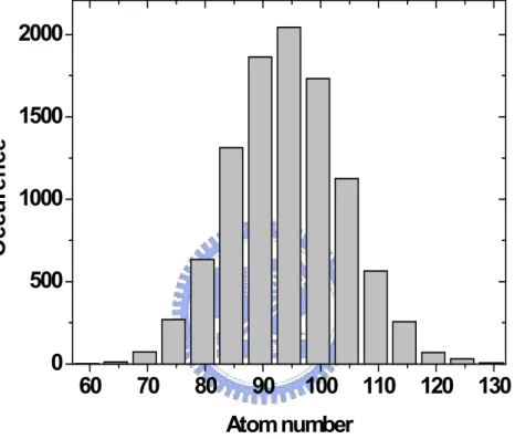
Dopant number fluctuation is governed by the Poisson function [8] shown in Fig. 2.1 and its functional form is as follows:
mean
mean
p( ,mean)
!
xe
x
x
−⋅
=
(2.1)mean dopant number N V dopant number
σ
= = × (2.2), where N is channel doping concentration and V is the volume of channel region.
To observe how dopant number fluctuation affects device performance, we should convert
σ
dopant numbertoσ
doping concentration by:dopant number doping concentration
N V
N
V
V
V
σ
σ
=
=
×
=
(2.3)From (2.3), it can be seen that the devices with heavily doped channel and small channel volume will suffer severe dopant number variation.
For position component, we may keep dopant number the same and randomly place dopants in the channel region. Fig. 2.2 and Fig. 2.3 are the demonstrations of dopant position distribution under two different doping concentrations. It can be seen that as dopant number becomes less (lightly doped devices), dopant position variation will become pronounced.
2.2 Methodologies
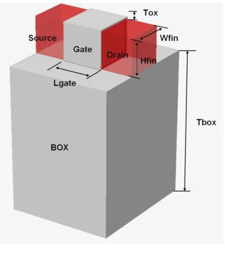
Our multi-gate MOSFETs are designed with Lg=25nm and total width
(2 H× fin+Wfin) equals to 75nm. Fig. 2.4 shows the perspective view and geometry definitions of a multi-gate SOI transistor. In our work, three aspect ratio (AR = Hfin /
Wfin) devices are investigated with the same total width:Quasi-planar (AR = 0.5),
Tri-gate (AR = 1) and FinFET (AR = 2). Besides, we also discuss device variability at two doping concentrations, 1 10 and 6 10 cm× 17 × 18 -3 . To sustain satisfactory electrostatic integrity, we use high-k gate dielectric with k = 25 and thigh-k = 2nm in
lightly doped devices.
Furthermore, to capture the statistical characteristic of device fluctuation, performing Monte Carlo simulation with sufficient ensembles is required to reflect the actual phenomena. Small number of samples may result in misleading conclusions but too many samples will lead to huge computation burden. In [15], E. Baravelli et. al. claimed 100 samples were adequate to achieve a clear trend, but in [18], A. Asenov collected 200 ones. In this work, we take 150 devices for every case.
For the convergence and efficiency concern, except for the conditions mentioned, we use drift-diffusion transport equation with constant mobility model throughout the work. Obviously, these physical models can not correctly capture the non-equilibrium carrier behavior and ballistic transport effects in such scaled devices. However, drift-diffusion is believed to be applicable in analyzing threshold voltage variations near sub-threshold region where the fluctuations are mainly determined by device electrostatic behaviors [19]. Besides, to compensate the error induced by the constant mobility approximation (without considering mobility degradation), we
extract threshold voltage at a higher current criterion, Ioff 300(W) nA L
= .
2.2.2 Atomistic Simulation Approaches
In this section, we will introduce three RDF simulation approaches and discuss their relationship in the following section.
Full Monte Carlo Simulation
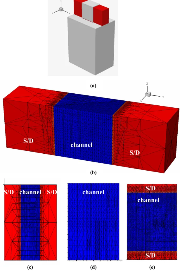
Our full Monte Carlo approach is similar to the one described in [20]. We build a large matrix equivalent to the lattice structure in the device channel region and assign a random number for each matrix element (lattice site). By comparing each random number with the probability defined as the ratio of original dopant number ( N V× ) to the number of total lattice site, the lattice matrix can be constructed as in Fig. 2.5.
After determining the placement of dopant atoms, we need to convert dopant atom to doping concentration by dividing by the corresponding small volume around each dopant, usually equals to the mesh size. Then we can translate this lattice dopant matrix to the channel doping matrix for 3-D device simulation [21]. Theoretically, we should construct uniform mesh to ensure the dopant arrangements are randomly distributed [18]. However, we can not generate perfect uniform mesh from TCAD simulation because the TCAD mesh generator tends to create finer meshes near the
the TCAD mesh command adjustments and the averaged volume defined as the ratio of the channel-region volume to the number of total meshes inside the region. In Fig. 2.6, we illustrate the quasi-uniform meshes generated from the refined TCAD device simulations.
Monte Carlo Simulation of Dopant Number Fluctuation
Based on the Poisson’s function in (2.1), we collect data from 150 devices each with different dopant number. Then we convert individual dopant number inside the device to doping concentration and perform the conventional continuous simulations. Fig. 2.7 shows the simulation flow described above.
Monte Carlo Simulation of Dopant Position Fluctuation
To extract pure position component, we keep dopant number fixed ( N V× ) for each device and randomly place dopants in the channel region as shown in Fig. 2.2 and Fig. 2.3. Then we convert the lattice dopant matrix to the channel doping matrix as described in the full Monte Carlo section for TCAD simulation use. Fig. 2.8 is the simulation flow of this method.
Verification
To validate our simulation results, we duplicate one of the conditions in [18], planar MOSFET with Weff = Leff = 50nm, NA = 5×1018 cm-3, and tox = 3nm. Fig. 2.9 is
the channel region. It can be seen that the potential in the SiO2/Si interface is
disturbed by the discrete dopants and this is the cause of threshold voltage variation. From Table 2.1, except for the inconsistency in the average threshold voltage, our threshold voltage fluctuation results are in a good agreement with what has been reported in [18].
2.3 Results and Discussions
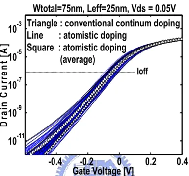
In Fig. 2.10, we perform 150 atomistic full Monte Carlo simulations and compare their average with the conventional continuous simulation. A threshold voltage lowering for the atomistic one can be seen (Table 2.2). Since in our simulations we did not consider the long-range Coulomb potential modification for each discrete dopant as described in [22], the threshold voltage lowering may come from the current percolation through the inhomogeneous potential induced by atomistic dopants [8] [18] and mobile carrier trapping due to the delta-like short-range atomistic Coulomb potential [22].
Fig. 2.11 shows the histogram plots of Vth variation before and after
Source/Drain swapping. Similar to [8] with only 24 samples and biased at VDD = 1.5V,
it makes no difference when interchanging Source/Drain in both lightly and heavily doped devices. However, if we observe the threshold voltage difference for every single device before and after swapping, it can be seen that the spread of threshold voltage difference for lightly doped devices (11.8 mV) is much larger than that of the heavily doped ones (2.54 mV) as shown in Fig. 2.12. This is because dopant
arrangements are different in view of source and drain especially for lightly doped devices. The phenomenon may need to be considered in circuit applications.
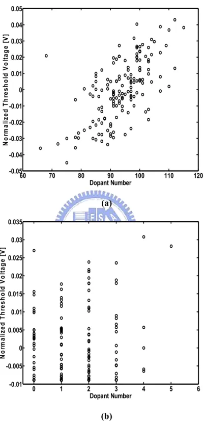
In Fig. 2.13, we show the correlation between the normalized threshold voltage, derived from the full Monte Carlo RDF simulation then normalized to their average, and the dopant number for heavily and lightly doped Tri-gate devices, respectively. The correlation coefficient for lightly doped devices (0.21) is much smaller than that of the heavily doped ones (0.64). This implies that the threshold voltage fluctuations can not merely be attributed to the dopant number variations. In Fig. 2.14, we demonstrate that the threshold voltage variation obtained from the full Monte Carlo (
σ
V
th,FMC) exactly consists of two components:number fluctuation(
σ
V
th,number) [23] and position fluctuation (σ
V
th,position) [24]. We confirm that the number and position components are mutually independent mechanisms. It also shows that our full Monte Carlo simulation can capture both the number and position fluctuations. Using full Monte Carlo simulation would be a more efficient way to accurately determine the overall RDF. Furthermore, through the full Monte Carlo simulation algorithm, we can easily formulate this procedure by the binomial equation :p k
( )
n
p
k(1
p
)
n kk
−
=
−
(2.4), where n is the number of lattice site and p is the probability defined as the ratio of the expected dopants to the total number of lattice sites.
When
n
→ ∞
,
np
→ < ∞
λ
, the binomial distribution converges to Poisson distribution [25], i.e.lim
(1
)
!
x x n x n npn
e
p
p
p
x
λ λλ
− − →∞ →
−
≈
(2.5)This explains the usage of Poisson distribution in the determination of random dopant number fluctuations.
To quantify the importance of the dopant position component, we define a ratio as [24]: th,position 2 position th,FMC
V
R
(
)
V
σ
σ
=
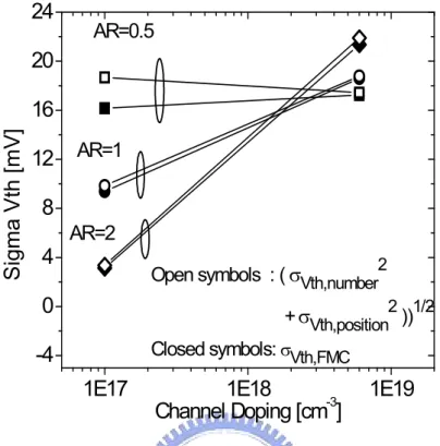
(2.6)It can be seen from Fig. 2.15 that
R
position is larger in lightly doped devices.Unlike the results in [24], our calculated
R
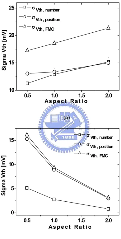
position can reach as high as 0.9 in lightly doped devices and about 0.5 in heavily doped devices. Even in the heavy doping case, the position component still accounts for nearly half of the total RDF. This means that merely treating the dopant number is not enough to accurately describe the overall RDF effects.Fig. 2.16 (a) shows that for heavily doped devices, threshold voltage variations increase with AR for both number and position components. This is because under the same doping concentration and total width, devices with AR = 0.5 have larger channel
volume than the AR =1 and AR = 2 ones. According to (2.3), the dopant number fluctuations would aggravate in devices with smaller volume [26]. For position component, smaller volume devices have less dopant inside the channel which would enhance the position RDF mismatch as shown in Fig. 2.2 and Fig. 2.3. In Fig. 2.16 (b), we demonstrate the AR dependence of threshold voltage variations for lightly doped devices. Threshold voltage fluctuations decrease as AR increases for both number and position components. This is because under nearly identical dopant number (about 1~2 dopants for different AR devices) and poor electrostatic integrity (due to lighter channel doping) conditions, the electrostatic integrity improvement with higher AR is the dominant mechanism for the reduction of both number and position RDF [27].
In Fig. 2.17, we investigate the dependence of threshold voltage fluctuations on channel doping. Instead of monotonically increasing with higher doping concentration [5], there is a worst case occurring at a moderate doping level. Generally speaking, higher channel doping can improve device electrostatic integrity but, at the same time, enhance RDF as well. Furthermore, better electrostatic integrity has been demonstrated to suppress the RDF [27]. It seems that for devices with better electrostatic integrity (such as AR = 2), increasing the channel doping results in less electrostatic integrity improvement but more RDF effects. For those poorer electrostatic integrity devices (such as AR = 0.5), increasing the doping may significantly improve electrostatic integrity and therefore reduce RDF. As we can see from the figure, poorer electrostatic integrity devices have a more pronounced peak.
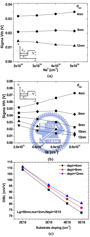
In [28], planar MOSFETs with epitaxial and delta-doped channels were suggested to reduce random dopant-induced threshold voltage variations. As shown in Fig. 2.18 (a) (b), the RDF can be suppressed at deeper epitaxial layer, depi. Besides,
for thinner epitaxial layers,
σ
Vth increases with doping concentration. However, devices with thicker epitaxial layers would behave anomalously: Vthσ
decreases with increasing doping concentration. A. Asenov et. al attributed this to the screening effect of the random dopant charge. However, we can also interpret the phenomenon using electrostatics. As shown in Fig. 2.16 (c), thinner epitaxial layer devices have better electrostatic integrity than thicker ones.
2.4 Modified Atomistic Simulation
In this section, we will introduce the concept of long-range and short-range Coulomb potential separation proposed by N. Sano et. al. [22] [29] which is a modification for the primary atomistic simulation. Then we will describe another revision of atomistic simulation proposed by [30].
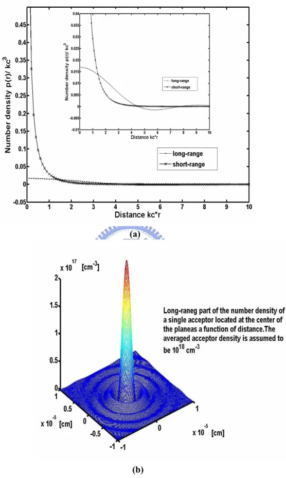
Due to the delta-like dopant charge induced by the discrete dopant, the subsequent sharp Coulomb potential would violate the drift-diffusion assumptions which should be the long-range Coulomb potential and the gradually changing band-gap. Besides, this singular short-range potential may result in the strong trapping of mobile carriers and screening of ionized dopants which lowers the effective channel doping. N. Sano. et. al. argued that this is the consequence of threshold voltage lowering shown in [8] [18]. It is suggested that using their long-range potential correction can resolve these problems. Finally, they demonstrated that their atomistic results are consistent with the continuous simulation counterparts for larger devices. Fig. 2.19 shows the plot of long-range and short-range doping concentration and the corresponding functional forms are as follows︰
3 long-range atomistic 2 3
sin(
)
(
)cos(
)
( )
2
(
)
c c c c ck
k r
k r
k r
r
k r
ρ
π
−
=
(2.7) 3 short-range atomistic( )
4
c k r c ck e
r
k r
ρ
π
−=
(2.8), where kc is the inverse of screen length and it determines the spread of long-range
component.
However, the choice of kc is somewhat ambiguous [29]. This brings
uncertainty for this method since different kc may lead to different results [31].
Actually, screen length should be derived from the full-band ensemble Monte Carlo coupled with the molecular dynamics (FB EMC/MD) simulation which deals with electron-impurity scattering events. Unfortunately, it is really time consuming and impractical for us to use.
Based on our simulations, smaller mesh size would give rise to severer carrier trapping and dopant screening. G. Roy et. al. [30] suggested that using density gradient model in the primary atomistic simulations can effectively remove either potential or carrier concentration mesh size dependence and singular dopant potential. After using this treatment, they still can find threshold voltage lowering and this is the evidence that threshold voltage lowering is not an artificial phenomenon. From their demonstration, the density gradient modification seems to be a simpler way to accurately simulate atomistic dopant problems. However, when coupling with atomistic simulation and density gradient approximation, the simulation convergency may significantly be degraded. So far, how to provide a more practical method for
both accuracy and efficiency is still an open question.
2.5 Summary
We have provided an assessment of random dopant fluctuations in multi-gate MOSFETs using atomistic simulations. Our full Monte Carlo approach can capture both number and position fluctuations. This is a more efficient and recommended method. Besides, threshold voltage lowering with respect to the continuous simulation is observed in our work. We believe it is due to current percolation in the inhomogeneous potential profile. Furthermore, Source/Drain asymmetry is another characteristic of atomistic simulation especially in lightly doped devices. This has rarely been discussed and may limit the application of switching circuit designs.
In lightly doped devices, position variation is the dominant mechanism and devices with larger AR will lead to less fluctuation due to better electrostatic integrity. In heavily doped devices, number and position components are comparable and the implementation of full Monte Carlo simulation is required. With higher AR, RDF becomes worse due to smaller channel volume and fewer dopants. Our study indicates that lightly doped FinFET, with its superior electrostatic integrity, is the best candidate for future multi-gate device design under the consideration of random dopant fluctuation.
Fig. 2.1 Poisson distribution of the dopant number inside the active region. The figure includes 10000 ensembles with 94 mean dopants.
60
70
80
90
100
110
120
130
0
500
1000
1500
2000
O
c
c
u
re
n
c
e
Atom number
0 50 100 150 200 250 300 350 400 0 5 10 15 20 25 30 35 40
Channel direction lattice
D e p th d ir e c ti o n l a tt ic e 0 50 100 150 200 250 300 350 400 0 5 10 15 20 25 30 35 40
Channel direction lattice
D e p th d ir e c ti o n l a tt ic e 0 50 100 150 200 250 300 350 400 0 5 10 15 20 25 30 35 40
Channel direction lattice
D e p th d ir e c ti o n l a tt ic e
Fig. 2.2 Top view of 3D random dopant arrangements with 120 dopants inside
the region. Closed circles represent dopant atoms. Demonstrated device dimensions are Lg = 100 nm, TSOI = 10nm and Wg = 40nm with doping =
18
0 50 100 150 200 250 300 350 400 0 5 10 15 20 25 30 35 40
Channel direction lattice
D e p th d ir e c ti o n l a tt ic e 50 100 150 200 250 300 350 400 0 5 10 15 20 25 30 35 40
Channel direction lattice
D e p th d ir e c ti o n l a tt ic e 0 50 100 150 200 250 300 350 0 5 10 15 20 25 30 35 40
Channel direction lattice
D e p th d ir e c ti o n l a tt ic e
Fig. 2.3 Top view of 3D random dopant arrangements with 4 dopant atoms inside the region. Closed circles represent dopant atoms. Demonstrated device dimensions are Lg = 100 nm, TSOI = 10nm and Wg = 40nm with
doping = 17
Fig. 2.4 Perspective view and geometry definitions of the multi-gate MOSFET used in this work.
Aspect Ratio (AR) = H /W fin fin
total fin fin
0
10
20
5
15
25
0
5
10
15
0
10
20
30
5
15
25
Channel length [nm]
Fin width [nm]
F
in
h
e
ig
h
t
[n
m
]
Fig. 2.5 Example of atomistic dopant placement in the channel region of a multi-gate MOSFET with Lg=25nm, Wfin=15nm, Hfin=30nm. Closed
Fig. 2.6 Our quasi-uniform meshes used for 3-D RDF device simulations in (a) (b) (c) (d) (e)
channel
S/D
S/D
channel
channel
channel
S/D
S/D
S/D
S/D
Dopant number
Poisson
distribution
#
dopant number1#
dopant number2#
dopant number3…
=
Dopant number
N
active region volume
N
2N
1N
3 0 5 10 15 0 5 10 15 20 25 0 5 10 15 20 25 30 0 5 10 15 0 5 10 15 20 25 0 5 10 15 20 25 30 0 5 10 15 0 5 10 15 20 25 0 5 10 15 20 25 30×
Fixed Dopant number
(N V)
….
Fig. 2.7 Simulation approach for dopant number fluctuation.
Fig. 2.9 Potential distribution at Si/SiO2 interface with discrete dopants inside
the channel. Potential distribution is distorted due to discrete dopants and this is the cause of threshold voltage variation.
-0.4
-0.2
0
0.2
0.4
10
-510
-310
-710
-910
-11Gate Voltage [V]
D
ra
in
C
u
rr
e
n
t
[A
]
Wtotal=75nm, Leff=25nm, Vds = 0.05V
Triangle : conventional continum doping
Line : atomistic doping
Square : atomistic doping
(average)
Ioff
Fig. 2.10 Id-Vg curves for conventional simulation (Triangle), 150 atomistic simulations (solid lines) and the average of these atomistic simulations
(square).
Table2.2. Detailed data of Vth shift and Vth variations for devices
with Lg = 25 nm and Wtotal = 75nm. Vth lowering is defined
0 5 1 0 1 5 2 0 2 5 0 . 5 9 F re q u e n c y T h r e s h o l d V o l t a g e [ V ] F o r w a r d S / D R e v e r s e S / D 0 . 6 1 0 . 6 3 0 . 5 7 0 . 5 5 0 1 0 2 0 3 0 4 0 5 0 F re q u e n c y T h r e s h o l d V o l t a g e [ V ] F o r w a r d S / D R e v e r s e S / D 0 . 2 5 0 . 2 6 0 . 2 4 0 . 2 3 (a) (b)
Fig. 2.11 Histogram plots of S/D swapping with 150 microscopically different (a) heavily doped and (b) lightly doped Tri-gate devices. Here forward means before S/D swapping operation and reverse means after S/D
-10 -5
0
5
10 15 20 25 30
0
10
20
30
40
50
60
70
80
F
re
q
u
e
n
c
y
S/D Vth difference [mV]
S/D σσσσ Vth diff.= 2.54 mV-50 -40 -30 -20 -10 0
10 20 30 40
0
10
20
30
40
S/D
σσσσ Vthdiff. = 11.80 mV
F
req
u
e
n
cy
S/D Vth difference [mV]
(a) (b)Fig. 2.12 Histogram plots of Vth difference between S/D swapping for (a) heavily doped and (b) lightly doped Tri-gate MOSFETs
(b) (a)
Fig. 2.13 The correlation coefficients between the normalized threshold voltages and the dopant number are (a) 0.64 for heavily doped and (b) 0.21 for lightly doped Tri-gate devices.
60 70 80 90 100 110 120 -0.05 -0.04 -0.03 -0.02 -0.01 0 0.01 0.02 0.03 0.04 0.05 Dopant Number N o rm a li z e d T h re s h o ld V o lt a g e [ V ] 0 1 2 3 4 5 6 -0.01 -0.005 0 0.005 0.01 0.015 0.02 0.025 0.03 0.035 Dopant Number N o rm a li z e d T h re s h o ld V o lt a g e [ V ]
1E17
1E18
1E19
-4
0
4
8
12
16
20
24
S
ig
m
a
V
th
[
m
V
]
Channel Doping [cm
-3]
AR=0.5 AR=1 AR=2Open symbols : ( σVth,number2
+ σVth,position2 ))1/2 Closed symbols: σ Vth,FMC
0.5
1.0
1.5
2.0
0.5
0.6
0.7
0.8
0.9
1.0
R
p o s it io nAspect Ratio
Lightly doped
Heavily doped
Lgate=25nm
Wtotal = 75nm
Vds = 0.05V
Fig. 2.14 Our full Monte Carlo simulation can capture both number and position fluctuations.
Fig. 2.15 Dependence of Rposition on different AR multi-gate devices
0.5 1.0 1.5 2.0 10 15 20 25 σσσσ Vth , number σ σσ σ Vth , position σ σσ σ Vth , FMC S ig m a V th [ m V ] A s p e c t R a t i o 0.5 1.0 1.5 2.0 0 5 10 15 Si g m a Vt h [ m V] A s p e c t R a t i o σ σ σ σ Vth , number σ σ σ σ Vth , position σ σ σ σ Vth , FMC (b) (a)
Fig. 2.16 The AR dependence of threshold voltage fluctuations for (a) heavily doped and (b) lightly doped devices.
1E16 1E17 1E18 1E19 0 10 20 30 40 50 S ig m a V th [ m V ] Doping concentration [cm-3] AR=0.5 AR=1 AR=2 L=25nm,Wtotal=75nm tgate(SiO2)=1nm,Vds=0.05V th th
V
V
N
N
d
d
d
σ
=
⋅
n
n
N V
N
N
V
V
V
V
d
=
∆
=
=
⋅
=
n : dopant number
N : doping concentration
Fig. 2.17 Doping dependence of threshold voltage variation for 3 AR devices. Threshold voltage variations are determined by the electrostatic integrity and doping concentration.
2.0x10¹² 4.0x10¹² 6.0x10¹² 8.0x10¹² 0.00 0.01 0.02 0.03 0.04 0.05 0.06 0.07 0.08 0.09 12nm 10nm 8nm 6nm 4nm depi S ig ma V th [ V ] Qδδδδ [cm-2]
Fig. 2.18 Threshold voltage variation as a function of the (a) doping concentration NA b
behind the epi-layer and (b) delta-doping dose Qδ for a set of 50×50nm
MOSFET’s with t = 3nm,NA b
= 1×1018 cm-3, NA e
= 1×1015 cm-3, at different epi-layer thickness [28]. Inset plot shows the definition of epi-layer. (c) shows
(a) (b) (c) 2x10¹⁸ 3x10¹⁸ 4x10¹⁸ 5x10¹⁸ 0.00 0.01 0.02 0.03 0.04 S ig m a V th [ V ] Nab [cm-3] d epi 4nm 8nm 12nm
2E18 3E18 4E18 5E18 70 75 80 85 90 95 100 105 110 115 D IB L [ m V /V ] Substrate doping [cm-3] depi=4nm depi=8nm depi=12nm Lg=50nm,tox=3nm,Nepi=1E15
(a)
(b)
Fig. 2.19 (a) 1D representation of long-range and short-range parts of the dopant number density and (b) 3D perspective view of long-range part number density. Long-range potential does not diverge at the origin.
Chapter 3
Line Edge Roughness
and
Equivalent Oxide Thickness Variation
3.1 Line Edge Roughness
3.1.1 Introduction
Due to the resolution limit of lithography, etching process or the grain characteristic of photo resist and poly gate, it’s inevitable to generate line edge roughness (LER) during device processing. This effect was negligible in the past. However, it is becoming increasingly important for scaled devices. According to the ITRS predictions in 2007 [2], the tolerance of LER for 65nm and 32nm node is 2.6nm (3σ) and 1.3nm, respectively. Unfortunately, the best technology in the world can only provide about 5nm LER in 2003 [10]. LER will soon become comparable to device critical dimension and may worsen device short channel effects. Actually, under the prediction of recent studies [30], LER is expected to become the dominant contributor to device variation for future planar MOSFETs.
In the past, several approaches were adopted to estimate the effects of LER. For example, P. Oldiges et al. [32] employed simplified 2D slice simulations to capture the behaviors of real ragged 3D devices. C. H. Diaz et al. [33] derived an
the model with experimental data. A. Asenov et al. [10], for the first time, provided a systematic 3D discussion of LER and investigated the relative contribution of RDF and LER to the overall intrinsic parameter fluctuations for planar MOSFETs. However, a detailed and comprehensive exploration of LER for multi-gate transistors is still needed. Although E. Baravalli et. al. [34] [15] gave a sophisticated simulation on FinFET and concluded that fin- and gate- LER would become significant as compared to RDF below 45-nm gate length geometries, it is still unclear how LER will influence these highly geometry-dependent devices with different AR design or doping concentration. This is one of the main purposes in this work.
In the following sections, we will first introduce the methodology for the LER simulation. For a given gate length and total width, we examine the impacts of simulation parameters on the threshold voltage for heavily and lightly doped devices. Finally, we provide a comparison of LER with RDF for different doping and device structures.
3.1.2 Methodologies
3.1.2.1 Concept
The causes of LER, such as lithography, etching and diffusion, are similar to low-pass filters during transferring the rough line pattern to devices. Due to the isotropic properties, they could smooth the original rough pattern of photo resist or mask, as revealed from the magnitude of real line edge pattern in frequency domain shown in Fig. 3.1. Based on this characteristic, we can model the behavior of the
magnitude spectrum associated with appropriate phases to reconstruct the LER patterns. This is the concept of Fourier synthesis approach [9-10].
3.1.2.2 Simulation Approach
The most popular model to simulate the magnitude spectrum of LER is the Gaussian and exponential autocorrelation functions with two parameters:
S
G( )
k
=
π
∆ Λ
2e
−(k2Λ2/ 4) (3.1) 2 2 22
( )
1
ES
k
k
∆ Λ
=
+
Λ
(3.2), where ∆ is the rms amplitude of the roughness, and Λ is the correlation length which is a fitting parameter for a particular type of LER. k is the index of discrete sampling points defined as k=i(2 / Ndx)π with dx the spacing of sampling points.
Fig. 3.2 shows a real LER power spectrum compared with the Gaussian and exponential models with the specified values of ∆ and Λ [10]. With appropriate choices of rms amplitude and correlation length combined with randomly selected phases that can make sure each rough line is unique, we can rebuild rough lines as shown in Fig. 3.3. It can be seen that the Gaussian model is smoother than the exponential one due to lack of high frequency component. Besides, unlike planar MOSFETs, multi-gate LER comes from both gate length and fin width dimension deviations. It has been confirmed that
σ
total_LER2 =σ
fin_LER2 +σ
gate_LER2 [34]. Fig.As for the determination of model parameters, the value of rms amplitude can be obtained from the ITRS. Unlike rms amplitude, the choice of correlation length should be extracted from the real line edge patterns. P. Oldiges et al. [32] reported that the values of correlation length vary between 10 and 50nm from their measurements. Based on the SEM analysis, A. Asenov et al. [10] indicated that the values of correlation length are in the range of 20-30nm. Due to lack of the experimental data, we determine the value of correlation length from the literatures mentioned above in the following simulations.
As in chapter 2, we perform Monte Carlo simulation with 150 samples to capture the stochastic behavior regarding LER. Besides, we use the same physical TCAD simulation models and current extraction criterion as in chapter 2. To relieve the simulation burden, we use continuous doping in the following simulations.
3.1.3 Results and Discussions
Before investigating the impacts of model parameters on device characteristics, we first qualitatively evaluate their influences on the LER patterns and try to gain more insights about the model. In Fig. 3.5, we set correlation length to 20nm with various rms amplitude values. It can be seen that increasing rms amplitude gives rise to larger amplitude spectrum. Moreover, from Fig. 3.5 (a) (b), we find the difference in amplitude spectrum is about four times when the rms amplitude becomes two times larger. This can be explained by (3.1). Besides, increasing the rms amplitude would
lead to rougher line as shown in Fig. 3.5 (c). In Fig. 3.6 (a), we vary the correlation length with constant rms amplitude. We can find that the magnitude spectrum with smaller correlation length would spread out to higher frequency region, which results in the rougher LER (more high frequency components) as observed in Fig. 3.6 (b). Moreover, in Fig. 3.6 (b), we find that increasing correlation length would also lead to worse LER (
σ
LER =1.23, 1.87 nmfor correlation lengths equal to 20 and 50nm).Fig. 3.7 shows the rms amplitude dependence of
σ
Vthfor lightly doped devices with 3 kinds of AR. It can be seen that increasing the rms amplitude, or rougher line edge, may result in severer threshold voltage variation for both gate and fin components. Besides, for devices with AR=0.5 or 1, gate LER is the dominant mechanism due to poor electrostatic integrity. With the increasing of AR, we can find that the influences of gate- and fin- LER become comparable in our FinFET (AR=2) devices. For devices designed with AR=5 as described in [34], fin LER would dominate the overall LER variation. In Fig. 3.8, we design the total width of FinFET (AR=2) devices to three times of Lg at different technology nodes and compare theimportance of gate and fin LER. It can be seen that the fin LER is the main contributor to device LER variations because of the significant shrinkage of fin width at smaller devices. From above discussions, we conclude that gate and fin LER will become dominant for devices with critical dimension in channel length and fin width, respectively.
In Fig. 3.9, we investigate the impacts of correlation length on device variation. Similar to the results in Fig. 3.7, increasing correlation length leads to higher Vth
variations induced by the fin LER will saturate as correlation lengths reach the gate length, 25nm, and gate LER shows different saturation levels because of the different fin widths for three various AR devices. This property is also observed in planar transistors [10]. To explain the phenomenon, we demonstrate three LER patterns associated with different correlation lengths as shown in Fig. 3.10. If we assume that the device critical dimension is equal to 50nm, and assign the corresponding LER pattern for each device as shown in the figure, it can be seen that as the correlation length decreases, the discrepancy of LER pattern for each device increases. This explains the initial increase for small correlation lengths. When the correlation length approaches the device critical dimension, there is less LER pattern dispersion and therefore the Vth variation saturates.
For heavily doped transistors, all of above characteristics are similar to lightly doped ones. In Fig. 3.11, we compare total LER (
σ
fin_LER2 +σ
gate_LER2 ) for deviceswith different doping concentration and AR. It can be seen that heavily doped devices show better immunity to LER because of the superior gate control especially for the devices with small AR. Moreover, increasing doping concentration can significantly suppress LER at the price of worse RDF as mentioned in chapter 2. Fig. 3.12 illustrates the comparison of RDF and LER. It can be seen that RDF dominates in heavily doped devices. For lightly doped devices, LER is the most important contributor to device variations. Under the consideration of RDF and LER, lightly doped FinFET (AR=2) has better immunity to device intrinsic parameter fluctuations.
So far, we have discussed several properties of LER and its influences on multi-gate devices. We tackle the problem with individual assessment of RDF and
LER, that is, we assume that they are independent events. Actually, this is confirmed in planar MOSFETs [10]. However, there are several studies against this argument. It is believed that there exist coupling between RDF and LER. S. Xiong et. al. [35] performed process simulation and found LER enhanced lateral diffusion. M. Hane et.
al. [36] considered both RDF and LER simultaneously and confirmed the existence of
coupling. To assess this problem, we make a simple examination of dopant number in the channel with different degree of LER. The determination of dopant number is similar to the full Monte Carlo simulation in section 2.2.2. Fig. 3.13 show the dopant number histogram plots with no LER, LER with rms amplitude=1.5nm and 2.5nm, respectively. It can be seen that different rough patterns have the same average but different spreading in dopant number. Rougher line edge pattern seems to be more diverse. This is because worse LER causes larger discrepancy in the channel volume which is closely related to the total dopant number. In other words, we may observe the coupling between RDF and LER in aspect of dopant number. We will further investigate the coupling between RDF and LER in the future.
3.2 Equivalent Oxide Thickness Variation
3.2.1 Introduction
To sustain gate control, reducing equivalent oxide thickness (EOT) is an effective way in scaled MOSFETs. When gate oxide is scaled to several atom layers, not only random dopant fluctuation and line edge roughness, surface roughness at the SiO2/Si and SiO2/gate interfaces will lead to significant local oxide thickness variation
and become another source of device variation. A. Asenov et. al. [11] implied that for conventional MOSFETs with dimensions below 30nm, threshold voltage fluctuations induced by oxide thickness variation are comparable to random dopant fluctuation. Later on, A. T. Putra et. al. [37] performed 3D simulations on atomic oxide roughness and local gate depletion and then concluded that oxide thickness variation is not the main origin of Vth variation in FDSOI MOSFETs.
Under the concern of gate leakage, using higher dielectric constant (high-k) materials in placement of conventional SiO2 insulator provides us an alternative for
device design [2]. Due to higher dielectric constant, we can retain the same gate coupling with thicker physical thickness and less local oxide thickness variation. However, the introduction of high-k gate stack may also bring several technological issues [38]. Some of these effects will introduce intrinsic parameter fluctuations such as the non-uniformity of dielectric constant over the gate stack [39].
In the following section, we will introduce our methodology in the investigation of the impacts of oxide thickness variation and high-k non-uniformity on multi-gate transistors. Finally, we will compare this mechanism with RDF and LER.
3.2.2 Methodologies
Oxide Thickness Variation (OTV)
OTV is simulated with the Fourier synthesis approach as described in LER section except for the modification of 1D line pattern to 2D roughness interface