國 立 交 通 大 學
電子工程學系電子研究所
博 士 論 文
適用於高低壓共容輸入輸出介面之積體電路
靜電放電防護設計
ESD PROTECTION DESIGNS FOR
MIXED-VOLTAGE I/O INTERFACES
IN CMOS INTEGRATED CIRCUITS
研 究 生 :林 昆 賢 (Kun-Hsien Lin)
指導教授 :柯 明 道 (Ming-Dou Ker)
適用於高低壓共容輸入輸出介面之積體電路
靜電放電防護設計
ESD PROTECTION DESIGNS FOR
MIXED-VOLTAGE I/O INTERFACES
IN CMOS INTEGRATED CIRCUITS
研 究 生:林昆賢
Student: Kun-Hsien Lin
指導教授:柯明道
Advisor: Ming-Dou Ker
國 立 交 通 大 學
電子工程學系電子研究所
博 士 論 文
A Dissertation
Submitted to
Institute of Electronics
College of Electrical Engineering
And Computer Science
National Chiao Tung University
For the Degree of Doctor of Philosophy
in
Electronic Engineering
January 2005
Hsinchu, Taiwan, Republic of China
適用於高低壓共容輸入輸出介面之積體電路
靜電放電防護設計
研究生:林昆賢 指導教授:柯明道
國立交通大學電子工程學系電子研究所
摘要
適用於高低壓共容輸入輸出介面(Mixed-Voltage I/O Interfaces)或具有
省電模式(Power-Down-Mode)功能之互補式金氧半積體電路(CMOS ICs)將
使得靜電放電
(Electrostatic Discharge, ESD)防護設計有更多的限制與困
難。適用於高低壓共容輸入輸出介面之積體電路,靜電放電防護設計必需
考慮在電路正常操作下,閘極氧化層(Gate Oxide)的可靠度問題與避免額外
的漏電流路徑;而具有省電模式功能之積體電路,靜電放電防護設計必需
考慮在省電模式操作下,避免額外的漏電流路徑與內部電路誤動作的發
生。在靜電放電發生時,靜電放電防護電路必需能夠有效地保護內部電路
防止內部電路受到損傷。此外,在高壓互補式金氧半製程技術中,靜電放
電防護元件的低持有電壓(Holding Voltage)特性將使得高壓積體電路發生
閉鎖效應(Latchup)或類似閉鎖效應(Latchup-Like)的危險。此問題將使得高
壓積體電路之靜電放電防護設計更加困難。另一方面,在奈米互補式金氧
半製程技術中,如何設計具較快導通速度且較小佈局面積的電源間靜電放
電箝制電路(Power-Rail ESD Clamp Circuit)來保護超薄的閘極氧化層以應用
在系統單晶片
(SOC)將是個挑戰。本論文將針對高低壓共容輸入輸出介
面、具有省電模式功能、高壓互補式金氧半製程技術、與奈米互補式金氧
半製程技術之積體電路靜電放電防護設計上的限制與困難作討論,並進一
步設計出有效的靜電放電防護電路在各相關應用之積體電路晶片。
為了提供有效的靜電放電防護於高低壓共容輸入輸出電路,本論文提
出利用基體觸發(Substrate Triggered)技術來提昇堆疊電晶體(Stacked-NMOS)
的靜電放電防護能力。利用基體觸發技術可使得堆疊電晶體的觸發電壓
(Trigger Voltage)降低,如此更能有效地保護高低壓共容輸入輸出電路。這
種利用基體觸發技術所設計靜電放電防護電路其製程步驟完全相容於一般
互 補 式 金 氧 半 導 體 的 製 程 , 且 不 需 要 使 用 厚 的 閘 極 氧 化 層 。 適 用 於
2.5V/3.3V 共容高低壓輸入輸出電路的靜電放電防護電路已在 0.25 微米互
補式金氧半製程中實際被製作與驗證。實驗結果顯示利用基體觸發技術所
設計靜電放電防護電路可使得堆疊電晶體的觸發電壓從
8.5 V 降低到 5.3
V;而高低壓共容輸入輸出電路在 240 微米總寬度的堆疊電晶體條件下,
其人體放電模式(Human-Body-Model, HBM)的靜電放電耐受能力可以從原
來的
3.4 kV 提昇到 5.6 kV。
為了提供有效的靜電放電防護於具有省電模式功能之積體電路晶片,
本論文提出新型的靜電放電防護電路架構。此靜電放電防護電路架構包括
一靜電放電匯流排(ESD Bus)與數個二極體(Diode),使得積體電路進入省
電模式操作下,可避免從輸入輸出焊墊(I/O Pad)到 VDD 電源線間的漏電流
路徑及內部電路誤動作的發生。當積體電路在正常操作下,此設計具有極
低的漏電流且不會影響到內部電路的正常工作。在此靜電放電防護電路架
構中,VDD 到 VSS 電源間以及靜電放電匯流排到 VSS 電源間,各有一組
靜電放電箝制電路以達到全晶片靜電放電防護設計的目的。在
0.35 微米互
補式金氧半製程中,此設計可達到
7.5 kV 的人體放電模式靜電放電耐受能
力。此外,在此靜電放電防護電路架構中,本論文也提出了改善輸出端電
壓準位的電路,使得內部電路在正常操作下輸出端的最高電壓可以達到
VDD 的電壓準位。
在高壓互補式金氧半製程技術中,金氧半場效電晶體(MOSFET)、矽
控整流器(SCR)或者是雙載子電晶體(BJT),被廣泛的用作靜電放電防護元
件。但是這些靜電放電防護元件在驟回崩潰(Snapback Breakdown)狀態下
的持有電壓都遠小於高壓
Vcc 電源的電壓。此低持有電壓的元件特性將使
險,尤其是將這些元件用作電源間靜電放電箝制元件。本論文針對此問題
作深入的研究,並進一步提出新型的電源間靜電放電箝制電路以避免高壓
積體電路發生閉鎖效應或類似閉鎖效應的危險。此設計是藉由調整堆疊元
件的數目,使得堆疊元件結構在驟迴崩潰狀態下的箝制電壓超過高壓
Vcc
電源的電壓。如此,在不需要增加或改變製程步驟下,便可以達到避免高
壓積體電路發生閉鎖效應或類似閉鎖效應的目的。利用此概念設計的堆疊
場氧化層電晶體結構(Stacked Field-Oxide Structure)用在電源間靜電放電箝
制電路已經在供應電壓為
40 V 的 0.25 微米互補式金氧半製程中驗證,其能
有效地防止高壓積體電路發生閉鎖效應或類似閉鎖效應的危險。
為了在奈米金氧半製程技術中實現具較高靜電放電耐受能力且較小佈
局面積的輸入輸出單元(I/O Cell),本論文在 0.13 微米互補式金氧半製程
中,提出使用電源間寄生矽控整流器來作為電源間靜電放電箝制元件的輸
入輸出單元。本論文共提出兩種寄生矽控整流器結構,其在電路正常操作
下並沒有閉鎖效應的問題。在佈局上,此寄生矽控整流器結構是放置於輸
入輸出單元的輸入(或輸出)P 型電晶體與 N 型電晶體之間。此外,寄生矽
控整流器的導通速度可經由基體觸發技術而明顯的提昇。在
0.13 微米互補
式金氧半製程中,此設計可達到
5 kV 的人體放電模式靜電放電耐受能力。
此設計讓每個輸入輸出單元都具有一個快導通速度且高靜電放電耐受能力
的電源間靜電放電箝制元件,因此在單一的輸入輸出單元便可以提供全晶
片靜電放電防護所需之放電路徑。利用此設計,晶片可在較小的佈局面積
下具有更高的靜電放電耐受能力。
在本博士論文中,已經針對高低壓共容輸入輸出介面、具有省電模式
功能、高壓互補式金氧半製程技術、與奈米互補式金氧半製程技術等應用
之積體電路設計出高效能的靜電放電防護電路。所設計的靜電放電防護電
路均已在實際晶片上成功驗證,並有相對應的國際期刊論文發表與專利申
請。
ESD PROTECTION DESIGNS FOR
MIXED-VOLTAGE I/O INTERFACES
IN CMOS INTEGRATED CIRCUITS
Student: Kun-Hsien Lin Advisor: Ming-Dou Ker
Department of Electronics Engineering and Institute of Electronics
National Chiao Tung University
ABSTRACT
For the CMOS integrated circuits (ICs) with the mixed-voltage I/O interfaces or power-down-mode application, the on-chip electrostatic discharge (ESD) protection circuits will meet more design constraints and difficulties. The on-chip ESD protection circuit for mixed-voltage I/O interfaces should meet the gate-oxide reliability constraints and prevent the undesired leakage current paths during normal circuit operating operation, whereas that for IC with power-down-mode operation should avoid the undesired leakage current paths and malfunction during power-down-mode operation. During ESD stress condition, the on-chip ESD protection circuit should provide effective ESD protection for the internal circuits. In high-voltage CMOS technology, the low-holding-voltage characteristic of ESD protection devices has been found to cause the high-voltage CMOS ICs susceptible to latchup or latchup-like danger during normal circuit operating condition. How to avoid the latchup or latchup-like failure in high-voltage CMOS ICs will be an important challenge to on-chip ESD protection design for high-voltage CMOS IC products. In nanoscale CMOS technology, how to realize the turn-on-efficient and area-efficient power-rail ESD clamp circuit to protect the ultra-thin gate oxide will be an important challenge to system-on-a-chip (SOC) applications with a much larger chip size. In this thesis, the ESD design constraints in mixed-voltage I/O interfaces, power-down-mode application, high-voltage CMOS technology, and nanoscale
CMOS technology are presented. Furthermore, the novel on-chip ESD protection circuits have been developed to overcome the design constraints in such applications.
To provide effective ESD protection in the mixed-voltage I/O interfaces, a new ESD protection design, by using the substrate-triggered stacked-nMOS device, is proposed to protect the mixed-voltage I/O circuits of CMOS ICs. The substrate-triggered technique is applied to reduce the trigger voltage of the stacked-nMOS device for ensuring effective ESD protection for the mixed-voltage I/O circuits. The proposed ESD protection circuit with the substrate-triggered technique is fully compatible to general CMOS process without causing the gate-oxide reliability problem. Without using the thick gate oxide, the new proposed design has been fabricated and verified for 2.5V/3.3V-tolerant mixed-voltage I/O circuit in a 0.25-µm salicided CMOS process. By using this substrate-triggered design, the trigger voltage of the stacked-nMOS device can be reduced from the original 8.5V to become 5.3V to ensure effective protection for the mixed-voltage I/O circuits. The human-body-model (HBM) ESD level of the mixed-voltage I/O buffer with a stacked-nMOS of 240-µm channel width can be improved from the original 3.4 kV up to 5.6 kV by this substrate-triggered circuit.
To provide effective ESD protection for power-down-mode application, a new design on the ESD protection schemes for CMOS IC operating in power-down-mode condition is proposed. By using an additional ESD bus and diodes, the new proposed ESD protection schemes can block the leakage current from I/O pad to VDD power line to avoid malfunction during power-down-mode operating condition. During normal circuit operating condition, the new proposed ESD protection schemes have no leakage path to interfere with the normal circuit functions. The whole-chip ESD protection design can be achieved by insertion of ESD clamp circuits between VSS power line and both VDD power line and VDD ESD bus line. Experimental results have verified that the HBM ESD level of the new schemes can be greater than 7.5kV in a 0.35-µm silicided CMOS process. Furthermore, the output signal of the proposed ESD protection schemes can be successfully pulled up to VDD again by the output-swing improvement circuit under normal circuit operating condition.
In high-voltage CMOS technology, high-voltage MOSFET, silicon controlled rectifier (SCR) device, and bipolar junction transistors have been widely used as on-chip ESD protection devices. The double snapback characteristic in the high-voltage nMOSFETs has been investigated and analyzed by both measured and simulation results. Furthermore, the holding voltage of the high-voltage devices in snapback breakdown condition has been found to be much smaller than the high-voltage power supply voltage. Such characteristics will
cause the high-voltage CMOS ICs susceptible to the latchup or latchup-like danger in the practical system applications, especially while these devices are used in the power-rail ESD clamp circuits between the high-voltage power lines. In this thesis, the latchup or latchup-like issues in high-voltage CMOS ICs have been investigated in details. By adjusting different numbers or different types of stacked ESD devices in the power-rail ESD clamp circuits, the total holding voltage of the stacked structure can be designed higher than the high-voltage supply voltage without using extra process modification in the high-voltage CMOS technology. A new latchup-free design on the high-voltage power-rail ESD clamp circuit with stacked field-oxide structure is proposed and successfully verified in a 0.25-µm 40-V CMOS process to achieve the desired ESD level. Therefore, latchup or latchup-like issues can be avoided by stacked field-oxide structures for the IC applications with power supply of 40V.
In order to realize the high-ESD-robust and high-area-efficient I/O cells in nanoscale CMOS technology, a new ESD protection design for I/O cells with embedded SCR structure as power-rail ESD clamp device in a 130-nm CMOS process is proposed. Two new embedded SCR structures without latchup danger are proposed to be placed between the input (or output) pMOS and nMOS devices of the I/O cells. Furthermore, the turn-on efficiency of embedded SCR can be significantly increased by substrate-triggered technique. Experimental results have verified that the HBM ESD level of this new proposed I/O cells can be greater than 5kV in a 130-nm fully salicided CMOS process. By including the efficient power-rail ESD clamp device into each I/O cell, whole-chip ESD protection scheme can be successfully achieved within a small silicon area of I/O cell. Such I/O cells are very suitable for SOC applications in nanoscale CMOS technology.
In summary, the novel ESD protection designs have been successfully developed for mixed-voltage I/O interfaces, power-down-mode application, high-voltage CMOS technology, and nanoscale CMOS technology with high ESD robustness. Each of the proposed ESD protection circuits has been practically verified in the silicon testchips.
誌 謝
首先要感謝我的指導教授柯明道教授三年多來的耐心指導與鼓勵,使
我能夠順利完成博士學業。在指導教授循序漸進的教誨下,讓我得以在積
體電路靜電放電防護設計的領域中,由入門到能夠獨立解決問題。此外,
指導教授認真的研究態度與嚴謹的處事原則,也讓我學習到挑戰困難解決
問題的正確態度與方法。雖然在過程中倍感艱辛,也經歷了不少挫折,然
而卻讓我獲益良多,更促使我成長。此外還要感謝實驗室的吳重雨教授給
我的許多指導與建議。
在這段求學的過程中,『工研院系統晶片技術發展中心』的『產品與
靜電防護技術部』給予我的研究最大的支持與協助,從實驗晶片的下線及
量測設備的支援協助,都是使得我實驗研究能夠順利完成的主要原因。在
此特別感謝吳文慶組長、江志強經理、翁季萍經理、彭政傑課長、莊哲豪
課長所給予的支持與鼓勵,也要感謝陳子平、曾當貴、陳世宏、黃柏獅、
林明芳、劉美竹、鍾瑞玲、劉玉珠以及曾任職於工研院的姜信欽博士、張
智毅、蔡燿城、侯春麟在實驗上的協助,使我的研究論文能夠在國際上順
利發表,獲得肯定。
此外,也要感謝『奈米電子與晶片系統實驗室』的陳東暘博士、徐國
鈞博士、莊健暉、羅文裕、陳世倫、鄧至剛、徐新智、許勝福、張瑋仁、
陳榮昇、陳穩義、吳偉琳諸位實驗室學長、同學及學弟妹們,在我博士班
的這一個階段,於各方面給了我不少的幫忙,使得我能順利完成我的論文
以及在知識及處事上有所成長。也感謝實驗室助理卓慧貞小姐在實驗室行
政事務上的許多協助。
最後,我要致上我最深最深的感謝給予我的父親林昌德先生、母親賴
貴英女士、岳父戴文謁先生、岳母戴張足女士、哥哥林鼎晏先生、弟弟林
昀生先生、愛妻戴淑梅小姐,沒有你們無怨悔、永無止境的付出、鼓勵、
支持與照顧,就沒有我今日的成就,在此衷心地感謝你們。另外,要祝福
所有在這幾年與我相處過的師長、朋友、學弟妹們,有緣與你們同在這一
個階段成長,是我一生的榮幸,願大家都能順心如意,心想事成!
林 昆 賢
謹誌於竹塹交大
九十四年 一月
CONTENTS
ABSTRACT (CHINESE)
iABSTRACT (ENGLISH)
ivACKNOWLEDGEMENTS
viiCONTENTS
viiiTABLE CAPTIONS
xiFIGURE CAPTIONS
xiiCHAPTER 1 INTRODUCTION
11.1 Background 1
1.1.1 Issue of Mixed-Voltage I/O Interface 1
1.1.2 Issue of Power-Down Application 4
1.1.3 Issue of High-Voltage CMOS ICs 5
1.1.4 Issue of Nanoscale CMOS Technology 6
1.2 ESD Protection Designs for Mixed-Voltage I/O Interfaces 7
1.2.1 Substrate-Triggered Stacked-NMOS Device 7
1.2.2 Extra ESD Device between I/O pad and VSS 7
1.2.3 Extra ESD Device between I/O pad and VDD 9
1.2.4 ESD Protection Design with ESD Bus 10
1.2.5 Special Applications 11
1.3 Thesis Organization 12
Figures 15
CHAPTER 2 ESD PROTECTION DESIGN FOR MIXED-VOLTAGE
I/O CIRCUITS
262.1 Stacked-NMOS Device 26
2.2 Stacked-NMOS with Substrate-Triggered Technique 28
2.2.1 Substrate-Triggered Stacked-NMOS Device 28
2.2.2 ESD Protection Circuit 28
2.2.3 Operating Principles 29
2.3.1 Characteristics of the Substrate-Triggered Stacked-NMOS Device 31 2.3.2 Leakage Current 32 2.3.3 ESD level 33 2.4 Summary 33 Tables 35 Figures 36
CHAPTER 3 ESD PROTECTION DESIGN FOR IC WITH
POWER-DOWN-MODE OPERATION
453.1 New ESD Protection Schemes for IC with Power-Down-Mode Operation 45 3.1.1 ESD Protection Scheme I 45
3.1.2 ESD Protection Scheme II 47
3.1.3 ESD Protection Scheme III 48
3.1.4 Layout Consideration 48
3.2 Experimental Results 49
3.2.1 Leakage Current 49
3.2.2 Function Verification 50
3.2.3 ESD Robustness 51
3.3 Output-Swing Improvement Circuit 52
3.4 Summary 53
Tables 54
Figures 55
CHAPTER 4 ESD PROTECTION DESIGN IN HIGH-VOLATGE
CMOS PROCESS
674.1 Double Snapback Characteristics in High-Voltage NMOSFETs 67
4.1.1 Double-Snapback Characteristics 67
4.1.2 Simulations and Analysis 68
4.2 High-Voltage ESD Protection Devices 69
4.2.1 TLP I-V Characteristics 69
4.2.2 Transient Latchup Test 70
4.3 Design of Latchup-Free Power-Rail ESD Clamp Circuits 71
4.3.2 Transient Latchup Test 72
4.3.3 Latchup-Free Power-Rail ESD Clamp Circuits 73
4.4 Summary 73
Figures 75
CHAPTER 5 I/O CELLS WITH EMBEDDED SCR AS
POWER-RAIL ESD CLAMP DEVICE IN
NANOSCALE CMOS TECHNOLOGY
885.1 Embedded SCR Structures in I/O Cell 88
5.2 Experimental Results 91
5.2.1 DC I-V Characteristics 91
5.2.2 TLP I-V Characteristics 93
5.2.3 ESD Robustness and Failure Analysis 95
5.2.4 Turn-On Verification During Pin-to-Pin ESD Stress 96
5.3 Summary 96
Tables 98
Figures 100
CHAPTER 6 CONCLUSIONS AND FUTURE WORKS
1146.1 Main Results of This Thesis 114
6.2 Future Works 115
REFERNCES
117VITA
124TABLE CAPTIONS
CHAPTER 2
TABLE 2.1 HBM ESD robustness of the mixed-voltage I/O buffers with or without the proposed substrate-triggered circuit under a fixed device dimension.
CHAPTER 3
TABLE 3.1 HBM ESD robustness of the traditional ESD protection scheme and the new proposed ESD protection schemes.
CHAPTER 5
TABLE 5.1 HBM ESD robustness of the new proposed ESD protection scheme with embedded SCR structure in each I/O cell.
TABLE 5.2 Comparison on the HBM ESD robustness between the traditional I/O cell and the new proposed I/O cells with embedded SCR structures.
FIGURE CAPTIONS
CHAPTER 1
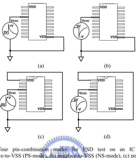
Fig. 1.1 The four pin-combination modes for ESD test on an IC product: (a) positive-to-VSS (PS-mode), (b) negative-to-VSS (NS-mode), (c) positive-to-VDD (PD-mode), and (d) negative-to-VDD (ND-mode).
Fig. 1.2 Typical on-chip ESD protection circuits in a CMOS IC.
Fig. 1.3 Typical circuit diagrams for (a) the traditional CMOS I/O buffer, and (b) the mixed-voltage I/O circuits with the stacked-nMOS and the N-well self-biased pMOS.
Fig. 1.4 The ESD current paths of (a) the traditional I/O pad with power-rail ESD clamp circuit, and (b) the mixed-voltage I/O pad with power-rail ESD clamp circuit, under the positive-to-VSS (PS-mode) ESD stress. The ESD current paths are indicated by the dashed lines.
Fig. 1.5 An example to show the power-down-mode operation issue on a system with two chips, which are biased with separated VDD1 and VDD2 power supplies.
Fig. 1.6 The typical ESD protection scheme for LCD driver ICs.
Fig. 1.7 (a) The system-level EMC/ESD test on LCD panel of notebook by an ESD gun. (b) The transient overshooting/ undershooting voltage waveform on the VDD pin of the driver ICs during system-level EMC/ESD test.
Fig. 1.8 (a) Layout view and (b) device structures of the traditional I/O cell with double guard rings inserted between input (or output) pMOS and nMOS devices.
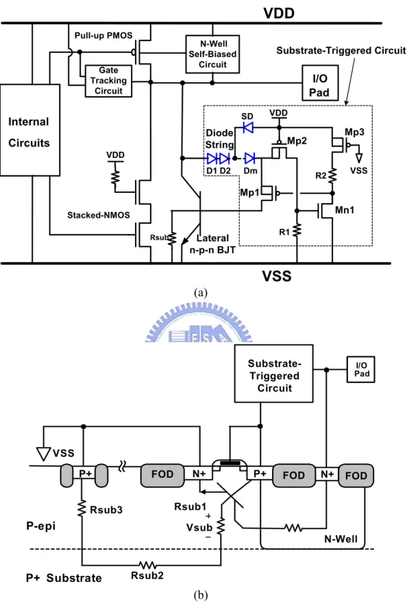
Fig. 1.9 (a) ESD protection design with substrate-triggered lateral n-p-n BJT device to protect the mixed-voltage I/O circuits. (b) Cross-sectional view of the lateral n-p-n BJT device in a thin-epi CMOS process.
Fig. 1.10 (a) ESD protection circuit with the SNTSCR device to protect the mixed-voltage I/O circuits. (b) Realizations of the SNTSCR device and the ESD detection circuit with the gate-coupling technique to trigger on the SNTSCR device.
Fig. 1.11 ESD protection design with the diode string connected between the I/O pad and VDD power line to protect the mixed-voltage I/O circuits. An additional snubber diode (SD) is used to reduce the leakage current of the diode string due to the Darlington amplification.
Fig. 1.13 The ESD protection network with the additional ESD bus line for the mixed-voltage I/O circuits. One power-rail ESD clamp circuit is connected between VDD power line and VSS power line. A second power-rail ESD clamp circuit is connected between ESD bus line and VSS power line.
Fig. 1.14 ESD protection design with low-voltage-triggered p-n-p (LVTPNP) device for the I/O interfaces with input voltage level higher than VDD or lower than VSS.
Fig. 1.15 High-voltage-tolerant ESD protection design with the forward-biased diode in series with one stacked nMOS for analog ESD protection to reduce the input parasitic capacitance.
CHAPTER 2
Fig. 2.1 (a) The finger-type layout pattern, and (b) the corresponding cross-sectional view, of the stacked-nMOS device for mixed-voltage I/O circuit in a p-substrate CMOS process.
Fig. 2.2 Comparisons of HBM ESD robustness of the stacked-nMOS device with or without the silicide-blocking process, under (a) different channel widths, and (b) different poly-to-poly spacings, of the stacked-nMOS device fabricated in a 0.25-µm CMOS process.
Fig. 2.3 (a) The finger-type layout pattern, and (b) the corresponding cross-sectional view, of the substrate-triggered stacked-nMOS device for mixed-voltage I/O circuit in a p-substrate CMOS process.
Fig. 2.4 The schematic circuit diagram of the substrate-triggered stacked-nMOS device with substrate-triggered circuit for the mixed-voltage I/O circuits.
Fig. 2.5 The cross-sectional view of the substrate-triggered stacked-nMOS device with substrate-triggered circuit for the mixed-voltage I/O circuits.
Fig. 2.6 The modified design of the substrate-triggered stacked-nMOS device with substrate-triggered circuit for the mixed-voltage I/O circuits without generating extra additional capacitance to the I/O pad.
Fig. 2.7 (a) The measured I-V characteristics of the substrate-triggered stacked-nMOS device with different substrate-triggered currents (Itrig). (b) The relation between the trigger voltage of the stacked-nMOS device and the substrate-triggered current (Itrig).
substrate-triggered currents.
Fig. 2.9 The dependence of It2 level on the substrate-triggered current (Itrig) under the different channel widths of substrate-triggered stacked-nMOS device.
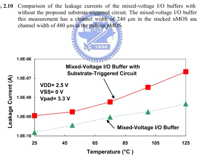
Fig. 2.10 Comparison of the leakage currents of the mixed-voltage I/O buffers with or without the proposed substrate-triggered circuit. The mixed-voltage I/O buffer in this measurement has a channel width of 240 µm in the stacked nMOS and a channel width of 480 µm in the pull-up pMOS.
Fig. 2.11 The leakage currents of the mixed-voltage I/O buffers with or without the substrate-triggered circuit under different temperatures.
Fig. 2.12 The positive-to-VSS (PS-mode) HBM ESD levels of the mixed-voltage I/O buffers with or without the substrate-triggered circuit, realized in a 0.25-µm CMOS process with silicide-blocking process.
CHAPTER 3
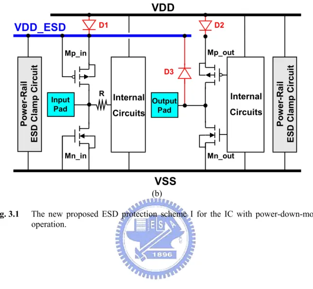
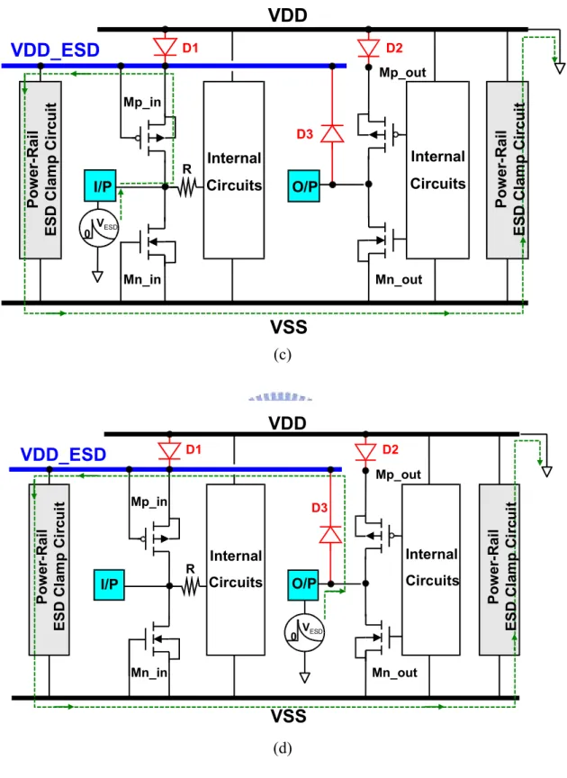
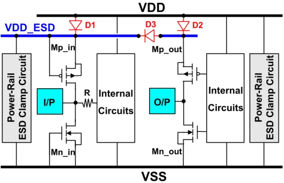
Fig. 3.1 The new proposed ESD protection scheme I for the IC with power-down-mode operation.
Fig. 3.2 The ESD current discharging paths of (a) the input pad under PS-mode ESD stress condition, (b) the output pad under PS-mode ESD stress condition, (c) the input pad under PD-mode ESD stress condition, and (d) the output pad under PD-mode ESD stress condition.
Fig. 3.3 The new proposed ESD protection scheme II for the IC with power-down-mode operation.
Fig. 3.4 The new proposed ESD protection scheme III for the IC with power-down-mode operation.
Fig. 3.5 The layout view of the new proposed ESD protection scheme I fabricated in a 0.35-µm silicided CMOS process.
Fig. 3.6 The circuit diagram of power-rail ESD clamp circuit.
Fig. 3.7 Comparison of the measured leakage currents at (a) the input pad under normal circuit operating condition, (b) the input pad under power-down-mode operating condition, and (c) the output pad under power-down-mode operating condition, of the traditional and new proposed ESD protection schemes.
circuit operating condition and power-down-mode operating condition.
Fig. 3.9 The measured voltage waveforms on the input/output pad of IC with the traditional ESD protection scheme under (a) normal circuit operating condition with VDD= 3.3V and VSS= 0V, and (b) power-down-mode operating condition with VDD= floating and VSS= 0V. (Y axis= 1V/Div., X axis= 200ns/Div.)
Fig. 3.10 The measured voltage waveforms on the input/output pad of IC with the proposed ESD protection scheme I under (a) normal circuit operating condition with VDD= 3.3V and VSS= 0V, and (b) power-down-mode operating condition with VDD= floating and VSS= 0V. (Y axis= 1V/Div., X axis= 200ns/Div.)
Fig. 3.11 (a) The output-swing improvement circuit connecting between the VDD power line and VDD_ESD bus line in the ESD protection scheme II. (b) The circuit diagram of output-swing improvement circuit.
Fig. 3.12 The measured leakage currents at I/O pads of new proposed ESD protection scheme II with the output-swing improvement circuit under normal circuit operating condition and power-down-mode operating condition.
Fig. 3.13 The measured voltage waveforms on the input/output pad of the proposed ESD protection scheme II with output-swing improvement circuit under (a) normal circuit operating condition with VDD= 3.3V and VSS= 0V, and (b) power-down-mode operating condition with VDD= floating and VSS= 0V. (Y axis= 1V/Div., X axis= 200ns/Div.)
CHAPTER 4
Fig. 4.1 The TLP-measured I-V characteristics of (a) DDD MOS structure fabricated in a 0.35-µm 18-V CMOS process and (b) LDMOS structure fabricated in a 0.25-µm 40-V CMOS process.
Fig. 4.2 Simulated current distributions in the 40-V nMOSFET under the (a) first snapback state, and (b) second snapback state.
Fig. 4.3 The (a) cross-sectional view, and (b) TLP-measured I-V characteristic, of high-voltage gate-grounded nMOS (GGNMOS) device fabricated in a 0.25-µm 40-V CMOS process.
Fig. 4.4 The (a) cross-sectional view, and (b) TLP-measured I-V characteristic, of high-voltage silicon controlled rectifier (SCR) device fabricated in a 0.25-µm
Fig. 4.5 The (a) cross-sectional view, and (b) TLP-measured I-V characteristic, of high-voltage field-oxide (FOD) device fabricated in a 0.25-µm 40-V CMOS process.
Fig. 4.6 The (a) cross-sectional view, and (b) TLP-measured I-V characteristic, of high-voltage gate-VDD pMOS (GDPMOS) device fabricated in a 0.25-µm 40-V CMOS process.
Fig. 4.7 The measurement setup for transient latchup (TLU) test.
Fig. 4.8 The measured voltage waveform on the high-voltage GGNMOS device under TLU test. (Y axis= 10 V/Div., X axis= 100 ns/Div.)
Fig. 4.9 The measured voltage waveform on the high-voltage SCR device under TLU test. (Y axis= 10 V/Div., X axis= 100 ns/Div.)
Fig. 4.10 The measured voltage waveforms on the high-voltage FOD device under TLU test with (a) positive charging voltage, and (b) negative charging voltage. (Y axis= 10 V/Div., X axis= 100 ns/Div.)
Fig. 4.11 (a) The measurement setup of single high-voltage FOD device and stacked-field-oxide structure under TLP stress. (b) The TLP-measured I-V characteristics of these devices with different device widths. W1 is the channel width of FOD1, and W2 is the channel width of FOD2.
Fig. 4.12 It2 currents of single FOD device and stacked-field-oxide structure as a function of device channel width.
Fig. 4.13 The TLP-measured I-V curves of the stacked-field-oxide structure with different substrate-triggered currents.
Fig. 4.14 The measured voltage waveforms on the stacked-field-oxide structure under TLU test with (a) positive charging voltage, and (b) negative charging voltage. (Y axis= 10 V/Div., X axis= 100 ns/Div.)
Fig. 4.15 The proposed power-rail ESD clamp circuits in high-voltage CMOS ICs with (a) two cascaded FOD devices, and (b) three cascaded FOD devices.
CHAPTER 5
Fig. 5.1 (a) Layout view and (b) device structures of the new proposed I/O cell with embedded SCR structure I. The anode and cathode of embedded SCR structure I are formed by inserting extra p+ diffusion in n-well and n+ diffusion in p-well,
Fig. 5.2 The ESD current discharging paths of I/O cell with embedded SCR structure I under (a) positive-to-VSS ESD stress condition, (b) positive-to-VDD ESD stress condition, (c) negative-to-VSS ESD stress condition, and (d) negative-to-VDD ESD stress condition.
Fig. 5.3 (a) Layout view and (b) device structures of new proposed I/O cell with embedded SCR structure II. The anode and cathode of embedded SCR structure II are directly formed by the source of input (or output) pMOS and the source of nMOS, respectively.
Fig. 5.4 The new proposed whole-chip ESD protection scheme with embedded SCR structure in each I/O cell. The substrate-triggered technique was realized by the RC-based ESD detection circuit.
Fig. 5.5 The measured dc I-V characteristics of the (a) embedded SCR structure I, and (b) embedded SCR structure II, in the I/O cells under different temperatures.
Fig. 5.6 The relation between the holding voltage of the embedded SCR structures and the operating temperature.
Fig. 5.7 The measured dc I-V characteristics of the (a) embedded SCR structure I, and (b) embedded SCR structure II, in the I/O cells under different substrate-triggered currents (Itrig).
Fig. 5.8 The measured dc I-V characteristics of (a) the parasitic SCR structure (path B) between I/O pad and VSS power line, and (b) the parasitic SCR structure (path D) between I/O pad and VDD power line, in the I/O cell with embedded SCR structure II under different substrate-triggered currents (Itrig).
Fig. 5.9 (a) The TLP-measured I-V curves of the I/O cells with embedded SCR structures I and II under positive VDD-to-VSS ESD stress with or without ESD detection circuit. (b) The enlarged view around the switching point of the measured curves for I/O cells with ESD detection circuit.
Fig. 5.10 The TLP-measured I-V curves of the input pad under positive-to-VSS ESD stress with or without embedded SCR structure, where the I/O nMOS and pMOS are silicide-blocking but the embedded SCR structures are fully silicided.
Fig. 5.11 The TLP-measured I-V curves of the input pad under positive-to-VSS ESD stress with or without silicide blocking on the input pMOS and nMOS devices, whereas the embedded SCR structures are fully silicided.
and II under negative-to-VSS ESD stress.
Fig. 5.13 The testchip to verify ESD robustness of the I/O cells with embedded SCR structures. The output buffer of pMOS (Mp_out) and nMOS (Mn_out) in output cell are individually controlled by the input cells.
Fig. 5.15 Measured voltage waveforms on the I/O pads triggered by a 0-to-4V voltage pulse with a rise time of 10ns for the (a) traditional I/O cells, and (b) new proposed I/O cells with embedded SCR structure II, under pin-to-pin ESD stress condition. (Y axis: 1 V/div., X axis: 40 ns/div.)
Fig. 5.14 (a) The failure location at the input nMOS device for the I/O cells with embedded SCR structure I under positive-to-VSS ESD stress. (b) The failure location at the input nMOS device for the I/O cells with embedded SCR structure II under negative-to-VSS ESD stress.
Fig. 5.15 Measured voltage waveforms on the I/O pads triggered by a 0-to-4V voltage pulse with a rise time of 10ns for the (a) traditional I/O cells, and (b) new proposed I/O cells with embedded SCR structure II, under pin-to-pin ESD stress condition. (Y axis: 1 V/div., X axis: 40 ns/div.)
CHAPTER 1
INTRODUCTION
1.1 Background
Electrostatic Discharge (ESD) has become the main reliability concern on semiconductor products, especially for the system-on-a-chip (SOC) implementation in nanoscale CMOS processes. The ESD specifications of commercial IC products are generally required to be higher than 2kV in human-body-model (HBM) [1] ESD stress. Therefore, on-chip ESD protection circuits have to be added between the input/output (I/O) pad and VDD/VSS to provide the desired ESD robustness in CMOS integrated circuits (ICs) [2]-[4]. ESD stresses on an I/O pad have four pin-combination modes: positive-to-VSS (PS-mode), negative-to-VSS (NS-mode), positive-to-VDD (PD-mode), and negative-to-VDD (ND-mode), as shown in Figs. 1.1(a) ~ 1.1(d), respectively. The typical design of on-chip ESD protection circuits in a CMOS IC is illustrated in Fig. 1.2. To avoid the unexpected ESD damage in the internal circuits of CMOS ICs [5]-[7], the turn-on-efficient power-rail ESD clamp circuit was placed between VDD and VSS power lines [8]. ESD current at the I/O pad under the PS-mode ESD stress can be discharged through the parasitic diode of pMOS from I/O pad to VDD, and then through the VDD-to-VSS ESD clamp circuit to ground. Consequently, the traditional I/O circuits cooperating with the VDD-to-VSS ESD clamp circuit can achieve a much higher ESD level [8].
1.1.1 Issue of Mixed-Voltage I/O Interface
To improve circuit operating speed and performance, the device dimension of MOSFET has been shrunk in the advanced CMOS ICs. With the scaled-down device dimension in advanced CMOS technology, the power supply voltage is also scaled down to reduce the power consumption and to meet the gate-oxide reliability. However, most microelectronic systems nowadays consist of mix semiconductor chips fabricated in different CMOS technologies. Therefore, the microelectronic systems often require the interfaces between
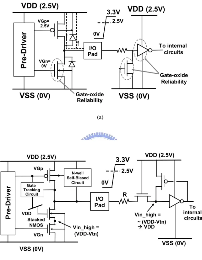
semiconductor chips or sub-systems which have different internal power supply voltages. With the different power supply voltages in a microelectronic system, chip-to-chip I/O interface circuits must be designed to avoid electrical overstress across the gate oxide [9], to avoid hot-carrier degradation [10] on the output devices, and to prevent the undesired leakage current paths between the chips [11], [12]. For example, a 3.3-V I/O interface is generally required by the ICs realized in CMOS processes with the normal internal power-supply voltage of 2.5V or 1.8V. The traditional CMOS I/O buffer with VDD of 2.5V is shown in Fig. 1.3(a) with both output and input stages. When an external 3.3-V signal is applied to the I/O pad, the channel of the output pMOS and the parasitic drain-to-well junction diode in the output pMOS cause the leakage current paths from the I/O pad to VDD, as the dashed lines shown in Fig. 1.3(a). Moreover, the gate oxides of the output nMOS, the gate-grounded nMOS for input electrostatic discharge (ESD) protection, and the input inverter stage are over-stressed by the 3.3-V input signal to suffer the gate-oxide reliability issue. By using the additional thick gate-oxide process (or called as dual gate-oxide CMOS process [13], [14]), the gate-oxide reliability issue can be avoided. However, the process complexity and fabrication cost are increased.
To solve the gate-oxide reliability issue without using the additional thick gate-oxide process, the stacked-MOS configuration has been widely used in the mixed-voltage I/O circuits [15]-[21]. The typical 2.5V/3.3V-tolerant mixed-voltage I/O circuit is shown in Fig. 1.3(b) [16]. The independent control on the top and bottom gates of stacked-nMOS device allows the devices to meet reliability limitations during normal circuit operation. The gate of top nMOS in the stacked-nMOS device is biased at VDD (e.g. 2.5V in a 2.5V/3.3V mixed-voltage I/O interface). The gate of bottom nMOS is biased at VSS by the pre-driver circuit to avoid leakage current through the stacked-nMOS structure, when the I/O circuit has a high-voltage input signal. With a high-voltage input signal at the pad (e.g. 3.3V in a 2.5V/3.3V mixed-voltage I/O interface), the common node between the top nMOS and bottom nMOS in the stacked-nMOS structure has approximately a voltage level of VDD-Vth (~ 1.9V), where Vth (~ 0.6V) is the threshold voltage of nMOS device. Therefore, the stacked-nMOS can be operated within the safe range for both dielectric and hot-carrier reliability limitations. The pull-up pMOS, connected from the I/O pad to the VDD power line, has the gate tracking circuits for tracking the gate voltage and the n-well self-biased circuits for tracking n-well voltage, which are designed to ensure that the pull-up pMOS does not
conduct current when the 3.3-V input signals enter the I/O pad. In such mixed-voltage I/O circuits, the on-chip ESD protection circuits will meet more design constraints and difficulty.
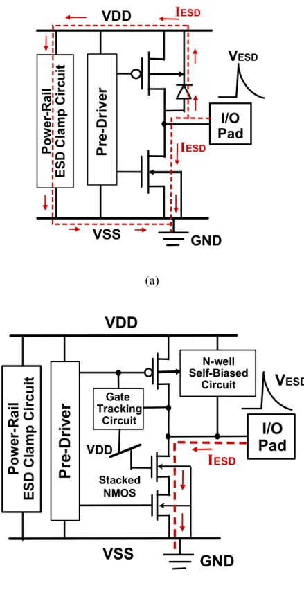
The ESD protection design of I/O pad cooperating with power-rail ESD clamp circuit is shown in Fig. 1.4(a), where a PS-mode ESD pulse is applied to the I/O pad. ESD current at the I/O pad under the PS-mode ESD stress can be discharged through the parasitic diode of pMOS from I/O pad to VDD and the VDD-to-VSS ESD clamp circuit to ground. But, due to the leakage current issue in the mixed-voltage I/O circuits, there is no diode connected from the I/O pad to VDD power line in the mixed-voltage I/O circuits. Without the diode connected from the I/O pad to VDD in the mixed-voltage I/O circuits, the ESD current at I/O pad under PS-mode ESD stress cannot be discharged from the I/O pad to VDD power line, and cannot be discharged through the additional VDD-to-VSS ESD clamp circuit. Therefore, the power-rail ESD clamp circuit did not help to pull up ESD level of the mixed-voltage I/O pad under the PS-mode ESD stress. The ESD current path in the mixed-voltage I/O circuits with power-rail ESD clamp circuit under PS-mode ESD stress in illustrated in Fig. 1.4(b). Such ESD current at the I/O pad is mainly discharged through the stacked-nMOS by snapback breakdown. However, the nMOS in stacked configuration has a higher trigger voltage and a higher snapback holding voltage, but a lower secondary breakdown current (It2), as compared to that of the single nMOS [22], [23]. Therefore, such mixed-voltage I/O circuits with stacked nMOS often have much lower ESD level for under PS-mode ESD stress, as compared to the traditional I/O circuits with a single nMOS [22]. In addition, without the diode connected from the I/O pad to VDD, the mixed-voltage I/O circuit also has a lower ESD level for I/O pad under PD-mode ESD stress. The absence of the diode between I/O pad and VDD power line in the mixed-voltage I/O circuits will seriously degrade ESD performance of the I/O pad under the PS-mode and PD-mode ESD stresses. By using extra process modification such as ESD implantation, the ESD robustness of stacked-nMOS device can be further improved [24], [25], but the process complexity and fabrication cost are increased. In addition, the induced high voltage on the gate of top nMOS transistor under ESD stress will cause high-current crowding effect in the channel region to seriously degrade ESD robustness of stacked-nMOS device in the mixed-voltage I/O circuits [26]. Therefore, effective ESD protection design without increasing process complexity is strongly requested by the mixed-voltage I/O circuits in the scaled-down CMOS processes. In this thesis, the substrate-triggered stacked-nMOS device, which combines the substrate-triggered technique with the stacked-nMOS device, is proposed to protect the mixed-voltage I/O circuits of
CMOS ICs [27].
1.1.2 Issue of Power-Down Application
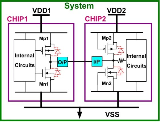
Nowadays power-down-mode feature plays an important role in portable and mobile SOC products that require effective power saving. In order to achieve IC power-down-mode operation, modifications on I/O circuits and ESD protection circuits have been studied [12], [28]. An example of two chips connected in an electronic system is shown in Fig. 1.5, where the output pad (O/P) of the chip_1 is connected to the input pad (I/P) of the chip_2. When the chip_2 goes into the power-down-mode operation, two situations are explained as follows. First, if VDD2 power line is grounded, a large leakage current may be induced from the input pad to the VDD2 power line through the parasitic diode of pMOS connected between the input pad and VDD2 power line, when the voltage level at the output pin of chip_1 is high. Second, if the VDD2 power line is floating, the internal circuits of chip_2 may be triggered to cause malfunction by charging the VDD2 power line through the parasitic diode of pMOS connected between the input pad and VDD2 power line, when the voltage level at the output pin of chip_1 is high. Therefore, the parasitic diode of pMOS connected between the input pad and VDD2 power line must be removed to avoid leakage current or malfunction, when the chip_2 goes into the power-down-mode operation in this typical example. In the traditional I/O circuits, ESD current at the I/O pad under the PS-mode ESD stress can be discharged through the parasitic diode of pMOS from I/O pad to VDD, and then through the VDD-to-VSS ESD clamp circuit to ground. However, the absence of the diode between I/O pad and VDD power line for power-down-mode application will seriously degrade ESD performance of the I/O pad under the PS-mode and PD-mode ESD stresses. To solve the ESD protection and leakage issue for IC with power-down-mode operation, some modified designs have also been reported [29], [30]. The gate-grounded nMOS has been used to replace the diode between the I/O pad and VDD power line [29]. In [30], the design was focused on improving the ESD robustness of the ESD protection circuit between the I/O pad and VSS power line. However, the turn-on efficiency of the ESD protection device [29] or the complicated ESD protection circuit [30] is the concern to implement the approach. In this thesis, three new ESD protection designs for IC with power-down-mode operation [31]-[33] are proposed. The new proposed designs can overcome the leakage issue and have a very high ESD level for IC with power-down-mode operation.
1.1.3 Issue of High-Voltage CMOS ICs
High-voltage transistors in smart power technologies have been extensively used for display driver ICs, power supplies, power management, and automotive electronics. The ESD reliability is an important issue for high-voltage transistors with applications in these products. In smart power technology, high-voltage MOSFET, silicon-controlled rectifier (SCR) device, and bipolar junction transistor (BJT) have been used as on-chip ESD protection devices [34]-[39]. Those earlier works focused on analyzing and improving ESD robustness of the ESD protection devices in high-voltage CMOS processes [34]-[39]. However, the latchup or latchup-like failure from such ESD protection devices under normal circuit operating condition was not considered, especially while the devices are used in the power-rail ESD clamp circuit. Fig. 1.6 shows the typical ESD protection scheme for LCD driver ICs (typically, gate driver with 40V, and source driver with 12V, for 14.1-inch notebook LCD panel). The output buffers (Mp and Mn) are controlled by the input control circuits through the level-shifter circuits. The diodes D1~D4 are used as on-chip ESD protection devices for input and output pads. The ESD current at the output pad under positive-to-VSS ESD stress can be discharged through the diode D1 to the VDD_HV power line, and then through the power-rail ESD clamp circuit from the VDD_HV power line to the grounded VSS power line, as the dashed line shown in Fig. 1.6. When the ESD protection device is used in the power-rail ESD clamp circuit, the device is expected to be kept off in normal circuit operating condition. During ESD stress conditions, the ESD protection device should be triggered on to discharge ESD current. If the holding voltage of the ESD protection device in power-rail ESD clamp circuit is smaller than the power supply voltage, the ESD device may be triggered on by the system-level electromagnetic compatibility (EMC)/ESD transient pulses to cause a very serious “latchup” or “latchup-like” failure in CMOS ICs. This phenomenon often leads to IC function failure or even destruction by burning out [40], [41]. The system-level EMC/ESD reliability of LCD panel has been requested up to 20kV of ESD stress in the air-discharge mode. The system-level EMC/ESD test on LCD panel of notebook by an ESD gun (Standard IEC 61000-4-2 [42]) is shown in Fig. 1.7(a). During the system-level ESD stress, the power lines of driver ICs in the LCD panel of notebook can be coupled with an overshooting/undershooting voltage up to several hundred volts [43], as that shown in Fig. 1.7(b). Especially, the driver ICs with tape carrier package (TCP) are directly attached to the LCD panel. No room is available for the driver ICs with on-board de-coupling
the transient voltage seen by the circuits in the driver ICs is quite large during such system-level EMC/ESD zapping. In this thesis, the holding voltage of the high-voltage devices in snapback breakdown condition has been found to be much smaller than the power supply voltage [44]-[46]. Such characteristics will cause the high-voltage CMOS ICs susceptible to the latchup or latchup-like danger in the practical system applications, especially while these devices are used in the power-rail ESD clamp circuit. Furthermore, a new latchup-free power-rail ESD clamp circuit in high-voltage CMOS process [45], [46] is proposed in this thesis.
1.1.4 Issue of Nanoscale CMOS Technology
To provide efficient ESD protection for CMOS ICs, the on-chip ESD protection circuits have to be designed and placed around the input, output, and power pads. In Fig. 1.2, the pMOS and nMOS are used as on-chip ESD protection devices for input and output pads. ESD current at the I/O pad under the PS-mode ESD stress can be discharged through the parasitic diode of pMOS from I/O pad to VDD, and then through the VDD-to-VSS ESD clamp circuit to ground. However, due to the parasitic resistance and capacitance along the VDD and VSS power lines, ESD protection efficiency is dependent on the pin location in a chip. To quickly bypass the ESD current during ESD-stress condition, the efficient VDD-to-VSS ESD clamp circuits are repeatedly inserted between VDD and VSS power lines in the appropriate distance to provide a low-impedance path between the VDD and VSS power lines [8]. Therefore, how to realize the area-efficient and turn-on-efficient power-rail ESD clamp circuits will be an important challenge to SOC applications with a much larger chip size but a reduced cell pitch for I/O cell. For CMOS IC applications, SCR can be a great candidate for on-chip ESD protection due to its highest ESD robustness, smallest layout area, and excellent clamping capabilities (low holding voltage and small turn-on resistance) [47]-[50], which can even provide efficient ESD protection to the ultra-thin gate oxide in nanoscale CMOS process [51]. However, SCR device was susceptible to latchup danger under normal circuit operating condition [52]. Because of the low holding voltage, such SCR devices could be accidentally triggered on by the noise pulses, when ICs are in normal circuit operating conditions. In the traditional I/O cells, double guard rings have been often inserted between input (or output) pMOS and nMOS devices to avoid the latchup issue [53]. The layout view and device structures of the traditional I/O cell are shown in Figs. 1.8(a) and 1.8(b), respectively.
supply voltage is also scaled down to meet the circuit requirement and gate-oxide reliability. The maximum supply voltage is only 1.2V in a 130-nm CMOS technology with the thin gate oxide of 20Å. If the holding voltage of parasitic SCR device is greater than the power supply voltage, latchup issue will not occur in such nanoscale CMOS process. Therefore, the SCR or parasitic SCR device can be used as on-chip ESD protection device without latchup concern in nanoscale CMOS process. A new ESD protection design for I/O cells with embedded SCR structure as power-rail ESD clamp device is proposed for nanoscale CMOS process [54], [55] in this thesis. Whole-chip ESD protection scheme can be successfully achieved within a small silicon area of I/O cell by this design.
1.2 ESD Protection Designs for Mixed-Voltage I/O Interfaces
1.2.1 Substrate-Triggered Stacked-NMOS Device
To improve the turn-on uniformity among the multiple fingers of CMOS output buffer, the substrate-triggered designs [56]-[58] have been reported to increase ESD robustness of the large-device-dimension nMOS. With the substrate-triggered technique, the substrate-triggered stacked-nMOS device [27] for mixed-voltage I/O interfaces is proposed and verified in Chapter 2 in this thesis. The ESD robustness of mixed-voltage I/O circuits can be effectively improved by this design without occupying extra silicon area to realize the additional stand-alone ESD protection device into the I/O cells.
1.2.2 Extra ESD Device between I/O pad and VSS
To improve ESD level of the mixed-voltage I/O circuits, the extra ESD device was added between I/O pad and VSS power line [59], [60]. The ESD current at the I/O pad under PS-mode ESD stress is designed to be directly discharged through this additional ESD device to the grounded VSS. The ESD current at the I/O pad under the PD-mode ESD stress can be discharged through this ESD device to VSS power line, and then through the parasitic diode of power-rail ESD clamp circuit to the grounded VDD.
One ESD protection design with the additional substrate-triggered lateral n-p-n BJT device has been used to protect the mixed-voltage I/O circuits in a fully salicided, 0.35-µm, thin-epi CMOS process [59]. The ESD protection design with substrate-triggered circuit and
the lateral n-p-n BJT device for the mixed-voltage I/O circuits is re-drawn in Fig. 1.9(a). The substrate-triggered circuit should meet the design constraints for providing effective ESD protection to the mixed-voltage I/O circuits, but without suffering the gate-oxide reliability issue. In this design, the substrate-triggered circuit is mainly composed of the diode string and a pMOS Mp1 to provide the substrate current for triggering on the lateral n-p-n BJT during ESD stress. A positive feedback network is formed with Mp2, Mn1, and R1, which maintains Mp1 in a highly conductive state to provide the substrate current during ESD stress. Moreover, to improve the turn-on efficiency of lateral n-p-n BJT device in a thin-epi CMOS process with much smaller substrate resistance (Rsub), the device structure of lateral n-p-n BJT is specifically designed in Fig. 1.9(b). The lateral n-p-n BJT device consists of an n+ diffusion (emitter), an n-well (collector), and a p+ diffusion as its base. A dummy gate is formed between the p+ base and n+ emitter regions. The collector n-well encloses a portion of the p+ base region. In this design, the HBM ESD level of the mixed-voltage I/O circuits has been verified greater than 2kV in a fully-salicided thin-epi CMOS process.
Another ESD protection design, by using the additional stacked-nMOS triggered silicon controlled rectifier (SNTSCR), has been reported to protect the mixed-voltage I/O circuits [60]. The ESD protection design with the additional SNTSCR device for protecting the mixed-voltage I/O circuits is shown in Fig. 1.10(a). The device structure of SNTSCR and the corresponding ESD detection circuit are shown in Fig. 1.10(b). The ESD detection circuit, designed by using the gate-coupled technique with consideration of the gate-oxide reliability issue, is used to provide suitable gate bias to trigger on the SNTSCR device under ESD stress condition. On the contrary, this ESD detection circuit must keep the SNTSCR off when the IC is under normal circuit operating condition. During normal circuit operating condition, the Mn3 in Fig. 1.10(b) acts as a resistor to bias the gate voltage (Vg1) of Mn1 at VDD. But, the gate of Mn2 is grounded through the resistor R2 and Mn4. So, all the devices in the ESD protection circuit can meet the electrical-field constraint of gate-oxide reliability under normal circuit operating condition. Under PS-mode ESD stress condition, the Mp1 is turned on but Mn3 is off since the initial voltage level on the floating VDD line is ~0V. The capacitors C1 and C2 are designed to couple ESD transient voltage from the I/O pad to the gates of Mn1 and Mn2, respectively. The coupled voltage should be designed greater than the threshold voltage of nMOS to turn on Mn1 and Mn2 for triggering on the SNTSCR device, before the devices in the mixed-voltage I/O circuit are damaged by ESD stress. With the gate-coupled circuit technique, the trigger voltage of SNTSCR can be significantly reduced,
so the SNTSCR can be quickly triggered on to discharge ESD current. By changing the connection of the ESD protection circuit from the I/O pad to the floating n-well of the pull-up pMOS in the mixed-voltage I/O circuit, the SNTSCR device can have a high enough noise margin to the overshooting glitch on the I/O pad, during the normal circuit operating condition. From the experimental results in a 0.35-µm CMOS process, the HBM ESD level of the mixed-voltage I/O circuits with this ESD protection design has been greatly improved up to 8kV, as compared with that (~2kV) of the original mixed-voltage I/O circuits with only stacked nMOS device.
1.2.3 Extra ESD Device between I/O pad and VDD
To improve ESD level of the mixed-voltage I/O circuits, the extra ESD device was added between I/O pad and VDD power line [61]-[63]. The ESD current at the I/O pad under PS-mode ESD stress is designed to be discharged through this additional ESD device to VDD power line, and then through the power-rail ESD clamp circuit to the grounded VSS. The ESD current at the I/O pad under the PD-mode ESD stress can be directly discharged through this additional ESD device to the grounded VDD.
Because the diode in forward-biased condition can sustain much higher ESD current, the diode string has been used for protecting the mixed-voltage I/O circuits [61], [62], or used to realize the power-rail ESD clamp circuit [64]. The ESD protection design with the diode string connected between the I/O pad and VDD power line for the mixed-voltage I/O circuits is shown in Fig. 1.11. The number of diodes in the diode string is determined by the voltage difference between the maximum input voltage at I/O pad and the VDD supply voltage. To reduce the turn-on resistance from I/O pad to VDD during ESD stress, the area of such diodes has to be scaled up by the number of the diodes in stacked configuration. The major concern of using the diode string for ESD protection in the mixed-voltage I/O circuits is the leakage current. While the mixed-voltage I/O circuit is operating at a high-temperature environment with a high-voltage input signal, the forward-biased leakage current from the I/O pad to VDD through the stacked diodes could trigger on the parasitic vertical p-n-p BJT devices in the diode string. The Darlington bipolar amplification of these parasitic p-n-p BJT devices in the diode string will induce a large leakage current into the substrate. In Fig. 1.11, an additional snubber diode (SD) was used to reduce the leakage current due to the Darlington bipolar amplification in the diode string [61], [62].
device connected between I/O pad and VDD, has been designed to protect the mixed-voltage I/O circuits [63], as that shown in Fig. 1.12. In this ESD protection design, the pMOS Mp1 acting as ESD clamp device should be kept off to avoid the leakage current path during normal circuit operating condition. Under PD-mode ESD stress condition, the parasitic lateral p-n-p BJT in the device structure of Mp1 is turned on to discharge ESD current. In the 3.6V/5V mixed-voltage IC application, when the input voltage at I/O pad is 0V, the n-well voltage and gate voltage of Mp1 is clamped at VDD (3.6V) through the turn-on of Mp2 and Mp4. When the input voltage at I/O pad is 5V, the n-well voltage of Mp1 is maintained at 5-Vd (where Vd is the cut-in voltage of the parasitic drain-to-well diode), and the gate voltage of Mp1 is clamped at 5V through the turn-on of Mp3. Therefore, this design can meet the gate-oxide reliability constraints without leakage current path from I/O pad to VDD during normal circuit operating condition. Under ESD stress condition, the parasitic lateral p-n-p BJT in Mp1 is turned on to discharge ESD current by avalanche breakdown. Such a gated p-n-p BJT should be designed to effectively clamp the overstress ESD pulse without causing ESD damage in the mixed-voltage I/O circuits.
1.2.4 ESD Protection Design with ESD Bus
The whole-chip ESD protection scheme by using the additional ESD bus for the IC with power-down-mode application is proposed in Chapter 3 in this thesis [31]-[33]. Such design concept with ESD bus can be used to form the ESD protection network for the mixed-voltage I/O circuits, as shown in Fig. 1.13. The additional ESD bus line is realized by a wide metal line in CMOS IC [65]. The ESD bus is not directly connected to an external power pin, but biased to VDD through the diode D1 in Fig. 1.13. The diode D1 connected between the VDD power line and ESD bus is also used to block the leakage current path from the I/O pad to VDD during normal circuit operating condition with a high-voltage input signal. The diode Dp is connected between I/O pad and ESD bus, whereas the diode Dn is connected between VSS power line and I/O pad. One (the first) power-rail ESD clamp circuit is connected between VDD power line and VSS power line. Another (the second) power-rail ESD clamp circuit is connected between the ESD bus and VSS power line. The second power-rail ESD clamp circuit connected between ESD bus and VSS power line should be designed with high-voltage-tolerant constraints without suffering the gate-oxide reliability issue. The ESD current at the I/O pad under PS-mode ESD stress can be discharged through the diode Dp to
The ESD current at the I/O pad under the PD-mode ESD stress can be discharged through the diode Dp to the ESD bus, the second power-rail ESD clamp circuit to VSS power line, and then through the parasitic diode of the first power-rail ESD clamp circuit to the grounded VDD. With the turn-on-efficient power-rail ESD clamp circuits, high ESD level for the mixed-voltage I/O circuits can be achieved by this ESD protection scheme with ESD bus.
1.2.5 Special Applications
One of the mixed-voltage circuit applications, such as the interface in ADSL, has the input signals with voltage level higher than VDD and lower than VSS. This application limits the ESD diodes connected between the input pad and VDD/VSS power lines. To meet such mixed-voltage I/O interface, the SCR device with floating p-well structure in an n-substrate CMOS process has been used as on-chip ESD protection device [66]. However, the SCR device with a floating well structure is very sensitive to latchup [53], [67]. The mixed-voltage I/O interfaces in the system applications often meet serious overshooting or undershooting signal transition, which could trigger on the SCR device in the ESD protection circuit of I/O pad to induce latchup troubles to the chip [66]. A new ESD protection design, by using the low-voltage-triggered p-n-p (LVTPNP) device, has been proposed to protect such I/O interfaces with input voltage level higher than VDD and lower than VSS [68], as shown in Fig. 1.14. Comparing to the traditional p-n-p device in CMOS process, the LVTPNP device with a lower breakdown voltage by avalanche breakdown across the p+/n-well or n+/p-sub junctions provides effective discharging path to protect the mixed-voltage I/O interfaces against ESD stresses. During normal circuit operation condition, the LVTPNP device is kept off without causing any leakage current path. In cooperating with the power-rail ESD clamp circuit, the ESD current is discharged through the LVTPNP device by avalanche breakdown under four modes of ESD stresses. The ESD robustness of the LVTPNP device can be further improved by layout optimization.
For high-frequency and analog circuit applications, the high-voltage-tolerant ESD protection design should meet the constraint of low parasitic capacitance. The traditional analog ESD protection with double diodes connected between I/O pad and VDD/VSS power lines [69] cannot meet the high-voltage tolerant requirement. A high-voltage-tolerant ESD protection design, by using the forward-biased diode in series with the stacked-nMOS device, has been reported for analog ESD protection to reduce the input parasitic capacitance [70], as
junction capacitance of D1 plus the junction capacitance of D2. The diodes D1 and D2 can be drawn with small layout area, because the ESD current is discharged through these diodes under forward-biased condition. Therefore, the total parasitic input capacitance seen by the analog pin was reduced. The gates of Mn1 and Mn3 are connected to VDD to meet the gate-oxide reliability. The gates of Mn2 and Mn4 are grounded by the dynamic-floating-gate technique [71] to improve turn-on uniformity among the multiple fingers of the stacked nMOS device. The ESD current at the I/O pad under PS-mode ESD stress can be discharged through the diode D1 and the parasitic n-p-n BJT of stacked nMOS (Mn3 and Mn4) to the grounded VSS. The ESD current at the I/O pad under PD-mode ESD stress can be discharged through the diode D1 and the parasitic n-p-n BJT of stacked nMOS (Mn1 and Mn2) to the grounded VDD. Because the ESD current is discharged through the stacked-nMOS device by snapback breakdown in this design, the turn-on efficiency and ESD robustness of stacked-nMOS devices (Mn1 ~ Mn4) need to be further improved by the additional ESD-implantation process [72].
1.3 Thesis Organization
To overcome the ESD design constraints in mixed-voltage I/O interfaces, power-down-mode application, high-voltage CMOS process, and nanoscale CMOS technology, the novel on-chip ESD protection circuits are developed and verified in this thesis. This thesis contains six chapters. Chapter 1 presents an overview on the design concept and circuit implementations of the ESD protection designs for mixed-voltage I/O interfaces without using the additional thick gate-oxide process. To improve ESD level of the mixed-voltage I/O circuits, the ESD protection design without increasing the process complexity is strongly requested by the mixed-voltage I/O circuits in consumer IC products. Such ESD protection design in the mixed-voltage I/O circuits still meets the gate-oxide reliability constraints, and needs to prevent the undesired leakage current paths during normal circuit operating condition. Under ESD stress condition, the ESD protection circuit should be quickly triggered on to discharge ESD current.
In chapter 2, the substrate-triggered stacked-nMOS device, which combines the substrate-triggered technique with the stacked-nMOS device, is proposed to protect the mixed-voltage I/O circuits of CMOS ICs. The proposed ESD protection circuit with the
substrate-triggered technique is fully compatible to general CMOS process without causing the gate-oxide reliability problem. Without using the thick gate oxide, the new proposed design has been fabricated and verified for 2.5V/3.3V tolerant mixed-voltage I/O circuit in a 0.25-µm salicided CMOS process. The HBM ESD level of the mixed-voltage I/O buffer can be improved from the original 3.4kV up to 5.6kV by the substrate-triggered circuit. By using this substrate-triggered design, the ESD robustness of mixed-voltage I/O circuits can be effectively improved without occupying extra silicon area to realize the additional stand-alone ESD protection device into the I/O cells.
In chapter 3, three new ESD protection designs for CMOS IC with power-down-mode operation are proposed. By using the additional ESD bus and diodes, the ESD protection design can block the leakage current from I/O pin to VDD and avoid the malfunction during power-down-mode operating condition. During normal circuit operating condition, the ESD protection design has no leakage path to interfere with the normal circuit functions. The whole-chip ESD protection design can be achieved by insertion of ESD clamp circuits between VSS power line and both VDD power line and ESD bus. Experimental results have verified that the HBM ESD level of the new proposed designs can be greater than 7.5kV in a 0.35-µm silicided CMOS process. Furthermore, output-swing improvement circuit is proposed to achieve the full swing of output voltage level during normal circuit operating condition.
In chapter 4, the double snapback characteristic in the high-voltage nMOSFETs has been found and analyzed. Furthermore, the holding voltage of the high-voltage devices in snapback breakdown condition has been found to be much smaller than the power supply voltage. Such characteristic will cause the high-voltage CMOS ICs susceptible to the latchup or latchup-like danger in the practical system applications, especially while these devices are used in the power-rail ESD clamp circuit. A new latchup-free design on the power-rail ESD clamp circuit with stacked-field-oxide structure is proposed and successfully verified in a 0.25-µm 40-V CMOS process to achieve the desired ESD level. The total holding voltage of the stacked-field-oxide structure in snapback breakdown condition can be larger than the power supply voltage. Therefore, latchup or latchup-like issues can be avoided by stacked-field-oxide structures for the IC applications with power supply of 40V.
In chapter 5, a new ESD protection design for I/O cells with embedded SCR structure as power-rail ESD clamp device in a 130-nm CMOS process is proposed. Two new embedded SCR structures without latchup danger are proposed to be placed between the input (or output)
pMOS and nMOS devices of the I/O cells. Furthermore, the turn-on efficiency of embedded SCR can be significantly increased by substrate-triggered technique. Experimental results have verified that the HBM ESD level of this new proposed I/O cells can be greater than 5kV in a 130-nm fully salicided CMOS process. By including the efficient power-rail ESD clamp device into each I/O cell, whole-chip ESD protection scheme can be successfully achieved within a small silicon area of I/O cell.
Finally, the main results of this thesis are summarized in chapter 6. Some suggestions for the future works are also addressed in this chapter.
VDD VSS 0V VESD +V VDD VSS 0V VESD -V (a) (b) VDD VSS 0V VESD +V VDD VSS 0V VESD -V (c) (d)
Fig. 1.1 The four pin-combination modes for ESD test on an IC product: (a) positive-to-VSS (PS-mode), (b) negative-to-VSS (NS-mode), (c) positive-to-VDD (PD-mode), and (d) negative-to-VDD (ND-mode).
Internal Circuits Internal Circuits Po w er -R ail E S D Cl am p C ircui t Input Pad
VDD
VSS
Mp_in Mp_out Mn_in Mn_out Output Pad RI/O Pad
VDD
(2.5V)
VSS
(0V)
Pre-D
riv
er
VGp= 2.5V VGn= 0V To internal circuitsVDD
(2.5V)
VSS
(0V)
0V3.3V
2.5V Gate-oxide Reliability Gate-oxide Reliability (a) I/O Pad VDD (2.5V) VSS (0V)Pre-D
ri
ve
r
VGp VGn To internal circuits VDD (2.5V) VSS (0V) 0V3.3V
2.5V R Vin_high = ~ (VDD-Vtn) ÆVDD VDD N-well Self-Biased Circuit Stacked NMOS Vin_high = (VDD-Vtn) Gate Tracking Circuit (b)Fig. 1.3 Typical circuit diagrams for (a) the traditional CMOS I/O buffer, and (b) the
mixed-voltage I/O circuits with the stacked-nMOS and the N-well self-biased pMOS.