國
立 交 通 大 學
電子工程學系
電子研究所
博
士 論 文
高介電常數氧化鐠閘極介電層與新穎結構
於複晶矽薄膜電晶體之研究
Study on High-
κ Pr
2
O
3
Gate Dielectric and
Novel Structures of Polycrystalline
Silicon Thin-Film Transistors
研 究 生:張 家 文
指導教授:雷 添 福 博士
中華民國 九十七 年 五 月
高介電常數氧化鐠閘極介電層與新穎結構
於複晶矽薄膜電晶體之研究
Study on High-
κ Pr
2
O
3
Gate Dielectric and
Novel Structures of Polycrystalline Silicon
Thin-Film Transistors
研 究 生:張家文 Student:Chia-Wen Chang
指導教授:雷添福 博士
Advisor:Dr. Tan-Fu Lei
國立交通大學
電子工程學系 電子研究所
博士論文
A Dissertation
Submitted to Department of Electronics Engineering
and Institute of Electronics
College of Electrical and Computer Engineering
National Chiao Tung University
In Partial Fulfillment of the Requirements
For the Degree of
Doctor of Philosophy
in Electronics Engineering
May 2008
Hsinchu, Taiwan, Republic of China
高介電常數氧化鐠閘極介電層與新穎結構
於複晶矽薄膜電晶體之研究
學生: 張
家 文
指導教授: 雷
添 福 博士
國立交通大學
電子工程學系
電子研究所博士班
摘
要
此論文提出多種有效方式來改善複晶矽薄膜電晶體的電性,首先,提出具有高介 電常數氧化鐠閘極介電層之固相再結晶複晶矽薄膜電晶體。此外,深入探討應用兩種 氟鈍化技術包括氟離子佈值及四氟化碳電漿處理以製備高效能及高可靠度之複晶矽氧 化鐠薄膜電晶體。並研究兩種複晶矽晶粒尺寸增大技術於固相再結晶複晶矽薄膜電晶 體之應用。最後,發展一個簡單的側壁邊襯技術來製作具有奈米線通道之固相結晶和 金屬誘發側向結晶複晶矽薄膜電晶體。 首先,整合氮化鈦金屬閘極和高介電常數氧化鐠閘極介電層來發展高效能之固相 再結晶複晶矽薄膜電晶體。應用氧化鐠閘極介電層可得到薄的等效氧化層厚度和高的 閘極電容密度並且可以使複晶矽通道區域誘發產生更大量的可移動載子。因此,複晶 矽薄膜裡的晶粒邊界缺陷態位會被大量誘導產生的載子迅速的填滿,可以大幅的改善 次臨界斜率。即使在沒有額外施加氫化處理製程或採用先進的相結晶技術之下,複晶矽氧化鐠閘極介電層薄膜電晶體的電性明顯地勝過傳統的複晶矽氧化矽閘極介電層薄 膜電晶體。 接著,我們應用兩種氟鈍化技術包括氟離子佈值及四氟化碳電漿處理於複晶矽氧 化鐠閘極介電層薄膜電晶體。這些氟鈍化技術可將氟原子引進複晶矽薄膜中及氧化鐠 閘極介電極/複晶矽通道界面處來修補晶粒邊界缺陷態位。因此,藉著摻雜氟原子進入 複晶矽薄膜中,複晶矽氧化鐠閘極介電層薄膜電晶體的元件電性以及臨界電壓下降特 性可大幅的改善,尤其是針對關閉狀態的漏電流改善更加顯著。此外,這些氟鈍化技 術也可形成強的矽-氟鍵結以取代一般弱的矽-矽鍵結以及矽-氫鍵結,以增進熱載子應 力的免疫力。 其次,我們發展出兩種具有表面成核固相再結晶方式之複晶矽晶粒尺寸增大技 術,其中包括氬離子佈植於非晶矽/下層氧化矽界面處以及新穎的懸浮通道結構。在界 面處的大量矽晶粒成核機制可被有效抑制住,而成核機制會選擇由較少成核點的非晶 矽自由表面處開始,在較少的矽晶粒成核點情況下可以得到較好的複晶矽晶粒特性包 含較大晶粒尺寸及較少結構缺陷。因此,利用這些晶粒尺寸增大技術可以顯著的改善 複晶矽薄膜電晶體的電性。 在論文的最後,我們發展出利用簡單的側壁邊襯技術且不需要先進的微影製程來 形成自我對準的50 奈米線寬的奈米線通道。探討應用固相再結晶和金屬誘發側向再結 晶技術於複晶矽奈米線通道薄膜電晶體的應用。由於固相再結晶複晶矽奈米線通道薄 膜電晶體具有三維之類三閘極結構,邊際電場會誘導側壁及角落產生額外的電流貢獻 效應以增進閘極對奈米線通道的控制能力。另一方面,金屬誘發側向再結晶複晶矽奈 米線通道薄膜電晶體具有較佳的複晶矽晶粒特性,因此具有較好的導通特性以及較低 的關閉狀態漏電流。
Study on High-
κ Pr
2O
3Gate Dielectric and Novel
Structures of Polycrystalline Silicon Thin-Film Transistors
Student: Chia-Wen Chang
Advisor: Dr. Tan-Fu Lei
Department of Electronics Engineering &
Institute of Electronics
National Chiao Tung University
ABSTRACT
In this thesis, several effective ways were proposed to improve the electrical performances of polycrystalline silicon thin-film transistors (poly-Si TFTs). First, solid-phase crystallized (SPC) poly-Si TFTs with high-κ Pr2O3 gate dielectric were proposed. In addition,
applying two kinds of fluorination techniques including fluorine ion implantation and CF4
plasma treatments to the SPC poly-Si Pr2O3 TFTs were deeply investigated. Besides, SPC
poly-Si TFTs with two poly-Si grain-size enlargement techniques were demonstrated and characterized. Finally, a simple sidewall spacer technique was developed to fabricate SPC and metal-induced lateral crystallized (MILC) poly-Si TFTs with NW channels.
First, high-performance SPC poly-Si TFTs integrated with TiN metal gate and high-κ Pr2O3 gate dielectric have been demonstrated. Using the Pr2O3 gate dielectric can obtain thin
equivalent-oxide thickness and high gate capacitance density, and then induce much more mobile carriers in the poly-Si channel region. Hence, the grain-boundary trap states in the poly-Si films could be quickly filled up by the large amount of induced carriers to improve the subthreshold swing. The electrical characteristics of the poly-Si Pr2O3 gate dielectric
dielectric TFTs even without additional hydrogenation treatments or advanced phase crystallization techniques.
Then, we have incorporated two kinds of fluorination techniques including fluorine ion implantation and CF4 plasma treatments into the poly-Si Pr2O3 gate dielectric TFTs.
Utilizing these fluorination techniques, fluorine atoms can be introduced into the poly-Si films and the Pr2O3 gate dielectric/poly-Si channel interface to passivate the grain-boundary
trap states. Hence, the electrical performances and threshold-voltage rolloff properties of the poly-Si Pr2O3 gate dielectric TFTs can be significantly improved by the incorporation of
fluorine atoms, in particular, a more obvious enhancement on the decreasing of the off-state leakage currents. Besides, these fluorination techniques also enhance the immunity against hot-carrier stress, due to the formation of strong Si-F bonds in place of weak Si-Si and Si-H bonds.
Next, we have developed two kinds of poly-Si grain-size enhancement techniques associating with surface-nucleation SPC scheme including deep Argon ion implantation into the α-Si/underlying SiO2 interface and novel floating-channel structure. The silicon grain
nucleation at the interface is effectively suppressed, and then the nucleation process with fewer nucleation sites will initiate on the α-Si free surface. Fewer silicon grain nucleation results in better poly-Si grain crystallinity with larger grain size and fewer microstructural defects. The electrical characteristics of the poly-Si TFTs are greatly improved by introducing these poly-Si grain-size enhancement techniques.
Finally, we demonstrate a simple sidewall spacer technique for forming self-aligned 50-nm line-width nanowire (NW) channels without any advanced lithography process. Poly-Si TFTs with NW channels crystallized by SPC and metal-induced lateral crystallization (MILC) techniques are investigated. The SPC poly-Si NW TFTs have excellent gate controllability over the NW channels due to the three-dimensional (3-D) tri-gate-like structure with the sidewall and corner contribution effects. On the other hand, the MILC poly-Si NW TFTs exhibit better turn-on characteristics and lower off-state leakage currents due to the superior poly-Si grain crystallinity.
誌 謝
本論文能夠順利完成,要感謝的人實在太多了!沒有眾人的支持與鼓勵,就無法 成就這一切。首先我要向我的指導教授−雷添福博士致上最高的敬意。感謝雷老師在這 四年的博士生涯中給予學業研究的鼓勵與支持,尤其是在實驗研究與生活上遭遇困難 時,雷老師的關懷總是能讓學生產生明確的研究態度與方法,讓我在半導體領域中更 為精進,並深深影響我的待人處世態度,令我獲益良多。 感謝曾經指導過我的學長,李名鎮學長、李宗霖學長、王哲麒學長、游信強學長、 謝明山學長、林育賢學長、王獻德學長、郭柏儀學長、陳建豪學長、楊紹明學長、謝 德慶學長、李美錡學姐、賴久盟學長、謝松齡學長、羅韋翔學長、林余俊學長和江國 誠學長,從你們身上學到做實驗的認真態度。感謝鄧至剛學長,在我研究遇到瓶頸時 提供寶貴的意見以及傳授論文撰寫的技巧。感謝同窗好友志仰及任逸,在課業上的砥 礪及生活上的協助。感謝曾經一起打拼的學弟,國源、哲綸和宏仁,在實驗上的協助 及數據量測上的分析和討論,才能使研究更順利,此論文是我們一起努力的成果。感 謝薄膜與量測實驗室的其他夥伴們,小馬、俊嘉、宗元、源竣、梓翔、伯浩、統億(中 國功夫傳人)、錦石、文呈(大師弟)、仕傑(三師弟)、久騰、明爵、庭圍、文瑋、文彥 (二師弟) 、子恆、張婷、冠良、小春、伊容、景琳和敬為,實驗室因為有你們而充滿 歡樂,並一起度過漫長的研究歲月。感謝國家奈米元件實驗室的機台工程師們、范庭 瑋小姐、魏雅嵐小姐、蔣秋芬小姐、趙子綾小姐、周家如小姐、及曾經幫助過我的朋 友,因為有你們的大力幫忙,讓我在實驗上事半功倍,在此獻上我最深的敬意。 最後感謝我敬愛的父母,張耀畢先生與劉雪賀女士,在我求學期間無私的奉獻付 出及關懷,我才能無後顧之憂地完成學。感謝大哥士誠、二姊淑茹,在學業上的支持 與生活上的照顧。感謝可愛的女友佩良小公主能體諒與包容我日夜顛倒的實驗作息以 及感謝女友的爸媽,在生活與精神上給我莫大的關心與扶持,僅以此論文獻給所有關 心我的朋友。Contents
Abstract (Chinese) ………...………I Abstract (English) ……….III
Acknowledgment (Chinese)………...V Contents ………...VI
Table Lists………...X Figure Captions………...………..XI
Chapter 1 Introduction...1
1.1 Overview of Polycrystalline Silicon Thin-Film Transistors……….. 1
1.1.1 Traditional Solid-Phase Crystallization (SPC)………..………..2
1.1.2 Metal-Induced Lateral Crystallization (MILC) ………...…...…………2
1.1.3 Excimer-Laser Crystallization (ELC)………..…………2
1.2 Motivation..………..……….………...……….………...…..…4
1.3 Thesis Organization ………...…...……...7
Chapter 2 High-Performance Polycrystalline Silicon Thin-Film Transistors
with High-
κ
Pr
2O
3Gate Dielectric………...9
2.1 Introduction ……….……….………...……...……9
2.2 Experiments …...………..….………...……...………...………10
2.3 Results and Discussion……….………..…………..11
2.3.1 Pr2O3 Gate Dielectric Integrity...…………...………...……...11
2.3.2 Device Characteristics………..………...……12
2.3.3 Output Characteristics………...………….…..….13
2.3.5 Threshold-Voltage Rolloff………...14
2.4 Summary ……….………..…...…14
Chapter 3 Characterizing Fluorine-Ion Implant and CF
4Plasma Treatment
Effects on Polycrystalline Silicon Thin-Film Transistors with
Pr
2O
3Gate Dielectric...27
3.1 Introduction ……….……….………...……….27
3.2 Experiments. ………...………..…………...……….29
3.3 Results and Discussion ………..………...……31
3.3.1 Fluorine-Ion Implant Effect on Pr2O3 TFTs………..….31
3.3.1.1 Pr2O3 Gate Dielectric Integrity………...………..31
3.3.1.2 Evidence of Fluorine Incorporation………..…32
3.3.1.3 Device Characteristics………..………33
3.3.1.4 Trap-State Density………35
3.3.1.5 Output Characteristics and Activation Energy……….35
3.3.1.6 Short-Channel Effect………36
3.3.1.7 Device Reliability………..………..………….…37
3.3.2 CF4 Plasma Treatment Effects on Pr2O3 TFTs……….…..………38
3.3.2.1 Pr2O3 Gate Dielectric Integrity………...…………38
3.3.2.2 Device Characteristics………..……38
3.3.2.3 Evidence of Fluorine Incorporation………..……40
3.3.2.4 Grain-Boundary and Interface Trap-State Density……….……..…40
3.3.2.5 Plasma-Induced Device Degradation……….………..…41
3.3.2.6 Activation Energy……….42
3.3.2.7 Short-Channel Effect………..…..……43
3.4 Summary………..………...………..………...…….44
Chapter 4 Effect of Argon-Ion Implant on Solid-Phase Crystallized
Polycrystalline Silicon Thin-Film Transistors...73
4.1 Introduction ……….……….73
4.2 Experiments ……….…….………..………...……..75
4.3 Results and Discussion ……….…...….76
4.3.1 Material Analyses………..……76
4.3.2 Device Characteristics……….………..……77
4.3.3 Trap-State Density and Activation Energy………79
4.3.4 Threshold-Voltage Rolloff……….………..……..………79
4.3.5 Device Reliability……….………….80
4.4 Summary ……….………...………...……….80
Chapter 5 High-Performance Solid-Phase Crystallized Polycrystalline
Silicon Thin-Film Transistors with Floating-Channel
Structure………..………...94
5.1 Introduction.. ……….………….………..94
5.2 Experiments …...….……….………...………….96
5.3 Results and Discussion ………...….……….97
5.3.1 Material Analyses……….……….………97
5.3.2 Device Characteristics……….………..97
5.3.3 Trap-State Density and Output Characteristics……….…99
5.3.4 Interface Nucleation v.s. Surface Nucleation………99
5.3.5 Device Reliability………100
Chapter 6 Polycrystalline Silicon Thin-Film Transistors with Nanowire
Channel Fabricated by Sidewall Spacer Technique...112
6.1 Introduction ……….…………..….………...……….112
6.2 Experiments………....…….….….……...…….……….113
6.3 Results and Discussion..………...……….………114
6.3.1 Material Analyses……….………….………...…………...114 6.3.2 Device Characteristics of SPC NW TFTs……….………….…..115 6.3.3 Standard TFTs v.s. NW TFTs……….………..……....…116 6.3.4 Hydrogenation Effect………...…116 6.3.5 SPC NW TFTs v.s. MILC NW TFTs…...….………...…117 6.3.5 Trap-State Density………...………....118 6.3.6 Threshold-Voltage Rolloff……….………...118 6.4 Summary ...……….………...……….119
Chapter 7 Conclusions and Further Recommendations...132
7.1 Conclusions...……….………….………...……132
7.2 Further Recommendations..……….……….………..135
References...137
Vita (Chinese)...161
Table Lists
Chapter 2
Table. 2.1 Electrical characteristics comparison for SPC poly-Si TFTs with various gate dielectrics, including Pr2O3 as well as TEOS oxide from this work, HfO2, and
LaAlO3………25
Chapter 3
Table. 3.1 Electrical characteristics comparison of the fluorine-implanted and control poly-Si Pr2O3 TFTs……….……55
Table. 3.2 Table 3.2 Key device parameters for the poly-Si Pr2O3 TFTs with various rf
powers of CF4 plasma treatments. ……….………64
Chapter 4
Table. 4.1 Devices characteristics comparison of the Argon-implanted and control poly-Si TFTs with a dimension of W/L = 10 µm/10 µm.…….………..……89
Chapter 5
Table. 5.1 Comparison of device characteristics for the FC and CN poly-Si TFTs with dimensions of W/L = 1 µm/10 µm..….………...……….108
Chapter 6
Table. 6.1 Comparison of the electrical characteristics of the fresh NW TFT and the 1-hr NH3-treated NW TFT...………..…….……….………126
Table. 6.2 Comparison of the electrical performances of the MILC NW TFT and the SPC NW TFT..……….……….……129
Figure Captions
Chapter 2
Fig. 2.1 Schematic process flows of the poly-Si TFTs with TiN metal gate and Pr2O3 gate
dielectric………18 Fig. 2.2 XTEM image of the proposed gate structure.………..……….…19 Fig. 2.3 The capacitance-voltage measurement of the Pr2O3 gate dielectric after repeating
± 4 V forward and reverse stresses for 100 times. ………...20 Fig. 2.4 Gate-current density versus electric field (J-E) characteristic of the poly-Si TFTs
with TiN metal gate and Pr2O3 gate dielectric………..……….………21
Fig. 2.5 The XPS spectra of Pr3d and O1s for the Pr2O3 gate dielectric……….….……..22
Fig. 2.6 Typical transfer characteristics of the proposed poly-Si Pr2O3 TFT and the
poly-Si TEOS TFT with a dimension of W/L = 2 µm/2 µm……….23 Fig. 2.7 Output characteristics of the proposed poly-Si Pr2O3 TFTs and the poly-Si TEOS
TFTs with a dimension of W/L = 2 µm/2 µm.………..……..……..24 Fig. 2.8 Threshold-voltage rolloff properties of the proposed poly-Si Pr2O3 TFTs and the
poly-Si TEOS TFTs at VDS = 0.1 V……….……….26
Chapter 3
Fig. 3.1 Schematic diagrams of the key fabrication steps for the proposed Pr2O3 gate
dielectric TFTs on fluorine-implanted and CF4 plasma-treated poly-Si
films………..….………48 Fig. 3.2 Cross-sectional TEM image of the proposed Pr2O3 gate dielectric TFTs on the
Fig. 3.3 Typical C-V characteristic of the Pr2O3 gate dielectric. The inset shows the
hysteresis characteristic of the Pr2O3 gate dielectric….………..………..50
Fig. 3.4 FTIR spectra of the poly-Si films with and without fluorine ion implantation and SIMS depth profiles of the fluorine-implanted poly-Si Pr2O3 TFTs.………51
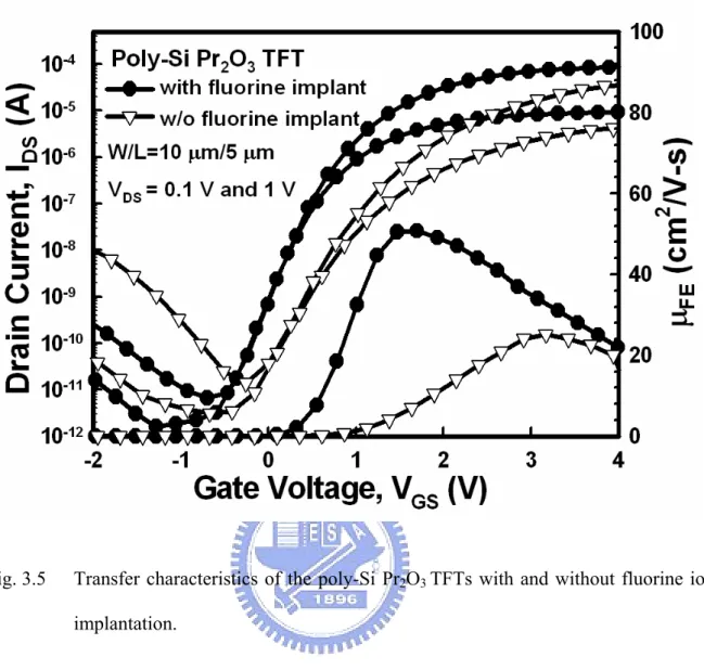
Fig. 3.5 Transfer characteristics of the poly-Si Pr2O3 TFTs with and without fluorine ion
implantation…..……….………52 Fig. 3.6 Plot of ln[IDS/(VGS−VFB)] versus 1/(VGS−VFB)2 at VDS= 0.1 V and high gate
voltage for the fluorine-implanted and control poly-Si Pr2O3
TFTs..………..………..53 Fig. 3.7 Output characteristics of the fluorine-implanted and control poly-Si Pr2O3
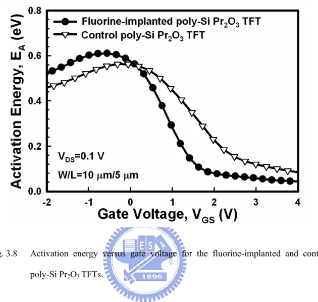
TFTs………..………54 Fig. 3.8 Activation energy versus gate voltage for the fluorine-implanted and control
poly-Si Pr2O3 TFTs………...……….………56
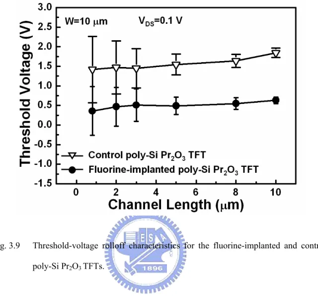
Fig. 3.9 Threshold-voltage rolloff characteristics for the fluorine-implanted and control poly-Si Pr2O3 TFTs……….……..……….57
Fig. 3.10 Threshold-voltage shift over hot-carrier stress time for the fluorine-implanted and control poly-Si Pr2O3 TFTs………..……….…….58
Fig. 3.11 On-current variation over hot-carrier stress time for the fluorine-implanted and control poly-Si Pr2O3 TFTs……….………...59
Fig. 3.12 Cross-sectional TEM image of the proposed Pr2O3 gate dielectric TFTs on CF4
plasma-treated poly-Si film………….………..………….…………..….60 Fig. 3.13 Typical C-V characteristic of the Pr2O3 gate-dielectric MOS capacitor. The inset
figure shows the hysteresis characteristic of the Pr2O3 gate dielectric. …………61
Fig. 3.14 Transfer characteristics of the poly-Si Pr2O3 TFTs with various rf powers of CF4
plasma treatments at VDS = 0.1 V. ………..……….……….62
plasma treatments at VDS = 1 V. ……….………..63
Fig. 3.16 SIMS depth profiles of the fluorine and praseodymium atoms for the poly-Si films with various rf powers of CF4 plasma treatments………65
Fig. 3.17 Plot of ln[IDS/(VGS−VFB)] versus 1/(VGS−VFB)2 under strong inversion at VDS =
0.1 V for the poly-Si Pr2O3 TFTs with various rf powers of CF4 plasma
treatments……..………….……….……….………….…………66 Fig. 3.18 AFM images of the poly-Si films with various rf powers of 0-W, 10-W, and 20-W
CF4 plasma treatments……….………..………68
Fig. 3.19 Activation energy (EA) of the poly-Si Pr2O3 TFTs with various rf powers of CF4
plasma treatments……….……….……69 Fig. 3.20 Threshold-voltage rolloff characteristics of the poly-Si Pr2O3 TFTs with 0-W and
10-W CF4 plasma treatments……….70
Fig. 3.21 Threshold-voltage shift versus hot-carrier stress time for the poly-Si Pr2O3 TFTs
with various rf powers of CF4 plasma treatments……….………71
Fig. 3.22 On-current variation versus hot-carrier stress time for the poly-Si Pr2O3 TFTs
with various rf powers of CF4 plasma treatments……….72
Chapter 4
Fig. 4.1 Schematic diagram of the fabrication processes of the poly-Si TFTs with Argon ion implantation………..………...84 Fig. 4.2 SEM images of the secco-etched poly-Si films with and without Argon ion
implantation after SPC process……….85 Fig. 4.3 XRD patterns of the Argon-implanted and control poly-Si films after SPC
process………...86 Fig. 4.4 The SIMS depth profiles of oxygen and silicon for the Argon-implanted and
control α-Si samples……….………….87 Fig. 4.5 Typical transfer characteristics of the Argon-implanted and control poly-Si TFTs
at VDS = 0.5 V and 5 V…………..……….88
Fig. 4.6 Plot of ln[(IDS/VGS−VFB)] versus 1/( VGS−VFB)2 and the extracted grain-boundary
trap-state densities for the Argon-implanted and control poly-Si TFTs………..….90 Fig. 4.7 Activation energy (EA) of the Argon-implanted and control poly-Si
TFTs………..……….91 Fig. 4.8 Threshold-voltage rolloff of the Argon-implanted and control poly-Si TFTs at VDS
= 0.5 V………..….92 Fig. 4.9 Variation of threshold voltage as a function of stress time for the Argon-implanted
and control poly-Si TFTs………..………….93
Chapter 5
Fig. 5.1 Schematic diagram of the fabrication processes of the poly-Si TFTs with floating-channel structure………..………….……….104 Fig. 5.2 Cross-sectional TEM image of the FC poly-Si TFTs………..…………105 Fig. 5.3 SEM images of the secco-etched poly-Si films with and without floating-channel structure after SPC process……….………….106 Fig. 5.4 Typical transfer characteristics and the extracted field-effect mobility for the FC
and CN poly-Si TFTs with a dimension of W/L = 1 µm/10 µm……..….…..….107 Fig. 5.5 Plot of ln[(IDS/(VGS−VFB)] versus 1/(VGS−VFB)2 and the extracted trap-state
density (Ntrap) for the FC and CN poly-Si TFTs. IDS was measured at VDS = 0.5
V…….……….109 Fig. 5.6 Output characteristics of the FC and CN poly-Si TFTs with a dimension of W/L=
1 µm/10 µm……….110 Fig. 5.7 Threshold-voltage shift versus hot-carrier stress time for the FC and CN poly-Si
TFTs………..………..…….111
Chapter 6
Fig. 6.1 Schematic diagrams of the key fabrication steps of the SPC and MILC poly-Si NW TFTs…..………..123 Fig. 6.2 The cross-sectional TEM image of the poly-Si NW TFT having a couple of NW
channels………...…….…………..………124 Fig. 6.3 Typical transfer characteristics of the SPC poly-Si NW TFTs with and without 1-hr
NH3 plasma treatment……..….…….……….125
Fig. 6.4 Comparison of the normalized transfer characteristics for the standard planar TFT and the NW TFT.………..………..127 Fig. 6.5 Typical transfer characteristics of the MILC NW TFT and the SPC NW TFT with L
= 1 µm and W = 2×50 nm……….……….128 Fig. 6.6 Plot of ln[IDS/(VGS−VFB) versus 1/(VGS−VFB)2 curves at VDS = 0.5 V and the
extracted effective trap-state density………..………130 Fig. 6.7 Threshold-voltage rolloff of the MILC NW TFT and the SPC NW TFT with
channel length (L) varying from 5 µm to 0.8 µm, the channel width (W) is kept at 2×50 nm….……….……….……….………..131
Chapter 1
Introduction
1.1
Overview of Polycrystalline Silicon Thin-Film Transistors
Over the past two decades, polycrystalline silicon Thin-film transistors (poly-Si TFTs) have been widely used in many industrial applications, such as high-density static random access memories (SRAMs) [1.1], electrical erasable programming read only memories (EEPROMs) [1.2], linear image sensors [1.3], thermal printer heads [1.4], photo-detector amplifier [1.5], scanner [1.6], and active-matrix liquid-crystal displays (AMLCDs) [1.7]-[1.9]. In particular, the application of AMLCDs is the major driving force to promote and advance the developments of poly-Si TFT technology.
AMLCD is one of the most promising candidates for realizing large-area flat-panel displays. The application of n-channel amorphous silicon (α-Si) TFTs is constrained in the aspect of pixel switching elements. Hence, it is difficult to integrate pixel switching elements and peripheral driving circuits on single glass substrate for system-on-panel (SOP) applications because of the low electron field-effect mobility (typically below 1 cm2/Vs). Moreover, the electrical properties of p-channel α-Si TFTs are worse than those of n-channel α-Si TFTs, making α-Si TFT technology not practical for CMOS circuits. As a result, poly-Si TFT technology has been steadily growing and become a promising solution for realizing high-performance AMLCD applications due to the advantages of high field-effect mobility, low photocurrents, high driving currents, high CMOS capability, and SOP applications [1.10], [1.11].
reliability. Three major crystallization techniques have been proposed to achieve low-temperature poly-Si TFTs, described as follows.
1.1.1 Traditional Solid-Phase Crystallization (SPC)
Solid-phase crystallization (SPC) technique is usually performed at 600 οC [1.12]-[1.15]. The SPC process is composed of grain nucleation and grain growth. For the traditional SPC of α-Si with homogenous grain nucleation at the α-Si/underlyling SiO2 interface, the
activation energy of the grain growth (3.2 eV) is less than that of the grain nucleation (3.9 eV). Therefore, the amount of the nucleation relative to the grain growth decreases with decreasing temperature. Moreover, such crystallized poly-Si films have a high density of grain-boundary defects and intra-grain defects, which degrade the electrical properties of poly-Si TFTs. An improved SPC technique has been proposed to enlarge the grain size of poly-Si by decreasing the grain nucleation rate even if SPC process is a time-consuming (several hours) process for phase transformation from amorphous into polycrystalline.
1.1.2 Metal-Induced Lateral Crystallization (MILC)
Metal-induced crystallization (MIC) technique with crystallization temperature lower than 600 οC has been studied in the past using trace metals such as Ni, Ge, Al, Au, and Pb [1.16]-[1.20]. However, the grain size of poly-Si is small compared to the feature size of transistor, and an undesirable metal contamination may be introduced at the channel region, degrading the electrical properties of poly-Si TFTs. In addition, poly-Si film with large grain size can be formed by the crystallization of α-Si through metal-induced lateral crystallization (MILC) technique [1.21]-[1-23]. This MILC technique is simple, less contamination, and can be adopted in three-dimensional (3-D) CMOS integrated circuits. The grain size of resulting poly-Si film is significantly enhanced and much larger than the device dimension.
1.1.3 Excimer-Laser Crystallization (ELC)
Excimer-laser crystallization (ELC) of α-Si film on glass substrate gives a good-quality poly-Si with low defect density and no intra-grain defect. Hence, this technique is thought to
be the most preferable crystallization method for the fabrication of poly-Si TFTs [1.24]-[1.28]. While ELC technique is the most commonly used method to manufacture poly-Si TFTs for display applications, there are many ongoing issues, including high manufacturing cost, uniformity concerns over large areas, narrow process window, high process complexity, rough poly-Si/gate oxide interface, and stability of electric performances, need to be resolved to attain a mature ELC poly-Si TFT technology.
Among these three major crystallization techniques, the most widely used method for poly-Si preparation is the SPC technique. Traditional SPC poly-Si TFT has many advantages over ELC poly-Si TFT, such as simplicity, low-cost batch process, high uniformity, and large area capability. Although the maximum processing temperature of SPC poly-Si TFT is limited by the crystallization temperature of around 600 οC, the processing temperature is still considered to be acceptable.
Poly-Si material consists of silicon crystallites (grains). Between them, there are regions with high density of impurities, called grain boundaries. Grain-boundary defects and intra-grain defects existing in the poly-Si film result in a large amount of trap states. The detrimental effect of grain boundaries on the electrical performances of poly-Si TFT has been investigated and been well recognized [1.29], [1.30]. At the turn-on state, the trap states can trap carriers to form potential barriers, and thus affect the on-state carrier transport [1.31]. At the turn-off state, the trap states in the depletion region of drain side result in large off-state leakage currents. The generation of leakage currents can be attributed to a thermionic emission at a low electric field and a field-enhanced emission (i.e. F-P emission or trap-assisted band-to-band tunneling) at a high electric filed [1.32]. The presence of a high density of trap states at the grain boundaries are thought to be related to the Si dangling bonds and Si strain bonds, resulting in severe degradations on the electrical properties of poly-Si TFTs, such as high threshold voltage, low field-effect mobility, large subthreshold swing, and high leakage currents. The grain-boundary effects can be reduced mainly by two
techniques: (1) by passivating the Si dangling bonds at the grain boundaries with plasma treatments and thus reducing the density of the grain-boundary defects [1.33], [1.34]; (2) by enlarging the grain size of poly-Si and thus reducing the number of grain boundaries present within the active channel of poly-Si TFT.
In addition, the device performances could also be improved by adopting novel device structures, including multiple channel structures [1.35], offset source/drain [1.36], [1.37], lightly doped drain (LDD) [1.38], gate-overlapped LDD (GO-LDD) [1.39]-[1.41], field-induced drain (FID) [1.42], and vertical channel [1.43]. This novel device structures focus on decreasing the electric field near the drain junction, and thus suppresses the off-state leakage currents of poly-Si TFTs.
1.2
Motivation
To realize SOP purposes, integrating pixel switching and peripheral driving ICs on single glass substrate are required [1.44]. However, it is a challenge to develop high-performance poly-Si TFTs for both pixel TFTs and display driving circuits [1.45]. To drive the liquid crystal, pixel TFTs operate at high voltages with low gate-leakage currents. In contrast, TFTs with low operation voltages, low subthreshold swing, high driving capability, and low gate-leakage currents are required for approaching high-speed display driving circuits. However, traditional SPC poly-Si TFTs with continued scaling SiO2 gate
dielectric can increase the driving currents of poly-Si TFTs. But, a thinner SiO2 gate
dielectric cannot still satisfy these demands due to the high gate-leakage currents and poor electrical reliability [1.46]. With the same physical gate-dielectric thickness, introducing high dielectric constant (high-κ) material to replace SiO2 as the gate dielectric can increase
the gate capacitance density and then induce much more mobile carrier density in the channel region. Therefore, several high-κ gate dielectrics including ONO gate stack, Al2O3,
HfO2, and LaAlO3, have been proposed as replacement for SiO2 gate dielectric to improve
the electrical performances of poly-Si TFTs due to better gate controllability [1.47]-[1.50]. Unfortunately, the implementation of ONO gate stack and Al2O3 could not effectively
improve the device performances due to their lower dielectric constant. On the other hand, these polycrystalline high-κ materials might not be sufficiently stable under post-annealing process. Recent studies reported that thermally robust praseodymium oxide (Pr2O3) appeared
as a promising high-κ gate dielectric in MOSFET owing to its outstanding dielectric properties, including high dielectric constant value of about 31, ultra-low gate-leakage currents, and superior reliability characteristics [1.51], [1.52]. In Chapter 2, poly-Si TFTs with high-κ Pr2O3 gate dielectric are demonstrated and investigated.
Nevertheless, such high gate capacitance density contributes to a high electric field at the gate-to-drain overlap area, resulting in more undesirable gate-induced drain leakage (GIDL) currents [1.53]. To address this GIDL current issue, a hydrogen-based plasma treatment technique is mostly adopted for reducing the trap states because hydrogen atoms can easily passivate the trap states at the poly-Si /gate dielectric interface and in the poly-Si grain boundaries [1.54]-[1.57]. However, the hydrogenated poly-Si TFTs suffer from a serious instability issue due to the easily broken of weak Si-H bonds under electrical stress [1.58]. The other promising strategy, fluorine passivation technique, has been utilized to improve the device performance by eliminating the trap states at the grain boundaries. In addition, strong Si-F bonds, more stable than Si-H bonds, can significantly improve the device reliability under long-term electrical stress [1.59], [1.60]. In Chapter 3 and 4, both fluorine ion implantation and low-temperature CF4 plasma treatment on poly-Si films are
developed to effectively introduce fluorine atoms into the poly-Si film. Incorporating these two fluorine-passivated techniques into poly-Si TFTs with Pr2O3 gate dielectric are proposed
and studied.
of poly-Si TFTs [1.61]-[1.63]. For the traditional SPC process, an interface-nucleation scehme with too many nucleation sites at the α-Si/underlying SiO2 interface results in a
small grain size and a large number of grain-boundary trap states [1.64]-[1.67]. Thus, many studies have been proposed to improve the microstructure of poly-Si film by introducing oxygen rich region at the α-Si/underlying SiO2 interface [1.68], [1.69]. The interface
nucleation is effectively suppressed, and then the nucleation process with fewer nucleation sites initiating on the top free surface of α-Si film results in large grain size of poly-Si film. In Chapter 4 and 5, two kinds of grain-size enhancement techniques associating with the surface-nucleation scheme, including deep Argon ion implantation into the α-Si/underlying SiO2 interface and novel floating-channel structure are proposed. Poly-Si TFTs with deep
Argon ion implantation and floating-channel structure are demonstrated and investigated. In addition, a lot of efforts have been put forth to improve the gate controllability and device performance by changing device structure of poly-Si TFTs with complicated steps, such as gate-overlapped lightly doped drain (GO-LDD) TFT [1.70], double-gate TFT [1.71], and gate-all-around TFT [1.72]. Besides, poly-Si TFTs with nano-scale feature sizes have also been proposed to reduce the influences of grain-boundary defects [1.73]-[1.77]. In these studies, the electrical performances of poly-Si TFTs could be remarkably improved by decreasing the channel dimensions to be comparable to, or still smaller than, the grain size. However, poly-Si TFTs with narrow-width channels are directly defined by using costly electron-beam lithography (EBL) technology [1.73]-[1.75], which could not be practicable in flat-panel displays (FPDs). On the other hand, for the poly-Si TFTs with nanowire (NW) channels and multiple-gate configuration reported in [1.76], [1.77], the gate-induced drain leakage (GIDL) currents resulted from large gate-to-drain overlapping area is high and must be addressed by additional processes. In Chapter 6, we demonstrate a simple sidewall spacer technique to fabricate poly-Si TFTs with self-aligned formation of twin NW channels without any expensive photolithography process. Poly-Si TFTs with NW channels
crystallized by traditional SPC technique and advanced MILC technique are proposed and investigated.
1.3
Thesis Organization
This thesis is organized as follows,
In Chapter 1, the overview of poly-Si TFTs and the motivations of this thesis are described.
In Chapter 2, TiN metal gate and high-κ Pr2O3 gate dielectric are integrated into the
SPC poly-Si TFTs. The integrity of the high-κ Pr2O3 gate dielectric is explored. The
electrical characteristics and the short-channel effects of the poly-Si TFTs with Pr2O3 gate
dielectric are studied.
In Chapter 3, two kinds of fluorine passivation effects using fluorine ion implantation and low-temperature CF4 plasma treatments are applied to the poly-Si TFTs with Pr2O3 gate
dielectric are investigated. Effects of fluorine ion implantation and various rf powers of CF4
plasma treatments on the poly-Si films are explored. The electrical characteristics and reliability of the fluorine-passivated poly-Si TFTs with Pr2O3 gate dielectric are investigated.
In Chapter 4, deep Argon ion implantation with projection range beyond on the a-Si/underlying SiO2 interface is proposed to investigate the microstructure of
postcrystallized poly-Si film. The electrical characteristics and reliability of SPC poly-Si TFTs with Argon ion implantation are demonstrated and studied.
In Chapter 5, poly-Si TFTs with floating-channel structure crystallized by solid-phase crystallization process are proposed and fabricated. The grain size and trap-state density of poly-Si film with floating-channel structure are analyzed; moreover, the electrical characteristics and reliability of SPC poly-Si TFTs with floating-channel structure are explored and studied.
In Chapter 6, a simple sidewall spacer technique is proposed for the formation of nano-scale channel width (nanowire, NW) without advanced photolithography system. The crystallization of poly-Si NW channels is formed by the SPC and MILC techniques. Effects of gate controllability on the proposed SPC NW TFTs and standard planar TFTs are explored. Besides, the electrical properties of the MILC NW TFTs and the SPC NW TFTs are demonstrated and investigated.
In Chapter 7, conclusions as well as some recommendations for further research are given.
Chapter 2
High-Performance Polycrystalline Silicon Thin-Film
Transistors with High-
κ Pr
2O
3Gate Dielectric
2.1 Introduction
Polycrystalline silicon thin-film transistors (poly-Si TFTs) have attracted much attention in active-matrix liquid crystal displays (AMLCDs) for the sake of realizing the integration of peripheral driving circuits and pixel switching elements on single glass substrate to accomplish system-on-panel (SOP) purposes [2.1]-[2.3]. High-performance poly-Si TFTs with low operation voltages, low subthreshold swing, high driving capability, and low gate-leakage currents are required for approaching high-speed display driving circuits. However, traditional solid-phase crystallized (SPC) poly-Si TFTs with continued scaling SiO2 gate dielectric can not satisfy these demands [2.4]. In order to address these
issues, integrating metal gate on high dielectric constant (high-κ) gate dielectric with poly-Si TFTs has received lots of attention for maintaining a higher gate capacitance density, a lower gate-leakage current, and a much more induced carrier density [2.5]-[2.11]. Besides, the trap states at poly-Si grain boundaries also could be quickly filled up to improve the subthreshold swing even without additional hydrogenation treatments [2.7]. Therefore, several high-κ gate dielectrics including ONO gate stack, Al2O3, HfO2, and LaAlO3 have been investigated as
replacement for SiO2 gate dielectric to improve the electrical performances owing to better
gate controllability [2.8]-[2.11]. Unfortunately, the implementation of ONO gate stack and Al2O3 could not effectively improve the device performances due to their lower dielectric
stable under post-annealing process. Recent studies reported that thermally robust praseodymium oxide (Pr2O3) appeared as a promising high-κ gate dielectric in MOSFET
owing to its outstanding dielectric properties, including high dielectric constant (~31), ultra-low gate-leakage currents, and superior reliability characteristics [2.12], [2.13].
In this chapter, integrating TiN metal gate on high-κ Pr2O3 gate dielectric with SPC
poly-Si TFTs is successfully demonstrated for the first time. The proposed poly-Si Pr2O3
TFTs show outstanding electrical characteristics as compared to poly-Si tetraethoxysilane (TEOS) TFTs; hence, poly-Si Pr2O3 TFTs can satisfy the needs of peripheral driving circuit
applications with low operation voltages.
2.2 Experiments
The cross section of the proposed poly-Si TFTs with TiN metal gate and Pr2O3 gate
dielectric is depicted in Fig. 2.1. The detail device fabrication is summarized below. First, a 100-nm amorphous silicon (α-Si) was deposited on 500-nm thermally oxidized Si wafers using low-pressure chemical vapor deposition (LPCVD) system at 550 οC [Fig. 2.1(a)]. Subsequently, the SPC annealing process at 600 οCfor 24 h in N2 ambient was used to
crystallize the α-Si film. After the active regions were defined [Fig. 2.1(b)], a 33.6-nm Pr2O3
gate dielectric was deposited by using electron-gun evaporation system, and then annealed at 600 οCfor 30 min in O2 ambient to improve thin-film quality. After the deposition of a
200-nm TiN film, a Cl2 based plasma etching process capable of stopping on the Pr2O3 layer
was used to pattern the gate electrode [Fig. 2.1(c)]. A self-aligned phosphorous ion implantation was performed, followed by the dopant activation at 600 οC for 30 min in N2
ambient [Fig. 2.1(d)]. After a 300-nm passivation SiO2 was deposited by plasma-enhanced
CVD (PECVD), the definition of contact holes were achieved with the selective wet etching of passivation SiO2 and Pr2O3 by buffered oxide etch (BOE) and H2SO4/H2O2 solutions
[2.14], respectively [Fig. 2.1(e)]. Finally, the fabricated poly-Si Pr2O3 TFTs were sintered at
400 οC after the aluminum pad formation [Fig. 2.1(f)]. Moreover, the poly-Si TFTs with a 35-nm TEOS gate dielectric deposited by PECVD were also fabricated with the same process flow for comparison. Note that all the poly-Si TFTs had no hydrogenation treatment in this work.
2.3 Results and Discussion
2.3.1 Pr
2O
3Gate Dielectric Integrity
The cross-sectional transmission electron microscopy (XTEM) image of the proposed poly-Si TFTs is shown in Fig. 2.2, which indicates a physical thickness of Pr2O3 gate
dielectric around 33.6 nm with a 1.5-nm interfacial SiO2-like layer. An accumulation
capacitance of 532 nF/cm2 is achieved for Pr2O3 gate dielectric from capacitance-voltage
(C-V) measurement as shown in Fig. 2.3. Therefore, the equivalent-oxide thickness (EOT) was extracted to be 6.5 nm. The effective dielectric constant (κPr2O3) of Pr2O3 gate dielectric
was extracted by using a Pr2O3/interfacial-SiO2 series capacitor model, expressed as Eq. (2.1)
[2.15].
2 2 2 3
2 3
interficial-SiO interfacial-SiO Pr O Pr O
EOT =T
+ (k
/k
)
×
T
………..Eq. (2.1)where κPr2O3 and κinterfacial-SiO2 are the dielectric constants for Pr2O3 and interfacial-SiO2 films,
respectively, and TPr2O3 and Tinterfacial-SiO2 are the thicknesses of these films. Based on the
relation in Eq. (2.1), the κPr2O3 was evaluated to be 26.2 by assuming the κinterfacial-SiO2 to be
3.9. Moreover, no C-V hysteresis characteristic on Pr2O3 gate dielectric occurs after
repeating ±4 V forward and reverse stresses for 100 times.
Fig. 2.4 shows the gate current density versus electric field (J-E) characteristic of the Pr2O3 gate dielectric film. The J-E characteristic of the Pr2O3 gate dielectric was measured by
gate dielectric. Obviously, the breakdown field of the Pr2O3 gate dielectric is around 6.8
MV/cm, which is larger than that of the PECVD TEOS oxide of 5.4 MV/cm. Therefore, such high gate capacitance density, low charge-trapping phenomenon, and high dielectric breakdown field suggest that the Pr2O3 film is a promising high-κ gate-dielectric candidate
for replacing conventional SiO2 film in the poly-Si TFTs.
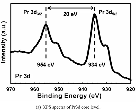
The chemical composition of the Pr2O3 gate dielectric was determined by x-ray
photoelectron spectroscopy (XPS) measurement. In this perspective, the XPS analysis was performed on a 33.6-nm Pr2O3 thin film. The XPS spectra of the Pr3d and O1s core level
spectral regions are displayed in Figs. 2.5(a) and 2.5(b), respectively. The Pr3d signals consist of the 3d5/2 and 3d3/2 spin-orbit doublets. The main Pr3d XPS peak is centered at 934
eV, and its spin-orbit component is well separated at 954 eV. The shape, binding-energy values, and spin-orbit splitting associated with present Pr2O3 features are in agreement with
previous reported data and indicate the existence of the Pr2O3 phase [2.16]. The shape of O1s
XPS feature is quite complicated because of the overlap of different contributions. The visible peak at lower binding energy of 530 eV can be regarded as the Pr-O bonding. At higher binding energy of 533 eV, there is a broad signal due to the overlap of different components associated with SiO2 and hydroxides, that are formed on the film surface.
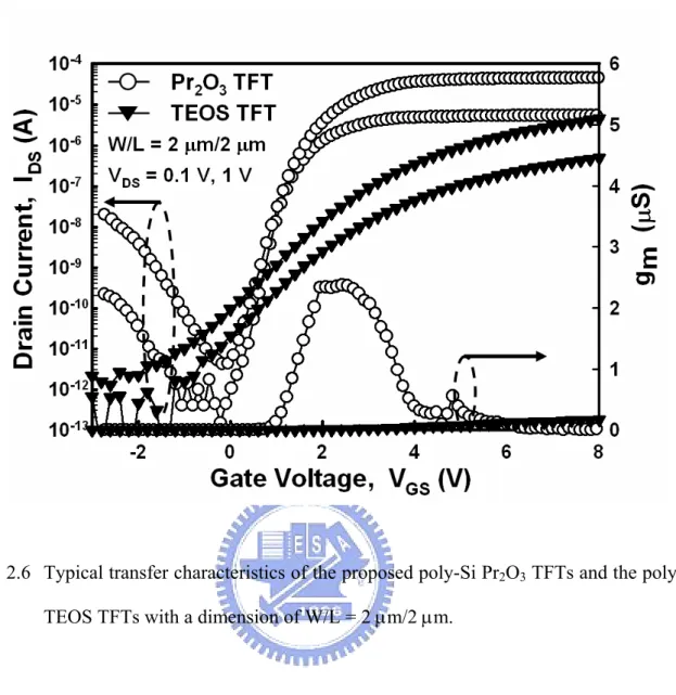
2.3.2 Device Characteristics
Fig. 2.6 shows the typical transfer characteristics (IDS-VGS) and transconductanes for the
proposed poly-Si TFTs with Pr2O3 and TEOS gate dielectric with a dimension of
width/length (W/L) = 2 µm/2 µm. The threshold voltage (VTH) is defined as the gate voltage
required a normalized drain current of IDS = (W/L)×100 nA at VDS = 0.1 V. The ON/OFF
current ratio (ION/IOFF) is defined as that ratio of the maximum on-state current to the
minimum off-state current at VDS = 1 V. The poly-Si Pr2O3 TFT exhibits superior electrical
1.27 V, subthreshold swing (S.S.) improved from 1.08 to 0.22 V/dec., field-effect mobility (µFE) enhanced from 23 to 40 cm2/V-s, and ION/IOFF ratio increased from 3.5×10⁶ to 10.6×10⁶.
However, undesirable gate-induced drain leakage (GIDL) currents of the poly-Si Pr2O3 TFTs
are higher than those of the poly-Si TEOS TFTs, especially under a continuously decreasing gate bias. The inferior GIDL currents may be ascribed to the higher electric field near the drain junction owing to the higher gate capacitance density of the high-κ Pr2O3 gate
dielectric. The GIDL current issue could be solved by using lightly doped drain (LDD) structure [2.17].
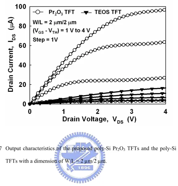
2.3.3 Output Characteristics
Typical output characteristics (IDS-VDS) of the proposed poly-Si Pr2O3 TFTs and poly-Si
TEOS TFTs are illustrated in Fig. 2.7. The device has a drawn channel length (L) and channel width (W) of 2 µm and 2 µm, respectively. As can be seen, the driving current of the poly-Si Pr2O3 TFTs (around 97 µA) is approximately six times larger than that of the poly-Si
TEOS TFTs (around 16 µA) at VDS = 4 V and common gate drive of VGS–VTH = 4 V. This
driving current enhancement results from the high capacitance density induced higher mobility and smaller threshold voltage for the poly-Si Pr2O3 TFTs compared with the poly-Si
TEOS TFTs. Also, These excellent performances of poly-Si TFTs can be approached by SPC technique, without extra plasma treatments [2.6], or other advanced phase crystallization techniques with narrow process window [2.18], [2.19]. Hence, this large driving capability is attractive for high-speed peripheral driving IC’s applications.
2.3.4 Comparison with Other Researches
The measured and extracted device parameters are summarized in Table 2.1, including the other reported data for the SPC poly-Si TFTs with HfO2 [2.10] and LaAlO3 [2.11] gate
with high-κ gate dielectrics. Without narrow channel-width effect [2.20], the calculated field-effect mobility of the poly-Si Pr2O3 TFTs is competed with that of the other reported
poly-Si high-κ TFTs. By using refractory metal TiN [2.5], [2.6], the self-aligned implantation and dopant activation can be integrated intopoly-Si Pr2O3 TFTs after metal gate formation.
The higher gate capacitance density of high-κ Pr2O3 can quickly fill up the trap states at the
grain boundaries in the poly-Si channel. Therefore, the performances of poly-Si Pr2O3 TFTs
can be further improved, including moderate threshold voltage, lower subthreshold swing, and higher ON/OFF current ratio.
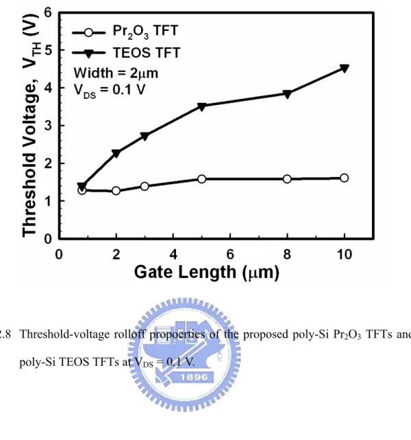
2.3.5 Threshold-Voltage Rolloff
To investigate the short-channel effects of the poly-Si Pr2O3 TFTs and poly-Si TEOS
TFTs, the threshold-voltage rolloff properties are shown in Fig. 2.8. The threshold voltage of the poly-Si TFTs with SiO2 gate dielectric is decreased with continuously scaling down
channel length, dominated by the reduction of grain-boundary trap states. In contrast, the poly-Si TFTs with Pr2O3 gate dielectric exhibit a high gate capacitance density to rapidly fill
up the grain-boundary trap states and holds superior turn-on characteristics, and thus the threshold-voltage rolloff property could be well controlled.
2.4 Summary
High-performance SPC poly-Si TFTs integrated with Pr2O3 gate dielectric and TiN
metal gate have been successfully demonstrated for the first time. This work provides the thinnest EOT of 6.5 nm from the high gate capacitance density of Pr2O3 film. The electrical
characteristics of poly-Si Pr2O3 TFTs can be effectively improved compared to those of
poly-Si TEOS TFTs, including lower threshold voltage, steeper subthreshold swing, higher field-effect mobility, and higher driving current capability, even without additional
hydrogenation treatments or advanced phase crystallization techniques. Therefore, the proposed poly-Si Pr2O3 TFT technology is a promising candidate for future high-speed
(a) Thermal oxidation, and α-Si deposition.
(b) Solid-phase crystallization of α-Si, and patterning of active region.
(d) Self-aligned phosphorus ion implantation, and dopant activation.
(f) Al deposition, patterning of metal pad, and thermal sintering.
Fig. 2.1 Schematic process flows of the poly-Si TFTs with TiN metal gate and Pr2O3 gate
Fig. 2.3 The capacitance-voltage measurement of the Pr2O3 gate dielectric after repeating ±
Fig. 2.4 Gate-current density versus electric field (J-E) characteristic of the poly-Si TFTs with TiN metal gate and Pr2O3 gate dielectric.
(a) XPS spectra of Pr3d core level.
(a) XPS spectra of O1s core level.
Fig. 2.6 Typical transfer characteristics of the proposed poly-Si Pr2O3 TFTs and the poly-Si
Fig. 2.7 Output characteristics of the proposed poly-Si Pr2O3 TFTs and the poly-Si TEOS
Table 2.1 Electrical characteristics comparison for SPC poly-Si TFTs with various gate dielectrics, including Pr2O3 as well as TEOS oxide from this work, HfO2, and
Fig. 2.8 Threshold-voltage rolloff propoerties of the proposed poly-Si Pr2O3 TFTs and the
Chapter 3
Characterizing Fluorine-Ion Implant and CF
4Plasma Treatment Effects on Polycrystalline Silicon
Thin-Film Transistors with Pr
2O
3Gate Dielectric
3.1 Introduction
Polycrystalline silicon thin film transistors (poly-Si TFTs) have received a considerable attention in fields such as large-area electronic applications including linear image sensors and active-matrix liquid crystal displays (AMLCDs) [3.1], [3.2]. The major application of poly-Si TFTs in AMLCDs lies in integrating the peripheral driving circuits and the pixel switching elements on the same glass substrate to realize system-integration-on-panel (SOP) technology [3.3]. The complicated process can be greatly simplified and then the fabrication cost also can be reduced by realizing SOP technology. Because poly-Si TFTs are usually fabricated on inexpensive glass substrate, low-temperature process is required for the realization of commercial flat-panel displays (FPDs). The solid-phase crystallization (SPC) process with maximum process temperature limiting to 600 °C is widely used to recrystallize amorphous silicon film due to its low production cost and good grain-size uniformity [3.4]. However, it is difficult to develop high-performance and high-reliability poly-Si TFTs that are applicable for both pixel switching elements and peripheral driving circuits. Pixel switching elements require TFTs to operate at high voltages as well as low gate-leakage currents to drive the liquid crystals. In contrast, TFTs with good electrical characteristics including low operation voltages, low subthreshold swings, high driving currents, and low gate-leakage currents are necessary for achieving the peripheral driving circuit applications.
However, the electrical properties of the SPC poly-Si TFTs are not good enough to meet the requirements of driving circuits. The SPC poly-Si TFTs with thinner physical thickness of SiO2 gate dielectric can increase the gate capacitance density to enhance the driving
capability, but higher gate-leakage currents could be introduced by the thinner SiO2 gate
dielectric, which would unavoidably degrade the device performances [3.5].
In order to address this issue, incorporating high-κ gate dielectrics into poly-Si TFTs can increase the gate capacitance density and then induce more mobile carriers in the channel region. To reach the same value of gate capacitance density, the physical thickness of high-κ gate dielectrics can be thicker than that of SiO2 gate dielectrics. Therefore, poly-Si
TFTs with high-κ gate dielectrics can improve the gate controllability for enhancing the driving currents and suppressing the gate-leakage currents. Several high-κ materials including ONO gate stack, Al2O3, and Ta2O5, were proposed to replace conventional SiO2 to
serve as the gate dielectrics of poly-Si TFTs [3.6]-[3.8]. However, the performance enhancement of the foregoing poly-Si TFTs is restricted by the lower dielectric constant of ONO gate stack as well as Al2O3 (κ< 9) and the narrow bandgap of Ta2O5. Recently,
praseodymium oxide (Pr2O3) becomes a promising high-κ gate-dielectric candidate in
MOSFET due to its high dielectric constant value of about 31, low gate-leakage currents, good dielectric properties, and superior thermal stability [3.9], [3.10]. Poly-Si TFTs incorporating Pr2O3 as gate dielectric have been proposed in our previous work [3.11],
Chapter 2, which resolved the issues mentioned previously.
However, such high gate capacitance density would contribute to a high electric field at the gate-to-drain overlap area, resulting in rather high field-enhanced emission rates via the grain-boundary trap states. Therefore, poly-Si TFTs with high-κ gate dielectrics would suffer from more undesirable gate-induced drain leakage (GIDL) currents [3.12]. To address this GIDL current issue, various techniques including hydrogen plasma treatments and fluorine ion implantation on poly-Si films have been applied to greatly improve the device
performances by reducing the trap-state densities [3.13]-[3.16]. However, the hydrogenated poly-Si TFTs suffer from a serious instability issue due to the easily broken of weak Si-H bonds under electrical stress [3.14]. Another promising strategy, fluorine ion implantation, has been utilized to improve the device performances by effectively eliminating the trap states at the grain boundaries. In addition, strong Si-F bonds, more stable than Si-H bonds, formed in the poly-Si film and at the poly-Si/gate dielectric interface can significantly improve the device reliability under long-term electrical stress [3.15], [3.16]. However, the fluorine ion implantation method has troublesome problems in large-area electronics and subsequent high-temperature annealing is also required to activate the implanted fluorine ions and cure implant-indcued damages.
In this chapter, two kinds of simple, effective, and process-compatible fluorine-passivation techniques, fluorine ion implantation and low-temperature CF4 plasma
treatments, have been utilized to introduce the fluorine ions into the poly-Si films for eliminating the trap states. CF4 plasma-treated process is more uncomplicated than
fluorine-implanted process because of the lack of fluorine ion implantation and additional annealing step. We have successfully integrated these two kinds of fluorine-passivation techniques into the poly-Si TFTs with Pr2O3 gate dielectric and characterized their electrical
and reliability characteristics.
3.2 Experiments
Fig. 3.1 illustrates the key fabrication steps for the proposed poly-Si Pr2O3 TFTs with
fluorine ion implantation and CF4 plasma treatments. First, we describe the fluorine ion
implantation process as follows. A 50-nm undoped amorphous silicon (α-Si) layer was deposited on a thermally oxidized Si wafer by dissociation of SiH4 gas in a low-pressure
ion implantation was realized with the accelerating energy and dosage at 10 keV and 5×10¹²
cm-2, respectively [Fig. 3.1(b-1)]. The fluorine ions were implanted into the α-Si layer with the projection range locating at the middle of the α-Si film. Subsequently, a solid-phase crystallization (SPC) process was performed at 600 οCfor 24 h in N2 ambient for phase
transformation from amorphous to polycrystalline and activation of fluorine-ion dopants. Individual active regions were patterned and defined [Fig. 3.1(c-1)]. A 40-nm Pr2O3 gate
dielectric was deposited by electron-beam evaporation system, and densified at 600 οC for 30 min in O2 ambient to improve the gate-dielectric quality. Second, we depict the CF4 plasma
treatment technique as follows. A 100-nm α-Si layer was deposited on a thermally oxidized Si wafer [Fig. 3.1(a-2)], and then followed by the realization of SPC process and the definition of individual active region [Fig. 3.1(b-2)]. After RCA clean process, a CF4 plasma
treatment process was applied on the recrystallizaed poly-Si film by plasma-enhanced CVD (PECVD) system at 350 οC [Fig. 3.1(c-2)]. The chamber pressure and flow rate of CF4
reaction gas were 400 mtorr and 80 sccm, respectively. To investigate the effect of CF4
plasma treatments on the poly-Si Pr2O3 TFTs, various radio frequency (rf) powers of 0 W, 10
W, and 20 W, with a constant treating time of 20 s, were used to perform the CF4 plasma
treatments. A 33.6-nm Pr2O3 gate dielectric was deposited by electron-beam evaporation,
followed by a realization of thermal annealing treatment at 600 οC for 30 min in O2 ambient.
Afterwards, the fluorine-implanted and CF4 plasma-treated poly-Si films were performed
with the same following processes. After a 200-nm TiN film was deposited, a Cl2 based dry
etching process capable of stopping on the Pr2O3 layer was used to pattern the gate electrode
[Fig. 3.1(d-1) and 3.1(d-2)]]. A self-aligned phosphorous ion implantation was performed to dope the source/drain regions and then the dopant was activated by the thermal budget of 600 οC for 30 min [Fig. 3.1(e)]. After a 300-nm passivation SiO2 layer was deposited by
PECVD system at 300 οC, the contact holes were opened by a two-step wet etching process. The 300-nm passivation SiO2 layer and the Pr2O3 layer were etched away by a buffered
oxide etch (BOE) solution and a H2SO4/H2O2 mixture solution, respectively [Fig. 3.1(f)].
Since the H2SO4/H2O2 mixture solution has rather high etching selectivity of the Pr2O3 film
to the passivation SiO2 layer, the Pr2O3 film can be completely etched away by an excess of
overetching. Finally, a typical 400-nm Al metallization completed the fabrication process [Fig. 3.1(g)]. For comparison, the control poly-Si Pr2O3 TFTs without the fluorine ion
implantation step and the CF4 plasma treatment, rf power of 0 W, were also prepared with the
same process flow. In order to study the fluorine-passivation effects on the poly-Si Pr2O3
TFTs, no additional hydrogen plasma treatment and thermal sintering process were performed after the Al electrode formation.
3.3 Results and Discussion
3.3.1 Fluorine-Ion Implant Effect on Pr
2O
3TFTs
3.3.1.1 Pr
2O
3Gate Dielectric Integrity
The cross-sectional transmission electron microscopy (XTEM) image of the integrated Pr2O3 gate dielectric on the fluorine-implanted poly-Si TFTs is depicted in Fig. 3.2. From the
XTEM image, the physical thicknesses of the Pr2O3 gate dielectric and the poly-Si channel
are around 40 nm and 48 nm, respectively. The higher resolution XTEM image near the Pr2O3/poly-Si interface displayed in the inset of Fig. 3.2 exhibits an around 1.5-nm SiO2-like
interfacial layer between the Pr2O3 gate dielectric and poly-Si channel. A
metal-oxide-semiconductor (MOS) capacitor with Pr2O3 gate dielectric on single-crystalline
Si wafer was also fabricated to obtain the gate capacitance density of Pr2O3 gate dielectric.
Fig. 3.3 shows typical capacitance-voltage (C-V) characteristics of the MOS capacitor at 1 MHz. The MOS capacitor has the same gate-dielectric thickness as the proposed TFT device has. An accumulation gate capacitance density (Cacc) at applied gate voltage of VG = −4 V is
extracted from the accumulation gate capacitance density is 7.4 nm. The effective dielectric constant of the Pr2O3 gate dielectric was extracted by using a series capacitance of Pr2O3 gate
dielectric and SiO2-like interfacial layer according to the series capacitor model [3.17],
expressed as Eq. (3.1).
2 3
2 3
interfacial layer interfacial layer Pr O Pr O
EOT = T
+(
κ
/
κ
)
×
T
…………..Eq. (3.1)where κPr2O3 and κinterfacial layer are the dielectric constants of Pr2O3 gate dielectric and
SiO2-like interfacial layer, respectively, and TPr2O3 and Tinterfacial layer are the thicknesses of
these films. Here, the TPr2O3 and Tinterfacial layer are assumed to be 40 nm and 1.5 nm,
respectively, and the κinterfacial layer is assumed to be 3.9 to simplify the calculation. Based on
the relation in Eq. (3.1), the effective dielectric constant of the Pr2O3 gate dielectric (κPr2O3)
is extracted to be 26. The inset in Fig. 3.3 shows the hysteresis characteristics of the Pr2O3
gate dielectric upon sweeping from accumulation to inversion (−4 V to 4 V) and then sweeping back (4 V to −4 V). The Pr2O3 gate dielectric demonstrates a negligible hysteresis
characteristic of 7.2 mV. Therefore, such high gate capacitance density, and low charge-trapping phenomenon suggest that the Pr2O3 film is a promising high-κ
gate-dielectric candidate for replacing conventional SiO2 film in the poly-Si TFTs.
3.3.1.2 Evidence of Fluorine Incorporation
Fourier transform infrared spectroscopy (FTIR) and secondary ion mass spectroscopy (SIMS) analyses were utilized to verify the fluorine existing in the poly-Si film. The FTIR spectra of the fluorine-implanted and control poly-Si films after SPC process are shown in Fig. 3.4(a). The main peak of functional group Si-F bonds is clearly observed at around 930 cm-1 in the fluorine-implanted poly-Si film [3.18]. The stronger peak of Si-O bond is derived from the underlying thermal SiO2 substrate. Therefore, Si-F bonds are formed in the poly-Si
fluorine and praseodymium atoms for the fluorine-implanted poly-Si film. It was apparently observed that considerable fluorine ions were detected in the poly-Si film and, in particular, two obvious fluorine peaks were piled up at the Pr2O3 gate dielectric/poly-Si channel and the
poly-Si channel/underlying thermal SiO2 interfaces. Note that the incorporated and piled-up
fluorine ions in the poly-Si film and at the Pr2O3/poly-Si interface would bring about an
effective passivation of deep trap states and interface states, resulting in fewer Si dangling bonds and Si strain bonds.
3.3.1.3 Device Characteristics
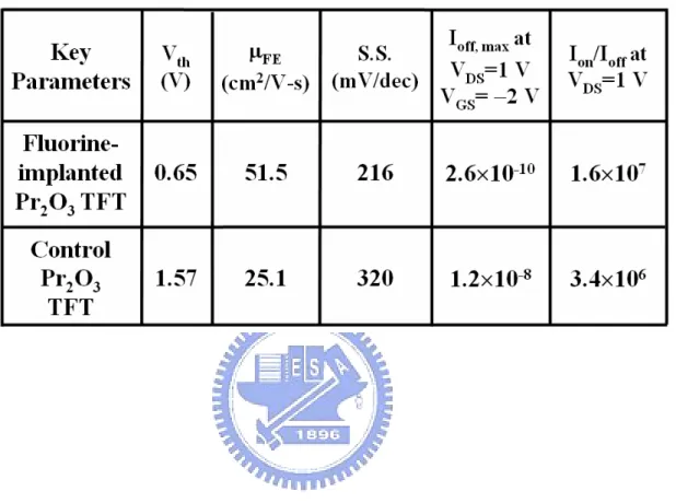
Fig. 3.5 shows the transfer characteristics (IDS-VGS) of the poly-Si Pr2O3 TFTs with and
without fluorine ion implantation. The measurements are performed at two different drain voltages of VDS = 0.1 V and 1 V. The drawn channel width (W) and channel length (L) are
10 µm and 5 µm, respectively. The parameters of the devices, including threshold voltage (Vth), field-effect mobility (µFE), and subthreshold swing (S.S.) are extracted at VDS = 0.1 V,
whereas the maximum off-state leakage currents (Ioff, max) and maximum on-state currents (Ion)
are defined at VDS = 1 V. The on/off current ratio (Ion/Ioff) is defined as the ratio of the
maximum on-state currents to the minimum off-state leakage currents at VDS= 1 V. The
threshold voltage is defined as the gate voltage required to achieve a normalized drain current of IDS = (W/L)×100 nA. The detailed device parameters of the fluorine-implanted and
control poly-Si Pr2O3 TFTs are summarized in Table 3.1.
Accordingly, the electrical performances of the fluorine-implanted poly-Si Pr2O3 TFT
are remarkably improved compared to those of the control poly-Si Pr2O3 TFTs. With the
fluorine ion implantation, the poly-Si Pr2O3 TFTs exhibit significant performance
improvements in terms of drastically decreased threshold voltage from 1.57 to 0.65 V and reduced subthreshold swing from 320 to 216 mV/dec. It is known that the deep trap states, associated with the Si dangling bonds, accompanied with many energy states near the middle