國
立
交
通
大
學
電子工程學系 電子研究所
博 士 論 文
應用於超寬頻通訊系統之互補式金氧半毫米波積體電路
設計與分析
The Design and Analysis of CMOS Millimeter-Wave Integrated Circuits
for Ultra-Wideband Communication Systems
研 究 生:虞繼堯
指導教授:吳重雨 教授
應用於超寬頻通訊系統之互補式金氧半毫米波積體電路
設計與分析
The Design and Analysis of CMOS Millimeter-Wave Integrated Circuits
for Ultra-Wideband Communication System
研 究 生:虞繼堯 Student:Chi-Yao Yu
指導教授:吳重雨 Advisor:Chung-Yu Wu
國 立 交 通 大 學
電子工程學系 電子研究所
博 士 論 文
A DissertationSubmitted to Department of Electronics Engineering and Institute of Electronics
College of Electrical and Computer Engineering National Chiao Tung University
in partial Fulfillment of the Requirements for the Degree of
Doctor of Philosophy in
Electronics Engineering
June 2008
Hsinchu, Taiwan, Republic of China
應用於超寬頻通訊系統之互補式金氧半毫米波
積體電路設計與分析
學生:虞繼堯
指導教授:吳重雨
國立交通大學電子工程系電子研究所
摘要
可預期的,未來利用無線傳輸的資料量與其所需頻寬將與日俱增,因此毫米 波頻段的超寬頻系統在個人通訊上的使用亦將無可避免。針對此應用,本論文提 出了數種互補式金氧半製程關鍵積體電路元件的架構、設計方式與分析,其中包 含了 (1) 直接注入式鎖定除頻器的模組、分析與設計,(2) 應用於降頻的三階諧 波主動式混波器,(3) 直接降頻接收機前置電路的設計與分析,(4)一個適用於毫 米波頻段的多頻段寬頻壓控震盪器。而另一個射頻頻段的低電壓多頻段寬頻壓控 震盪器也在此提出。 首先,本論文將分析適用於毫米波頻段的直接注入式鎖定除頻器,並且將建 立其等效模組,利用此模組將可歸納出數個設計規則用以最佳化除頻器的效能, 如頻率鎖定範圍。為了驗證所提出的等效模組與設計規則,一個不使用可變電容 的直接注入式鎖定除頻器採用了 0.13 微米的互補式金氧半製程來製作。在此除 頻器中,P 型電晶體電流源將用以限制其輸出電壓振幅與增加輸入電晶體的直流 驅動跨壓以加大頻率鎖定範圍。此除頻器的輸入電晶體長寬分別僅為0.12 與 3.6 微米,而所量測到的中心頻率與頻率鎖定範圍分別為70GHz 與 13.6%。在 1V 的 工作電壓下,其功率消耗為4.4mW。其次,本論文提出了一個應用於降頻的三階諧波主動式混波器與其設計考 量。此混波器所需的本地振盪頻率僅為傳統基頻混波器的三分之一。因此,與此 混波器整合的壓控震盪器之頻率操作範圍將可被大幅的增進。再者,由於所提出 之混波器利用本地振盪訊號的三階諧波降頻,而三階諧波的極性特徵與基頻完全 相同,因此此混波器將可基頻混波器一樣輕易的擁有平衡架構。此混波器與一整 合的壓控震盪器採用了 0.13 微米的互補式金氧半製程製作。量測結果顯示整合 壓控震盪器的中心頻率為19.48GHz 而頻率操作範圍可達 13.35%,其相對應的射 頻頻率可由54.54GHz 至 62.34GHz。在此射頻頻率範圍中,混波器的平均增益為 7.8dB,且增益變化不超過 2.2dB。其 1dB 增益下降點約為-10.2dBm,而在 1.2V 的工作電壓下,其與壓控震盪器平均功率消耗分別為6.6 與 0.36mW。 再其次,利用所提出之三階諧波主動式混波器,本論文提出了一個適用於毫 米波頻段超寬頻系統的直接降頻接收機,並且使用 0.13 微米互補式金氧半製程 設計。此接收機包含了一個低雜訊放大器、一對三階諧波主動式混波器、基頻放 大器、輸出級與一個正交壓控震盪器。由於使用三階諧波混波器而降低了所需的 本地震盪頻率,正交壓控震盪器的頻率操作範圍將可被大幅的增進。模擬結果顯 示,當中心頻率為20.35GHz 時,正交壓控震盪器的頻率操作範圍可達 19.87%, 其相對應的射頻頻率已足以涵蓋整個毫米波於美國之開放頻段,57 – 64GHz。 而 在此頻段中,接收機的增益在25 至 29.25dB 間,且其雜訊指數在 11.1 至 13.4dB 間。接收機的 1dB 增益下降點約為-28dBm,而正交壓控震盪器在操作頻段中 1MHz 偏移頻率的平均相位雜訊為-96dBc/Hz。接收機的工作電壓為 1.2V,平均 功率消耗為35.6mW。 最後,本論文提出了兩個不同的多頻段寬頻壓控震盪器。其中之一適用於毫 米波頻段。其使用可變電感調整振盪頻率。使用此可變電感調整振盪頻率,壓控 振盪器將可擁有寬頻且多頻段的特性,且其振盪頻率亦不會因此而有所犧牲。利 用90 奈米互補式金氧半製程設計與製作,量測結果顯示,所提出之壓控振盪器
的振盪頻率可由 52.2 調整至 61.3GHz。相對應的中心頻率與調整範圍則分別為 為 56.75GHz 與 16%。當振盪頻率為 61.3GHz 時,10MHz 偏移頻率的相位雜訊 為-118dBc/Hz,而振幅約為-4.55dBV。在 0.7V 的工作電壓下,其功率消耗為 8.7mW,晶片面積為 0.28×0.36 平方公釐。 另一個所提出的多頻段寬頻壓控震盪器則適用於數 GHz 的射頻頻段與低電 壓操作。除了射頻頻段的應用外,此壓控震盪器亦可做為毫米波外差式接收機的 中頻本地振盪訊號源。其使用了反轉型電晶體可變電容且利用一個大電阻隔絕基 底的寄身效應以增大頻率調整範圍。為了降低壓控震盪器增益以增進相位雜訊效 能,此壓控震盪器亦使用了多頻帶切換技術。以 0.18 微米互補式金氧半製程設 計,模擬結果顯示,當工作電壓與頻率調整電壓均為 0.8V 時,其頻率調整範圍 可由4.4 至 5.9GHz,調整百分比為 29.12%。當振盪頻率為 5.52GHz 時,在 1-MHz 偏移頻率的相位雜訊為-109.65dBc/Hz,功率消耗為 1.2mW。 經由模擬與量測結果證實,本論文所提出的關鍵積體電路元件將可用於高效 能、高整合度、全補式金氧半製程的毫米波頻段超寬頻無線通訊系統中。在未來 將針對其他的毫米波頻段積體電路元件整合而成為一個完整的收發器。
The Design and Analysis of CMOS
Millimeter-Wave Integrated Circuits for
Ultra-Wideband Communication Systems
Student: Chi-Yao Yu
Advisor: Chung-Yu Wu
Department of Electronics Engineering & Institute of Electronics
National Chiao Tung University
ABSTRACT
In this thesis, the design methodologies and implementation techniques of CMOS integrated circuits (ICs) for millimeter-wave (MMW) ultra-wideband (UWB) applications are presented. There are four different kinds of MMW ICs presented in this thesis, including: 1) a direct injection-locked frequency divider; 2) a down-conversion third-order sub-harmonic active mixer; 3) a MMW UWB homodyne receiver front-end; and 4) two multi-band voltage-controlled oscillators (VCOs) with a large frequency tuning range in MMW band and RF band for low-voltage applications.
At first, direct injection-locked frequency dividers operated in the millimeter-wave band are analyzed. An analytically equivalent model of the direct injection-locked frequency dividers is developed and important design guidelines for a large frequency locking range are obtained. A direct injection-locked frequency
divider without varactors is designed and fabricated using 0.13-μm bulk- CMOS process to verify the developed model and design guidelines. The size of the input device is only 3.6μm/0.12μm and the measured frequency locking range is 13.6% at 70GHz with a power consumption of 4.4mW from a supply voltage of 1V.
Secondly, a down-conversion third-order sub-harmonic active mixer is analyzed and fabricated with an on-chip VCO using 0.13-μm CMOS technology. The required LO frequency is one third of that required in a fundamental mixer. Because of the decrease in the LO frequency, the frequency tuning range of the integrated VCO can be extended significantly. Moreover, with the essential differential characteristics of the third harmonic components of LO signals, a balanced structure can be achieved without any extra effort as a fundamental mixer. From the measurement results, it can be observed that the tuning range of the VCO is 13.35% at 19.48 GHz with the corresponding RF frequency range from 54.54 to 62.34 GHz. The average gain of the proposed mixer is 7.8 dB and the variation is smaller than 2.2 dB within the tuning range. The input 1-dB compression point is around –10.2 dBm and the power leakage of the 2LO/LO signal at the RF port is smaller than –35/–42.5 dBm, respectively. The average power consumption of the VCO and the mixer core within the operating frequency range are 6.6 and 0.36 mW, respectively.
Thirdly, a homodyne receiver using third-order sub-harmonic active mixers is analyzed and designed by using 0.13-μm CMOS technology. The receiver consists of a low-noise amplifier (LNA), sub-harmonic active mixers, baseband amplifiers, output buffers, and a qudrature VCO. Due to the reduction in the required LO frequency by using the sub-harmonic mixers, the frequency tuning range of the integrated quadrature VCO can be significantly extended. From ADS and SpectreRF
simulation results, the frequency tuning range of the qudrature VCO is 19.87% at 20.35 GHz and the corresponding RF frequency range is sufficient to cover the entire MMW unlicensed band in the U.S. (i.e. 57 – 64 GHz). The gain of the receiver within the unlicensed band is form 25 to 29.25 dB and the noise figure is from 11.1 to 13.4 dB. The 1-dB compression point occurs around -28 dBm. The phase noise of the quadrature VCO at 1-MHz offset is -96 dBc/Hz. The average power consumption of the receiver is 35.6 mW from a supply voltage of 1.2 V.
Finally, two different multi-band VCOs with wide tuning range are proposed. One of them is operated in the MMW band. It employs a single variable inductor for frequency tuning. By employing the proposed frequency tuning scheme, wide-tuning range as well as multi-band operations are achieved without sacrificing its operating frequency. Fabricated in a 90-nm CMOS process, the VCO is capable of covering frequency range from 52.2 to 61.3 GHz. The tuning percentage is 16% at 56.75 GHz. The measured average phase noise within the tuning range is about -102.4 dBc/Hz at 10-MHz offset. The maximum oscillation voltage amplitude is around -4.55 dBV. The VCO core dissipates 8.7 mW from a 0.7-V supply. Chip size is 0.28 × 0.36 mm2.
The other VCO is operated around 5 GHz which can be chosen as the intermediate frequency in an MMW heterodyne receiver. In this situation, the designed VCO can be used as the LO signal generator in the MMW heterodyne receiver to downconvert the intermediate frequency signals to the baseband. Inversion-mode MOS (I-MOS) varactors are used in the VCO to maintain a wide tuning range in the situation that the supply and tuning voltage is lower than 1V. Moreover, a large resistor is inserted between ground and bulk terminals of each I-MOS varactor to further improve the tuning capability. Through this resistor, the
tuning range is increased by 500 MHz (50%). A bandswitching topology is used to ameliorate the adverse effects of highly sensitive I-MOS varactors. The VCO is designed using 0.18-μm CMOS technology. With a 0.8-V supply, it is shown from simulation results that the VCO has a tuning range of 29.12% from 4.4 to 5.9 GHz when tuned from 0 to 0.8 V. The simulated phase noise is -109.65 dBc/Hz at 1-MHz offset from the 5.52-GHz carrier. The power consumption is 1.2 mW.
It is believed that the proposed IC components can be applied to the design of high-performance high-integration all-CMOS wireless communication systems for MMW UWB applications. Further research on the integration of other transceiver components to form all-CMOS MMW UWB systems will be conducted in the future.
誌謝
轉眼間,在交大已度過了兩千多個日子,回想起當初由通訊所碩士畢 業時的茫然,毅然轉入電子所時陌生而害怕的心情,數不清的挫折與沮 喪,到如今幸運的能完成這本博士論文,讓我深刻的體會到,若想讓人生 更為豐富,勢必要在崎嶇的道路上面對挑戰,無論結果如何,都將是無可 取代的經驗與回憶。 在這段過程當中,首先要感謝我的指導教授吳重雨老師多年來在專業 上的指導與適時的鼓勵。在吳老師數十年來費心辛苦建立的平台之上,讓 電路設計門外漢如我,也能夠循序漸進的完成學業,這更讓我心中常常感 念自己是何其幸運,能在這樣一個完整的環境中接受薰陶。另外也要感謝 和藹可親的師母曾昭玲女士,總是在背後默默的付出關心與支持。我還要 感謝陳巍仁老師在最後一段時間給我許多專業上的幫助,讓我的研究更加 的完整。此外也感謝另外三位師長—吳介琮老師、柯明道老師與郭建男老 師給我的許多指導與建議。 在此我要感謝廖以義、周忠昀、林俐如、范啟威、范振麟、王文傑及 黃鈞正七位學長姊,無論是在專業上或是事務上甚至情緒上,每每當我有 困惑時都能費心的指導我與提攜我。也感謝一起打拼的蘇烜毅同學,總是 與我分憂解勞。感謝徐建昌、左仲先、陳世倫、施育全、傅昶綜、周儒明、 黃冠勳學長、曾偉信、盧台祐、顏承正、張智閔、吳書豪、陳建文、徐新 智、陳勝豪、楊文嘉、黃祖德、蕭淵文、蔡夙勇、翟雲、陳柏宏、許順維 以及所有 307 實驗室的同學,因為你們的相伴,讓我在這段時光中多了許 多美好的回憶。 我要致上最深的感謝給我的祖母與雙親,因為你們長年來給我的照 顧、支持及鼓勵,使我能心無旁騖的完成學業並堅持到最後。也要感謝家族中的其他成員總是能讓我隨時隨地感受到家庭的溫暖。最後,我更要感 謝我的妻子李凱薰小姐,總是任勞任怨的支持我與聆聽我,陪伴我走過所 有的挫折。是你們成就了今日的我,僅以此篇論文獻給你們。 虞 繼 堯 誌於 風城交大 九十七年 初夏
CONTENTS
ABSTRACT (Chinese)
i
ABSTRACT (English)
iv
ACHNOWLEDGEMENT
viii
CONTENTS
x
TABLE CAPTIONS
xiv
FIGURE CAPTIONS
xv
CHAPTER 1
INTRODUCTION
1.1 BACKGROUND 1
1.2 REVIEW ON CMOS IC COMPONENTS 2
1.2.1 Frequency Divider 2 1.2.2 Downconversion Mixer 4
1.2.3 Receiver 6
1.2.4 Voltage-Controlled Oscillator 7
1.3 ORGANIZATION OF THIS THESIS 9
CHAPTER 2
DIRECT INJECTION-LOCKED FREQUENCY
DIVIDER
2.1 ANALYTICAL MODEL 19
2.2 CIRCUIT DESIGN 23
2.2.1 Circuit Structure 23 2.2.2 Input Stage 24 2.2.3 PMOS Current Source 25
2.2.4 Integrated Spiral Inductor and Cross-Coupled Pair 25
2.2.5 To integrate with a differential VCO 27
2.3 PHASE NOISE ANLYSIS 27
2.4 EXPERIMENTAL RESULTS 30
2.5 SUMMARY 33
CHAPTER 3
THIRD-ORDER SUB-HARMONIC MIXER
WITH
AN
ON-CHIP
WIDE-TUNING-RANGE
VCO
3.1 FREQUENCY TUNING RANGE OF COMVENTIONAL CMOS VCO 523.2 OPERATIONAL PRINCIPLE 56
3.3 CIRCUIT DESIGN 58
3.4 EXPERIMENTAL RESULTS 60
3.5 SUMMARY 62
CHAPTER 4
MILLIMETER-WAVE UWB HOMODYNE
RECEIVER
4.1 STRUCTURE 82 4.2 CIRCUIT DESIGN 84 4.2.1 LNA 84 4.2.2 Sub-harmonic mixer 86 4.2.3 Quadrature VCO 884.2.4 Baseband amplifier and output buffer 89
4.2.5 Layout Consideration 89
4.3.1 Quadrature VCO 90
4.3.2 LNA 90
4.3.3 Receiver 91
4.4 SUMMARY 93
CHAPTER 5
MILLIMETER-WAVE AND RF VOLTAGE-
CONTROLLED
OSCILLATORS
5.1 MMW VCO 118 5.1.1 Variable inductor 118 5.1.2 Multi-band operation 120 5.1.3 Circuit design 120 5.2 RF VCO 123 5.2.1 Inversion-mode varactor 123 5.2.2 Multi-band operation 125 5.2.3 Circuit design 1255.3 SIMULATION AND EXPERIMENTAL RESULTS 126
5.3.1 MMW VCO 126
5.3.2 RF VCO 129
5.5 SUMMARY 130
CHAPTER 6 CONCLUSIONS AND FUTURE WORK
6.1 MAIN RESULTS OF THIS THESIS 1526.2 FUTURE WORKS 155
REFERENCES
160TABLE CAPTIONS
Table2.1 Performance Comparison between the Proposed CMOS ILFD
and Other CMOS Frequency Dividers 34
Table3.1 Performance Comparison between the Integrated LO Generators
in this and Other Works 63
Table 3.2 Performance Comparison Between the Mixers in this
and Other Works 64
Table 4.1 Performance Benchmark of 3-stage LNAs 94
Table 4.2 Performance Comparison between the Proposed Receiver
and Other Receivers Operated around 60GHz 95
Table 5.1 Performance Benchmark 131
FIGURE CAPTIONS
Fig. 1.1 2:1 flip-flop-based static frequency divider . 13
Fig 1.2 Conventional LC-based ILFD. 13
Fig 1.3 Direct ILFD. 14
Fig 1.4 Block diagram of the heterodyne receiver. 15
Fig 1.5 Block diagram of the half-IF receiver. 16
Fig 1.6 Block diagram of the homodyne receiver. 17
Fig 1.7 Conventional LC-tank MMW VCO structure. 18
Fig. 2.1 A general block diagram of a differential direct ILFD. 35
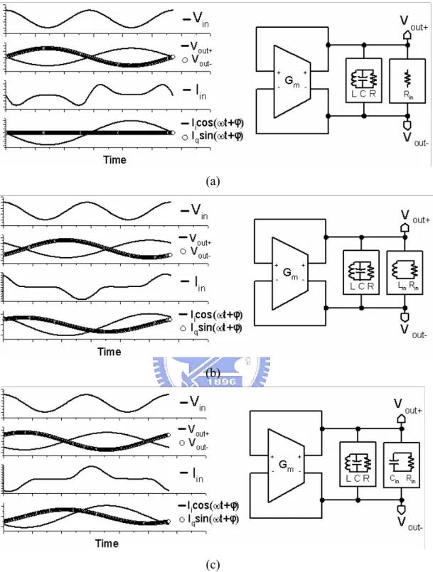
Fig. 2.2 Two waveforms of Vin, Vout±, and Iin as φ is equal to (a) π/2. (b) π/4. 36
Fig. 2.3 The simulated waveforms of Vin, Vout±, Iin, Iicos(ωt+φ), Iqsin(ωt+φ) and the equivalent model as (a) 2ω=2ωo. (b) 2ω>2ωo. (c) 2ω<2ωo. 37
Fig. 2.4 The contour maps of gq,max as (a) vin=0.6V. (b) vin=0.5V. (c) vin=0.4V. (d) vin=0.3V. 39
Fig. 2.5 Circuit structure of the proposed direct ILFD. 40
Fig. 2.6 The simulated frequency locking ranges and gq,max with different values of the inductor. 41
Fig. 2.7 Fig. 2.7 The simulated input sensitivity curves (a) in cases of different input device length. (b) in the cases of different VDD. 42
Fig. 2.8 (a) The block diagram of the direct ILFD. (b) the linear loop for the
phase noise analysis. 43
Fig. 2.9 The simulated curves of Sφn_out/Sφn_in with different (a) ωo (b) Vov
(c) vinat the central frequency 45
Fig. 2.10 The micrographs of ILFDs. 46
Fig. 2.11 The micrographs of ILFDs. 46
Fig. 2.12 (a) The measurement setup for input power measurement. (b) the
measurement setup for divider measurement. 47
Fig. 2.13 (a) The measured output amplitude versus input frequency. (b) the
measured and calculated/simulated locking range and the minimum
output amplitude versus IDC. 48
Fig. 2.14 The locking range as the supply voltages are 0.8V and 1V. 49
Fig. 2.15 The measured locking ranges versus output voltage amplitudes
of both proposed and low-Q ILFDs. 49
Fig. 2.16 The measured input sensitivities of both ILFDs. 50
Fig. 2.17 (a) The measured output phase noise and the phase noise of input
signal from Agilent mm-wave Source Module E8257DS15 [77].
(b) The measured output phase noise and the free-run phase noise. 51
Fig. 3.1 (a) Conventional high-speed VCO (b) equivalent model of the VCO. 65
Fig. 3.3 (a) Equivalent model of a single-finger varactor and (b) equivalent
parallel model when Vtune = 0. 66
Fig. 3.4 Single-turn spiral inductor. 67
Fig. 3.5 Simulation results of: (a) frequency tuning range and (b) Rind. 68
Fig. 3.6 Common-gate amplifier with time-varying transconductance. 69
Fig. 3.7 Simulation results of (a) Gm(t) versus VLO(t) and (b) Gm(t) and
VLO(t) versus t. 70
Fig. 3.8 Simulation results of (a) Gm3, (b) Gm3/IDC, (c) Gm3, and (d) Gm3/Gm0. 72
Fig. 3.9 (a) Circuit schematic and (b) notch filter and its frequency response. 73
Fig. 3.10 Die micrograph. 74
Fig. 3.11 Sub-harmonic mixer measurement setup and environment 75
Fig. 3.12 Frequency tuning range and phase noise. 76
Fig. 3.13 Conversion gain within tuning range. 76
Fig. 3.14 Conversion gain versus IF frequency for different VG. 77
Fig. 3.15 IF power versus RF power. 77
Fig. 3.16 Power leakages of the 2LO and LO signals at RF port. 78
Fig. 3.17 Measured spectrum of IF power and LO-to-IF leakage. 79
Fig. 3.18 Measured spectrum of LO/2LO-to-IF leakages. 80
Fig. 4.1 Architecture of the proposed receiver. 96
Fig. 4.2 Proposed LNA circuit schematic. 97
Fig. 4.3 LNA using conventional cascode structure as the first stage. 97
Fig. 4.4 The simulated NFmin. 98
Fig. 4.5 The simulated S11. 99
Fig. 4.6 Circuit schematic of the proposed third-order sub-harmonic mixer. 100
Fig. 4.7 Circuit schematic of the QVCO. 101
Fig. 4.8 Circuit schematic of the baseband amplifier and output buffer. 102
Fig. 4.9 Circuit layout of the receiver. 103
Fig. 4.10 Interconnections on the (a) RF (b) LO signal path for EM
simulation. 104
Fig. 4.11 Cascode stage of the LNA. 105
Fig. 4.12 Simulation frequency tuning ranges and phase noises of the
integrated QVCO. 106
Fig. 4.13 Monte-Carlo simulation results of (a) phase (b) amplitude errors. 107
Fig. 4.14 Simulation results of S11. 108
Fig. 4.15 Simulation results of LNA voltage gains. 109
Fig. 4.16 Simulation results of LNA noise figures. 110
Fig. 4.18 Simulation results of receiver voltage gains. 112
Fig. 4.19 Simulation baseband frequency responses with different LO
frequencies. 113
Fig. 4.20 Simulation receiver noise figures. 114
Fig. 4.21 Simulation input P1dB. 115
Fig. 4.22 Simulation IIP3. 116
Fig. 4.23 Waveforms of (a) LO (b) baseband output signals. 117
Fig. 5.1 (a) The proposed variable inductor (b) equivalent circuit model. 133
Fig. 5.2 (a) Variable inductor circuit schematic (b) 1:1 transformer layout
view. 134
Fig. 5.3 Simulated Leqand quality factor of VID. 135
Fig. 5.4 Multi-band variable inductor. 135
Fig. 5.5 VCO circuit schematic. 136
Fig. 5.6 VCO small-signal model. 136
Fig. 5.7 (a) Circuit schematic using PMOS current source. (b) simulation results.137
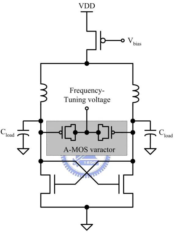
Fig. 5.8 Circuit schematic of the I-MOS varactor. 138
Fig. 5.9 Equivalent model of the I-MOS varactor in (a) depletion
(b) inversion mode. 138
Fig. 5.11 C-V curves of the corresponding A-MOS varactor. 139
Fig. 5.12 VCO schematic. 140
Fig. 5.13 Layout and equivalent model of the spiral inductor. 141
Fig. 5.14 (a) Fabricated VCO circuit schematic. (b) chip micrograph. 142
Fig. 5.15 Measurement setup and environment. 143
Fig. 5.16 Measured and simulated frequency tuning ranges and
oscillating amplitudes. 144
Fig. 5.17 Measured frequency tuning ranges with different supply voltages. 145
Fig. 5.18 Measured frequency tuning ranges of all bands. 146
Fig. 5.19 KVCOof all bands. 147
Fig. 5.20 Measured phase noises and spectrums within the frequency
tuning range. 148
Fig. 5.21 Simulated frequency tuning ranges of the VCO. 149
Fig. 5.22 Simulated frequency tuning range of each band. 150
Fig. 5.23 Simulated phase noise curve. 151
Fig. 6.1 The sub-harmonic receiver with a frequency synthesizer 159
Fig. 6.2 The fundamental receiver and a frequency synthesizer using the proposed MMW VCO in Chapter 5 159
Fig. 6.3 The sub-harmonic receiver and a frequency synthesizer using the proposed direct ILFD in Chapter 2 and MMW VCO in Chapter 5. 159
CHAPTER 1
INTRODUCTION
1.1 BACKGROUND
In the last few years, 7 GHz of contiguous bandwidth have been opened for unlicensed use at millimeter-wave (MMW) frequencies in the U.S. (57-64 GHz) and Japan (59-66 GHz). This allows for various application systems in ultra-wideband (UWB) communication including wireless local area networks (WLANs) with extraordinary capacity, point-to-point ultra-high speed communications (e.g. local multipoint distribution system), short-range high-data-rate Wireless Personal Area Networks (WPANs), local rebroadcasting of high throughput data source (e.g. high definition television within a home), and vehicular radar. With continuing advance of CMOS technologies into nanometer regime, the unit-gain frequency fT of a CMOS
device is beyond 100 GHz. Thus using CMOS technologies to implement integrated circuits operated at MMW frequencies becomes realizable [1]-[3]. With advantages of lower cost and a higher integrated level, CMOS MMW IC components for wireless communication systems have attracted increasing interest and research, recently.
In general, a wireless communication system consists of three functional sub-systems, namely, receiver, transmitter, and frequency synthesizer. The receiver usually includes low-noise amplifiers (LNAs) and down-conversion mixers to perform amplification, downconversion, and demodulation on the received signals. The transmitter includes up-conversion mixers and power amplifiers (PAs) to perform modulation, upconversion, and amplification on the transmitted signals. The frequency synthesizer is used to generate local oscillation (LO) signals in the system.
Its main blocks with the highest operating frequency are the voltage-controlled oscillators (VCOs) and the frequency dividers. The performance of a communication system depends heavily on each of the IC components mentioned above. However, when the operating frequency increases to the MMW band, the substrate loss and low-quality passives in CMOS technology significantly impact the performance of these IC components. Therefore, to maintain high performance in the MMW band, the IC components should be carefully designed and optimized with the help of accurate electromagnetic (EM) simulations to model all passive device/parasitics including routing paths.
In this thesis, the main research focus is on CMOS MMW IC components for UWB communication systems. It includes a frequency divider with a wide frequency locking range, a sub-harmonic mixer suitable for UWB systems, a UWB receiver using the sub-harmonic mixer, and a multi-band VCO with a wide frequency tuning range. Several key IC components will be briefly reviewed in the following subsections.
1.2 REVIEW ON CMOS IC COMPONENTS
1.2.1 FREQUENCY DIVIDER
In general, phase-locked loops (PLLs) are extensively used in CMOS RF front-end systems as frequency synthesizers or clock sources to generate local oscillating signals. In an MMW PLL, the main blocks with the highest operating frequency are typically the VCO and the frequency divider. More specifically, the main design issues of an MMW VCO concern the oscillating frequency tuning range, phase noise, power consumption and output power level [4]-[19]. Most of these
degrade as the input capacitance of the next stage which may be a frequency divider, increases. Therefore, the reduction of the input capacitance of the divider becomes very important as the operating frequency to the MMW band increases. In addition, the wide operating frequency range of the divider is also important for MMW UWB applications. A small operating frequency range will become a bottleneck to extend the operating bandwidth of the MMW PLL. Therefore, the main design challenge facing the MMW divider designers is to reduce input capacitance while maintaining a wide operating frequency range. As in other integrated CMOS RF circuits, power consumption and noise performance are also important in divider design.
Frequency dividers generally can be divided into two groups: flip-flop-based static frequency dividers [20]-[24] and injection-locked frequency dividers (ILFDs) [26]-[38]. The block diagram of a 2:1 flip-flop-based static frequency divider is shown in Fig. 1.1. The internal dividing function is based on a master-slave D-type flip flop by connecting the inverted slave outputs to the master inputs. Such divider usually has a large operating frequency range because it can be operated down to a very low frequency. However, its frequency capability is dominated by the maximum operating frequency of the latches which usually is difficult to reach MMW band in bulk-CMOS technologies. Moreover, the operating frequency becomes even lower if lower power consumption is required.
In comparison with flip-flop-based static frequency dividers, ILFDs generally have lower power consumption and higher frequency capability. However, operating at MMW frequency with a small input capacitance is still difficult by using a conventional LC-based ILFD [26]-[28] as shown in Fig. 1.2. The input stage Min is
large, resulting in a large input capacitance. Moreover, the input signal is significantly degraded by the parasitic capacitor Ctail in Fig. 1.2. By using a peaking inductor
between the drain terminal of Min and the ground, this problem can be reduced [29];
however, this strategy requires a greater chip area. Moreover, the Miller divider proposed in [39] faces the same problems of a large input capacitance and the need for a peaking inductor.
Recently, a direct injection-locked structure [33]-[38] is widely used for MMW frequency division due to its small input capacitance. A typical direct ILFD [34] is shown in Fig. 1.3. At MMW frequency, the input devices Minp and Minn are usually
small to satisfy the specifications of the input capacitance. Such small input devices result in a small injection current and limit the frequency locking range. Therefore, it is important to optimize the frequency locking range of an MMW direct ILFD for UWB applications.
The frequency locking range of a conventional ILFD in Fig. 1.2 has been derived in previous work [25]-[28]. All of them indicate that the phase-limited frequency locking range is inversely proportional to the quality factor (Q factor) of the LC resonator. This result was adopted in the design of direct ILFD [34]-[35] without theoretical verification on the correctness of theory and design. So far, the analytical model and design guidelines for a direct ILFD have not been developed to optimize the frequency locking range.
1.2.2 DOWNCONVERSION MIXER
Downconversion mixer is one of key circuit components in a receiver for frequency translation. The mixers have two distinctly different inputs, namely, the RF
port and the LO port. The RF port senses the signal to be downconverted and the LO port senses the signal generated by the local oscillator, usually a VCO. In general, the main design issues of a downconversion mixer are conversion gain, linearity, noise figure, and port-to-port isolation [40]-[59]. However, when the LO frequency is increased to the MMW unlicensed band, a new problem emerges in bulk-CMOS mixer design for UWB applications. It becomes difficult to integrate the conventional fundamental mixer with a VCO whose frequency tuning range covers the entire MMW unlicensed band, because the input capacitance of the LO port usually is too large. Therefore, it can only be used in narrow band applications [65]-[69].
One solution to increase the frequency tuning range of integrated VCO is to use sub-harmonic mixers to decreases the required LO frequency. Most previous work of sub-harmonic mixers in bulk-CMOS technology [53]-[59] employ second harmonic component of LO signals for frequency conversions. However, for a differential LO signal, the second harmonic component is a single-phase harmonic. By directly using this component, a non-balanced structure can be developed [53]-[54]. Such a non-balanced structure is rarely adopted in the receiver for wireless communication because its LO-to-RF port isolation is poor. Thus the receiver usually prefers differential output signals to reject the common-mode noise. In order to obtain a balanced structure, a differential RF signal or a quadrature LO signal [55]-[59] is required. In comparison with a balanced fundamental mixer, this significantly increases the complexity of circuit design when the mixer is integrated into a receiver.
The third harmonic component of the LO signal has the same polarity as the fundamental component. Therefore, a sub-harmonic mixer employing the third component can retain the balanced structure as a fundamental counterpart with a
single-phase RF signal and a differential LO signal. Moreover, the required LO frequency is lower than those of the mixers using the second harmonic components. So far, the third harmonic component of the LO signal has been successfully used for frequency conversion in a passive downconversion mixer [53]. However, the mixer has a large conversion loss and is still a non-balanced structure which is not suitable for receiver applications in wireless communication.
1.2.3 RECEIVER
Receivers for wireless communication can be divided into two types: heterodyne and homodyne receivers [40]. Both structures have been used in bulk-CMOS receivers operated around the 60-GHz unlicensed band [60]-[69].
A general block diagram of MMW heterodyne receivers is shown in Fig. 1.4. The selection of the intermediate frequency (IF) is an important design issue. For a relatively low IF [61]-[63], the required oscillation frequency of VCORF is high and
the image-reject circuit, which usually degrades the LNA performance, is required to improve the image-reject ratio. For higher IF [60], the required oscillation frequency of VCORF is lower and the image-reject circuit is not required if the image is well out
of band and can be strongly rejected by LNA. The expense of higher IF is that it requires a higher-frequency quadrature LO signal (e.g. VCOIF in Fig. 1.4) or a
high-frequency broad-band phase shifter at IF signal path, which degrades the RF mixer performance. Moreover, the band-pass filter for channel selection for a higher IF usually is more complicated to maintain the selectivity [40].
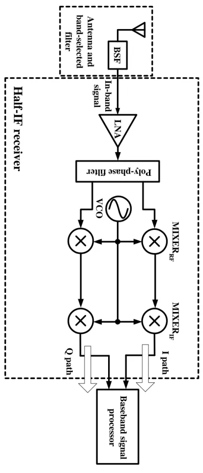
The half-IF receiver shown in Fig. 1.5 [64] is a special case of heterodyne receivers. The main advantage of the half-IF receiver in the MMW band is that the
required oscillation frequency of the VCO is only a half of the frequency of input RF signal. This benefits VCO integration. However, as shown in Fig. 1.5, a high-frequency broad-band poly-phase filter in the RF path and two RF mixers are required to reject the image introduced by the third harmonic of the LO in the RF mixing operation. Moreover, if channel selection needs to be performed in the IF paths, two well match and complex band-pass filters should be inserted into the IF paths. These requirements significantly increase the chip area, integration difficulty and design complexity.
In comparison with heterodyne receivers, the structure of homodyne receivers is more compact as shown in Fig. 1.6. Conventional problems in the homodyne receiver are LO leakage, flicker noise, and DC offset [40]. However, when the operating frequency increases around the 60-GHz unlicensed band, homodyne receivers [65]-[69] suffer from a new problem of the quadrature VCO (QVCO) integration for UWB applications. The required oscillating frequency of the QVCO is too high to maintain its frequency tuning range in bulk-CMOS technologies. Therefore, the main design challenge of the MMW homodyne receiver is to extend the operating frequency range without decreasing the operating frequency while maintaining its relatively simple structure.
1.2.4 VOLTAGE-CONTROLLED OSCILLATOR
In the RF transceiver front-end, LC-tank voltage-controlled oscillators (VCOs) are extensively used in frequency synthesizers to provide local carriers for up and down frequency conversion. In general, the specifications of VCOs such as oscillating frequency, phase noise, output power level, and frequency tuning range significantly affect the performance of the RF transceiver. Therefore, a high-performance
bulk-CMOS VCO is usually required for a highly integrated communication system.
Conventionally, MOS varactors are used in LC-tank VCOs for frequency tuning and can be divided into two types: inversion-mode MOS (I-MOS’s) and accumulation-mode MOS (A-MOS’s) varactors. At several GHz, an I-MOS varactor provides a larger frequency tuning range than an A-MOS varactor [70], especially in the case of a low tuning voltage. By using deep n-well and inserting a large resistor between the I-MOS bulk and ground, the tuning range can be extended further [84]. However, because the electron concentration in the inversion layer cannot change instantaneously, the maximum operation frequency of published VCOs using I-MOS varactor is around 10GHz [85]. Therefore, for MMW applications, such VCO only can be used in a heterodyne receiver to downconvert the IF signal to the baseband (i.e. VCOIF in Fig. 1.4).
LC-tank VCOs operated in the MMW band usually employ A-MOS varactors for frequency tuning [5]-[19]. Fig. 1.7 shows a widely used LC-tank MMW VCO structure. The negative resistance is provided by an NMOS cross-coupled pair to maintain the oscillation. The inductors are implemented by an on-chip center-tapped metal coil. Cload represents the capacitance from the next stages, e.g. buffers,
frequency dividers, or mixers. Obviously, the sizes of the A-MOS varactors dominates the maximum to minimum capacitance ratio of the LC tank and the frequency tuning range for a given cross-coupled pair and Cload. However, when the oscillating
frequency is increased to the MMW band, the sizes of the varactors are strictly limited because of two reasons. Firstly, for the same cross-coupled pair and Cload, the sizes of
varactors should be decreased to decrease the total capacitance of the LC tank for MMW oscillation. Secondly, the quality factor of the LC tank is dominated by the
varactors in the MMW band [17]. Thus small varactors are desired to maintain the quality factor of the LC tank and the oscillation. With these two reasons, the published bulk-CMOS MMW VCOs above 50 GHz [8]-[19] usually suffer form a narrow frequency tuning range which makes the circuits sensitive to process variation and less feasible for UWB applications. To extend the frequency tuning range of the structure shown in Fig. 1.8, the circuit layout should be carefully optimized and some test chips are required for device size trimming [17].
In comparison to the VCO operated at several GHz, the same frequency tuning percentage of an MMW VCO results in a relatively large VCO gain. Therefore, for a wide-tuning-range MMW VCO for UWB applications, multi-band operation is required to degenerate the VCO gain and alleviate phase noise performance when integrated into a broadband frequency synthesizer. However, the conventional capacitor bank for multi-band operation [71]-[74] is no longer applicable at MMW oscillating frequency because its parasitic capacitance is too large. Therefore, a new tuning strategy is required for an MMW VCO to achieve a wide frequency tuning range and multi-band operation without degrading its oscillating frequency.
1.3 ORGANIZATION OF THIS THESIS
It is the aim of this thesis to analysis and design bulk-CMOS ICs for MMW UWB applications. The thesis includes an analytical model and optimization of MMW direct injection-locked frequency divider, the design of third-order sub-harmonic mixer with an on-chip wide-tuning-range VCO, the design of homodyne receiver for MMW UWB applications, and a new frequency tuning strategy for an MMW VCO. Moreover, a wide-tuning-range RF VCO for low-voltage
applications is presented. The VCO can be used as a local signal generator in a MMW heterodyne receiver to downconvert the IF signal to the baseband.
In Chapter 2, an analytical model and design guidelines of a direct ILFD are presented. The proposed model herein reveals that for a direct ILFD, increasing the quality factor of the LC resonator can reduce the power consumption without reducing the frequency locking range. This result differs from the conventional one. Based on the developed model and guidelines, the design methodology for a MMW direct ILFD is given. The phase noise analysis of a direct ILFD is also presented in this chapter. It is shown from simulation results that a direct ILFD has good noise suppression capability in the MMW band. Based on the proposed design methodology, a direct ILFD without a varactor is designed and fabricated by using 0.13-μm bulk-CMOS technology. For comparison purpose, the other direct ILFD using an LC resonator with a lower quality factor is also fabricated on the same chip. Finally, the experimental results are summarized.
In Chapter 3, a new down-conversion third-order active sub-harmonic mixer with on-chip VCO is proposed and designed for MMW UWB applications. The equation of the frequency tuning range of a VCO with A-MOS varators is derived in this chapter. It shows that the frequency tuning range is inversely proportional to the square of the oscillating frequency. Many VCOs are simulated by using HSPICE to verify the theoretical result. The proposed mixer consists of two common-gate amplifiers with differential LO signals from the VCO applied to their gate terminals to modulate the transconductances for frequency conversion. In comparison to a fundamental or second-order sub-harmonic mixer, the tuning range of the integrated VCO can be improved by reducing the oscillating frequency, while retaining the
balanced structure. Moreover, with proper design, the conversion gain of the mixer can be made much larger than that of a passive mixer with only a small increase in the power consumption. With input matching and isolation improving circuit, the proposed mixer with on-chip VCO is fabricated using 0.13-μm bulk-CMOS technology. The experimental results are presented.
In Chapter 4, a homodyne receiver is designed for MMW UWB applications by using the proposed mixer in Chapter 3 and 0.13-μm bulk-CMOS technology. The receiver includes a broadband-matching LNA, active sub-harmonic mixers, a quadrature VCO, IF amplifiers, and output buffers. A single common-source NMOS structure with a source degeneration inductor is used as the first stage of the LNA. From ADS and SpectreRF simulations, the structure has better noise figure and input matching bandwidth in the MMW band in comparison with the conventional cascode structure. Because the required LO frequency is reduced by using the sub-harmonic mixers, the frequency tuning range of the integrated quadrature VCO can be significantly extended. From ADS and SpectreRF simulation results, the tuning range can cover the entire MMW unlicensed band (i.e. 57 – 64 GHz). The IF amplifiers are used to enhance the voltage gain and bandwidth of the receiver. The output buffers are used to drive off-chip 50-Ω load. The ADS post-simulation results of the whole receiver are also given in this chapter. It is shown that the proposed homodyne receiver provides a solution to extend the operating frequency range to the MMW band while maintaining a simple structure.
In Chapter 5, an MMW VCO with a single variable inductor (VID) for frequency tuning is proposed and analyzed. The VID consists of a transformer and a variable resistor. The equivalent inductance of the VID can be varied by adjusting the
resistance of the variable resistor. From the analysis, the lower bound of the frequency tuning range of the VCO with the proposed VID is independent of the oscillating frequency. Therefore, the frequency tuning range is not degraded even when the oscillating frequency is up to MMW band. Moreover, the VID can be modified to achieve multi-band operation by decomposing the variable resistor into several smaller parts. It is shown that the multi-band operation can be achieved without sacrificing the oscillating frequency. The experimental prototype of the VCO is fabricated in 90-nm CMOS technology and the experimental results are presented.
Another RF multi-band VCO for low-voltage applications is also proposed in this chapter. To maintain a fine frequency tuning range in the case of low tuning voltage, I-MOS varactors are used for bandswitching and frequency tuning because of their natural abrupt gradient of the C-V curve (i.e. capacitance relative to tuning voltage curve). A large resistor which connects ground and each I-MOS bulk terminal is used to isolate the I-MOS gate-to-bulk parasitic capacitance and improve the tuning range further. The VCO is designed by using 0.18-μm bulk-CMOS technology and the simulation results are presented.
Q
Q
D
D
Q
Q
D
D
C
C
C
C
INPUT
OUTPUT
D-Latch
D-Latch
Fig 1.1 2:1 flip-flop-based static frequency divider.
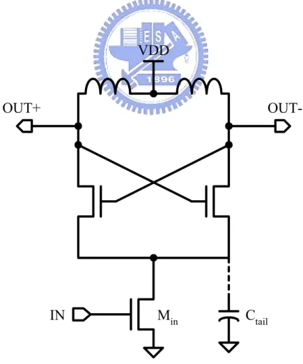
VDD
OUT+
OUT-IN
M
inC
tailOUT+
OUT-IN+
VDD
IN-M
innM
inpIn-ba nd si g n al Qu ad ra tu re VC O IF LN A BSF Ante nna and band-se le cte d filter I pa th Q p a th B a se ba nd si gna l pro ce sso r
Heterodyne receiver
VC O RF MIX E R RF Im ag e-rej ec t circ u it Band-pass filte r for c h annel se lect ion MI X E R IFIn-band signal LNA BSF Antenna and ban d -selected fi lte r I path Q pa th Base ba nd signal p roces sor
Half-IF receiver
VCO Po ly-phase filter MI XE R IF MI X E R RFIn-band
signal
LNA
BSF
Ant
enna
and
b
a
n
d
-select
ed
filter
I pa
th
Q p
a
th
Baseband si
gnal
pr
oce
sso
r
Homodyne receiver
MI
XER
Quadrature
VCO
VDD
V
biasFrequency-Tuning voltage
A-MOS varactor
C
loadC
loadCHAPTER 2
DIRECT INJECTION-LOCKED FREQUENCY
DIVIDER
2.1 ANALYTICAL MODEL
The general block diagram of a differential direct ILFD is shown in Fig. 2.1. The active Gm cell with positive feedback is designed to provide a negative resistance to
compensate for the power loss from the resistive load per oscillating cycle for the stable output oscillating signals. L, C and R represent the equivalent passive loads of the active Gm cell. To reduce the input capacitance for high-frequency operation, the
input stage is implemented by using an NMOS Min only. The input voltage Vin =
vincos(2ωt+φin) is applied to the gate node of Min, where φin is the input phase. For the
sake of convenience it is assumed that φin = 0, as shown in Fig. 2.1. If the input
frequency 2ω falls into the divided-by-2 locking range, then the differential output voltages, Vout±, at the drain and the source nodes of Min are given by ±vocos(ωt+φout),
where φout is the output phase. If φin = 0, then φout can be denoted as φ, which
represents the phase difference between the input and output signals. In this situation,
Min can be regarded as a mixing device and the mixing channel current of Min is
denoted by Iin.
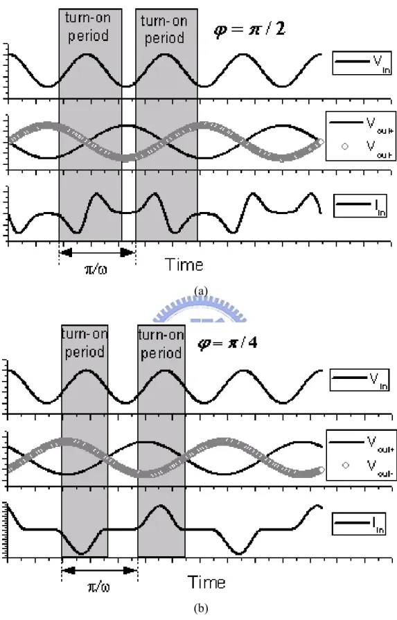
In most cases, the input voltage is a large signal so Min is operated in the on-off
mode. Figs. 2.2(a) and 2.2(b) show the two sample waveforms of Vin, Vout± and Iin as φ
is equal to π/2 and π/4 respectively. As shown in Fig. 2.2, the time interval between the two neighboring turn-on periods of Min is π/ω. Since the frequency of the
differential output voltages at the drain and source nodes of the Min is exactly half of
that of the input voltage, the resulting Iin in the two neighboring turn-on periods
displays the same shapes but opposite polarities as those shown in Figs. 3(a) and 3(b). Therefore, the fundamental frequency of Iin is ω and the fundamental component of Iin
is denoted by Iin,ω.
To develop the desired analytical model, Iin,ω is decomposed into in-phase and
quadrature components:
( ) (
ϕ ω ϕ)
( ) (
ϕ ω ϕ)
ω =I t+ +I t+
Iin, i cos q sin (2.1)
As shown in Figs. 2.2(a) and 2.2(b), the shape of Iin strongly depends on φ. Therefore,
the amplitudes of both components in (2.1) should also be the functions of φ.
In fact, φ is determined by the input frequency 2ω. Figs. 2.3(a) to 2.3(c) plot the HSPICE simulated waveforms of Vin, Vout± and Iin when 2ω is equal to, larger than, or
smaller than 2ωo where ωo is the resonant frequency of the equivalent passive load in
Fig. 2.1. The waveforms of Iicos(ωt+φ) and Iqcos(ωt+φ) calculated from Iin are also
shown in each figure. Fig. 2.3(a) plots the waveforms in the case of 2ω = 2ωo. In this
case, φ equals π/2 and Iq(π/2) = 0, so the phase of Iin,ω is the same as the output
voltage signal. Therefore, the Min can be modeled as a single resistor Rin with the
value of Ii(π/2)/2vo. The equivalent model in this case is also shown in Fig. 2.3(a).
When the input frequency 2ω exceeds 2ωo, as the waveforms plotted in Fig.
2.3(b), φ becomes slightly smaller than π/2 so Iin,ω lags behind the output voltage
signal. Therefore, Iq(φ) is larger than 0 and Min can be modeled as Rin in parallel with
( )
o i in I v R = ϕ 2 (2.2) and Lin =2vo ωIq( )
ϕ ≈2vo ωoIq( )
ϕ . (2.3) The equivalent model in this case is also presented in Fig. 2.3(b). The output frequency ω can be easily calculated as(
)
( )
(
1 2)
( )
4 . || 1 o q o q o o in Cv I LC I Lv L L C ϕ ω ϕ ω ω + ≈ + ≈ = (2.4)Therefore, the maximum available value of ω, ωmax, is determined by the maximum
available value of Iq(φ)/2vo which is denoted by gq,max. ωmax is given by
( )
. 2 2 2 1 ,max max max C g v I C q o o q o ⎟⎟ ≡ + ⎠ ⎞ ⎜⎜ ⎝ ⎛ + ≈ω ϕ ω ω (2.5)The waveforms and the equivalent model of the final case in which the input frequency 2ω is less than 2ωo are shown in Fig. 2.3(c). In this case, φ becomes
slightly larger than π/2 such that Iin,ω leads to the output voltage signal. Therefore, Iq(φ)
is smaller than 0 and Min can be modeled as Rin in parallel with a capacitor Cin, whose
capacitance is given by
Cin =Iq
( )
ϕ 2voω ≈Iq( )
ϕ 2voωo. (2.6) The output frequency ω can be easily calculated as(
)
( )
(
1 2)
|( )
4 |. 1 1 o q o o o q in Cv I Cv I LC C C L ϕ ω ω ϕ ω − ≈ − ≈ + = (2.7)Therefore, the minimum available value of ω, ωmin, is determined by the
minimum available Iq(φ)/2vo which is denoted by gq,min. ωmin can be expressed as
( )
. 2 | | | 2 | 2 1 ,min min min C g v I C q o o q o ⎟⎟ ≡ − ⎠ ⎞ ⎜⎜ ⎝ ⎛ − ≈ω ϕ ω ω (2.8)From (2.5) and (2.8), the input frequency locking range denoted by Δωin can be
calculated as
Δωin =2
(
ωmax −ωmin)
=(
gq,max+|gq,min|)
C. (2.9) Given the symmetric differential structure in Fig. 2.1, for a particular output voltage amplitude vo, gq,max equals -gq,min and (2.9) can be further simplified as. 2 2 q,max o2 q,max in g C ω Lg ω Δ = = (2.10)
According to (2.10), gq,max should be designed as large as possible to maximize
the locking range Δωin for fixed values of L and ωo. However, since all voltage
signals that are applied to Min are large signals, no analytical equation exists for gq,max.
Therefore, HSPICE is adopted to find the values of gq,max in the variously biased cases.
Figs. 2.4(a) to 2.4(d) show contour maps of gq,max for various DC overdrive voltages
Vov of Min and output voltage amplitudes vo with different input voltage amplitudes vin.
In all these cases, gq,max increases with Vov for a fixed vo and decreases as vo
According to the proposed model, shown in Fig. 2.3, and the derived locking range equation, (2.10), for a fixed L, the quality factor Q = R/ωL of the passive load in Fig. 2.3 does not directly influence the locking range. More accurately, the value of
Q only indirectly influences the locking range through a change in Vov or vo which
changes gq,max, as shown in Fig. 2.4. For example, for a given Gm cell, a low Q of the
passive load results in a smaller vo and thus a larger gq,max and the locking range that is
given by (2.10). However, in low and high Q cases, the locking ranges can more fairly be compared with a fixed vo and Vov. In this situation, gq,max is fixed as shown in Fig.
2.4, such that the locking ranges in low and high Q cases are the same for a fixed L and ωo, as determined by (2.10). Since a lower-Q passive load has a lower R, the Gm
cell needs to consume more power in order to compensate for R to maintain the same output voltage amplitude vo at resonance. Therefore, for any required vo, using a
higher-Q passive load can reduce the power requirement without any reduction in the locking range.
From the above analysis, some design guidelines for a direct ILFD can be inferred. Firstly, Vov of the input device should be designed as large as possible to
maximize the gq,max and frequency locking range. Secondly, a trade-off exists between
the output voltage amplitude vo and the frequency locking range. Therefore, vo should
be set at its minimum tolerant value to maximize the frequency locking range. Finally, the Q factor of the passive load should be as large as possible, to reduce the required DC power consumption without reducing the frequency locking range.
2.2 CIRCUIT DESIGN
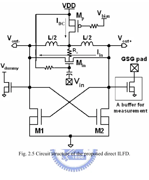
Based on the design guidelines in Section 2.1, the proposed ILFD circuit for high-speed operation is shown in Fig. 2.5. The circuit structure is simple in that it has no varactor but it still provides a large frequency locking range.
In order to reduce the input capacitance, NMOS Min is used as the only input
stage to generate the injected current Iin. Furthermore, instead of a complementary
cross-coupled pair [35], an NMOS cross-coupled pair is used to implement the Gm
cell in Fig. 2. Since the frequency locking range is inversely proportional to the total capacitance value at the output node as in (2.10), the absence of a PMOS cross-coupled pair can significantly increase the frequency locking range. Adding a PMOS current source Mp as shown in Fig. 2.5 provides two advantages over an ILFD
presented in an earlier work [37], increasing the locking range. Firstly, since a trade-off exists between the output voltage amplitude and the frequency locking range, the output voltage amplitude can be set to its minimum value by designing an appropriate DC current of Mp to maximize the locking range. Secondly, the gate
voltage of Min is connected to VDD and the DC voltage at the output node can be set
much lower than the VDD because the DC current is limited by Mp. Therefore, the
Min can be biased in the high overdrive voltage region. Additionally, through the
resistor Rx, the at the substrate node of Min is connected to the common-mode node of
the spiral inductor. The DC voltage at the substrate node can be equal to those at the drain and source nodes such that the threshold voltage of Min can be kept low to
increase overdrive voltage. It should be noted that the threshold voltage of Min is
modulated by the output voltages and affects gq,max. This effect should be considered
in the large signal simulations as the gq,max simulations is the Section 2.1.
Based on the design guidelines proposed in Section 2.1, the locking range of the proposed ILFD can be extended even a small device is used. In this design, the width of the input NMOS Min is designed as 3.6μm, with the minimum length which is
smaller than that in [35]. From the simulation, the input capacitance of Min is less than
10fF, which is an acceptable load for an on-chip 70-GHz VCO.
2.2.3 PMOS Current Source
The DC current of the PMOS current source denoted by IDC directly influences
the output voltage amplitude vo. According to the model in Fig. 4, vo can be estimated
as IDC(R||Rin) [75]. Notably, a trade-off exists between vo and the frequency locking
range. Therefore, IDC should be designed appropriately such that vo just equals the
required value at the edges of the frequency locking range.
2.2.4 Integrated Spiral Inductor and Cross-Coupled Pair
Since the small size of Min constrains the value of gq,max, careful design of an
integrated spiral inductor and cross-coupled pair to achieve a large frequency locking range is important. It can be seen from (2.10), that the frequency locking range is proportional to the inductor value L. Initially the frequency locking range increases with an increase in inductance. However, as L increases over an optimum value, the locking range begins to drop for the following two reasons. Firstly, the output center frequency ωo can be expressed as
(
ov ox next)
o ≈ 1 L 2W1,2C +C W1,2L1,2 3+C
ω (2.11)
where W1,2 (L1,2) is the width (length) of M1 and M2 in Fig. 2.5, Cov is the overlap
capacitance from the next stage. Thus, as L increases, W1,2 must be reduced to
maintain the required ωo. At a fixed DC current, this drop increases the DC gate
voltages of M1 and M2 and thus reduces the overdrive voltage of Min and gq,max and
thus the locking range. Secondly, if W1,2 is too small to maintain enough Gm, such that
the power loss per oscillating cycle form R and Rin in Fig. 4 can not be compensated
for when the input frequency falls in the range specified in (2.10), then the frequency locking range declines rapidly. Therefore, in this design, iterative simulations are required to find the optimum inductance of the spiral inductor for the maximum frequency locking range.
As mentioned in the Section 2.1, the Q factor of the passive load should be designed as large as possible to reduce the power consumption or IDC. Accordingly, no
extra resistor is connected in parallel to the inductor in the proposed circuit.
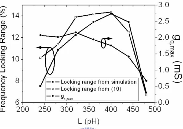
The results of Ansoft Nexxim simulation involving the frequency locking ranges with various inductances are shown in Fig. 2.6. In the simulation, the center output frequency is around 70GHz, the input amplitude is 0.6V, the input NMOS size is 3.6μm/0.12μm, and the minimum required output voltage amplitude is 250mV. The
gq,max value in each case is obtained from Fig. 5, so the locking range can be given by
(2.10). Fig. 2.6 also plots the gq,max value and the locking range given by (2.10), which
are consistent with the simulation results.
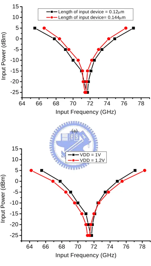
Because the input device is small (i.e. 3.6μm/0.12μm), the size variation of the input device should be considered in the circuit design. Fig. 2.7(a) shows the simulation results when the length of input device varies from 0.12μm to 0.144μm (i.e. 20% variation). When input power is 5dBm, the locking range deceases from 11.6GHz to 9.6GHz and the corresponding percentage is from 16.3% to 13.5%. It can be observed that because the locking range is significantly extended by the proposed
circuit structure, even 20% variation of the input device is considered, the locking range still can be maintained above 10%.
In order to integrate with other 0.13-μm CMOS circuit, Fig. 2.7(b) shows the simulation results when the supply voltage increases to 1.2V. It should be noted that the direct ILFDs in both cases in Fig. 2.7(b) have the same DC current. The simulation results show that, for any input power, the locking ranges increase when VDD increases to 1.2V because the overdrive voltage of the input device increases. This is consistent with the analysis results. When the input power is 5dBm, the locking range increases from 11.6 to 14.1GHz (i.e. from 16.3% to 20.6%).
2.2.5 To Integrate with a differential VCO
There are 2 general methods to integrate single-ended input ILFD with a differential VCO:
1) If a quadrature output signal is required, two independent ILFDs with single-ended input can be directly integrated with a differential VCO [26] 2) If only a differential output signal is required, a dummy input device can be
used to balance the differential VCO to reduce the phase and amplitude error [92].
2.3 PHASE NOISE ANALYSIS
In this section, the noise model in an earlier work [26] is modified and used to analysis the phase noise of a direct ILFD. The block diagram of a direct ILFD is redrawn in Fig. 2.8(a) with the active Gm cell replaced by a negative resistor -Ract. Iin,ω
(
)
(
)
(
out in out)
amp in amp in in t i t i I ϕ ϕ γ ϕ ω α ω ω − + + = + = 2 cos cos , , , (2.12)where iin,amp is the amplitude of Iin,ω and α is the phase of Iin,ω which can be
decomposed to φout and the extra phase γ. Here γ is related to the phase difference
between the input and output voltage signal, and so it can be given as a function of
φin/2-φout.
Fig. 2.8(b) presents the linear loop for the phase noise analysis, where φn_in and
φn_out are the random variables that represent the small phase fluctuations of the input
and output voltage signals. Here Z(ωm) represents the small phase response of the
equivalent load in Fig. 2.8(a) and is given by
( )
o m eq m jQ Z ω ω ω 2 1 1 + = (2.13)where Qeq ≈ (Ract-R)/ωoL is the quality factor of the equivalent load and ωm = ω-ωo is
the offset frequency. The values of the partial differentiations in Fig. 2.8(b) can be easily calculated using
⎟ ⎠ ⎞ ⎜ ⎝ ⎛ − = ∂ ∂ out in in ϕ ϕ γ ϕ α 2 1 ' 2 1 (2.14) and ⎟ ⎠ ⎞ ⎜ ⎝ ⎛ − − = ∂ ∂ out in out ϕ ϕ γ ϕ α 2 1 ' 1 (2.15)
where γ’ is the derivative of γ. From (2.13) to (2.15), the transfer function of the input and output phase noise spectral densities, Sφn_in and Sφn_out respectively, is given
by
( )
( )
(
)
2 _ _ 1 4 1 P m m in n m out n S S ω ω ω ω ϕ ϕ + = (2.16) where(
)
. 2 2 1 ' 2 2 1' in out Qeq o2 in out L Ract R o P ⎟ − ⎠ ⎞ ⎜ ⎝ ⎛ − ≈ ⎟ ⎠ ⎞ ⎜ ⎝ ⎛ − =ω γ ϕ ϕ ω γ ϕ ϕ ω (2.17)
For a stable oscillating signal, Ract is equal to R+Rin. Therefore, (2.17) can be
rewritten as . 2 1 2 1 ' 2 ⎟ ⎠ ⎞ ⎜ ⎝ ⎛ − ⎟ ⎠ ⎞ ⎜ ⎝ ⎛ − ≈ o o in out i out in P ω v γ ϕ ϕ L I ϕ ϕ ω (2.18)
The calculation of the transfer function of the free running and output phase noise spectral densities (Sφn_free-run and Sφn_out) is as in an earlier cited work [26]; only the
result is shown here:
( )
( )
1(
(
)
)
2. 2 _ _ P m P m m run free n m out n S S ω ω ω ω ω ω ϕ ϕ + = − (2.19)From (2.16), the input phase noise appears at the output with a 6-dB reduction and low-pass shaping, dominating the output phase noise when the offset frequency is less than ωP. When the offset frequency exceeds ωP, then from (2.19), the output phase
noise is dominated by the phase noise of the divider in free-run. This result is similar to that of a conventional ILFD. The simulated curves of Sφn_out/Sφn_in with various ωo,
Vov and vin at the central frequency are plotted in Fig. 2.9. From Fig. 2.9, ωP/2π
Therefore, with respect to noise, this structure is also suitable for MMW operations because as ωo becomes large, its internal noise can be suppressed even at a large
offset frequency.
2.4 EXPERIMENTAL RESULTS
The proposed ILFD shown in Fig. 2.5 is designed and fabricated using 0.13μm bulk CMOS technology with a supply voltage of 1V. The size of the Min is only
3.6μm/0.12μm. Based on the proposed design guidelines, Q factor of the passive load should be designed as large as possible. Therefore, any finite resistor in parallel with
L degrades the locking range and power consumption. Here, a low-Q ILFD with a
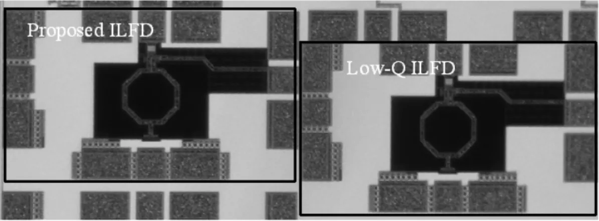
resistor around 1kΩ connected in parallel with L to reduce the Q factor is also fabricated on the same chip to observe the relationship between the locking range and the Q factor. The low-Q ILFD circuit schematic is shown in Fig. 2.10 where Rp = 1kΩ.
The chip micrographs of both fabricated ILFDs are shown in Fig. 2.11.
The measurement setups for input power and ILFD measurement are shown in Fig. 2.12(a) and (b) respectively. After the losses from the cable and the buffer have been de-embedded, the measured output amplitudes versus the input frequencies for the various values of IDC are presented in Fig. 2.13(a). The locking range can be
determined by the difference between the frequencies at the two ends of each curve in Fig. 2.13(a). Fig. 2.13(b) plots the curves of the locking range and the minimum output amplitude in throughout the locking range, versus IDC. The simulated and
calculated curves are also shown for comparison. Possible sources of the error between the calculation and simulation are: 1) distributed effect of the passive load is not considered; 2) the output voltage amplitudes are different at lower and higher locking range due to the distributed effect; and 3) harmonic output components are