國 立 交 通 大 學
電子工程學系 電子研究所
碩 士 論 文
在二氧化鉿為基底之高介電係數閘極介電層中的
載子捕捉與逃逸的電性行為
Charge Trapping and De-trapping Behaviors
in Hf-Base High-k Gate Dielectrics
研 究 生:詹効諭
指導教授:簡昭欣 博士
在二氧化鉿為基底之高介電係數閘極介電層中的
載子捕捉與逃逸的電性行為
Charge Trapping and De-trapping Behaviors
in Hf-Base High-k Gate Dielectrics
研 究 生:詹効諭 Student:Shiao-Yu Chan
指導教授:簡昭欣 博士 Advisor:Dr. Chao-Hsin Chien
國立交通大學
電子工程學系 電子研究所
碩士論文
A Thesis
Submitted to Department of Electronics Engineering and Institute of Electronics
College of Electrical and Computer Engineering National Chiao Tung University
in partial Fulfillment of the Requirements for the Degree of
Master
In Electronics Engineering August 2008
Hsinchu, Taiwan, Republic of China
在二氧化鉿為基底之高介電係數閘極介電層中的
載子捕捉與逃逸的電性行為
研究生:詹効諭 指導教授:簡昭欣 博士
國立交通大學
電子工程學系 電子研究所
摘要
隨著 CMOS 技術急速的微縮到奈米技術點,傳統以二氧化矽或氮氧化矽為閘極 介電層將達到物理與電性的極限。主要的問題是量子效應引發的直接穿隧電流, 導致無法接受的大量載子穿隧超薄的氧化層。高介電係數的材料當閘極介電層, 它可以提供較厚的物理厚度並且得到想要的等效電性氧化層厚度,而二氧化鉿為 基底的高介電係數閘極介電層已經被認為最有希望的替補者。不過,以二氧化鉿 為基底的高介電係數閘極介電層具有相當嚴重的可靠度問題—臨界電壓的不穩定 性,起因於高介電層早已存在的主體缺陷中的載子捕捉與逃逸現象。另一方面, 我們也可以利用一些方法來減緩元件的微縮,而遷移率的增加最有用的方法之 一。遷移率增加的技術提供了有效且必要的方法,讓操作電壓和功率的輸出降低, 而不會失去電路的表現。首先,高拉應力的接觸蝕刻停止層(contact etch stop layer (CESL)),對 N 型金氧半場效電晶體可以很明顯的增加電子的遷移率和打開的電流,而且它是最 熱門的遷移率增加技術之一。所以我們會探討,拉應力效應在 N 型金氧半場效電
晶體的基本的電性特性和載子捕捉的情形。再來,利用適合(fit)臨界電壓的偏移 對施加應力(stress)/恢復(recovery)時間的數據,我們可以研究,在 N 和 P 型金 氧半場效電晶體,載子捕捉和逃逸的物理機制。最後,我們要討論,氟的效應在 P 型金氧半場效電晶體的基本的電性特性和負偏壓高溫度不穩定性(negative bias temperature instability,NBTI) 。此外,我們利用脈波 I-V 的量測方法,來研 究快速載子捕捉的情形。
Charge Trapping and De-trapping Behaviors
in Hf-Base High-k Gate Dielectrics
Student:Shiao-Yu Chan Advisor:Dr. Chao-Hsin Chien
Department of Electronics Engineering and Institute of Electronics
National Chiao Tung University
Abstract
As COMS devices are scaled aggressively into nanometer regime, the conventional SiO2 or SiON gate dielectrics are approaching their physical and electrical limits. The major issue is the intolerably huge leakage current caused by the direct tunneling of carriers through the ultrathin oxide. High permittivity materials as gate dielectrics have been proposed to offer thicker dielectric physical thickness with the desired equivalent oxide thickness in electrical properties and Hf-base high-k gate dielectrics have been recognized as the most promising candidates. However, the Hf-based high-k gate dielectrics are known to suffer from the reliability concern of threshold voltage instability due to the charge trapping and de-trapping in the pre-existing bulk traps in Hf-based high-k gate dielectrics. On the other hand, in order to retard the downscaling of Si based CMOS device, mobility enhancement is one of the most useful methods. Mobility enhancement techniques represent an effective and essential way to reduce Vdd and resulting power consumption without losing circuit performance.
tensile-stress contact etch stop layer (CESL), which can obviously improve electron mobility and ION for nMOSFETs. The basic electrical properties and the charge trapping condition of strain effect are investigated in nMOSFETs. Next, the physical mechanisms of charge trapping and de-trapping can be investigated by fitting the data of the threshold voltage shifts versus stress/recovery time in nMOSFETs and pMOSFETs. Final, the basic electrical properties and the negative bias temperature instability of fluorine effect are investigated in pMOSFETs. Moreover, the fast charge trapping is investigated by pulsed I-V measurement.
誌 謝
這本論文能夠完成,首先我要感謝我的指導老師 簡昭欣 博士。老師提供給 我們充足的研究資源,讓我們能夠無後顧之憂的前進;而老師對研究的認真跟嚴 謹的態度,也讓我受益良多。 世璋學長,謝謝你能耐心的指導我,使我具備獨立研究的能力,並且與我一 起討論研究上所遭遇的任何問題,協助我去解決它們。感謝 NDL 的高頻實驗室裡 的工程師們與計測實驗室裡的彭作煌先生在量測分析儀器上的幫助,讓我能夠順 利地完成研究。 謝謝實驗室的學長姐們 明瑞、志彥、兆欽、家豪、峻丞、治國、競之、豐琦、 宜憲和妍心,在實驗上和課業上無私的協助,讓我能很快的步上軌道;感謝其他 要一起畢業的實驗室同學欣哲、宣凱、登偉、敬倫、弘森、猛飛、宇彥,因為有 你們的陪伴,兩年的碩士生活更加充實豐富;感謝學弟們 宗佑、耀陞、政庭、文 朋、柏錡等讓實驗室的氣氛更加融洽。 最後,感謝我的父母,將我栽培長大,有你們一路的支持,讓我能夠堅持到 底,順利畢業;謝謝阿哥,一起念碩士的兩年來,不斷的給我生活上的協助,很 高興能夠跟你一起畢業;謝謝我的鄰居兼親戚的姨丈、阿姨和表哥姐們,總是張 開雙臂歡迎著我回來。Contents
Abstract (Chinese)
--- i
Abstract (English)
---iii
Acknowledgements
---v
Contents
---vi
Table Captions
---ix
Figure Captions
--- x
Chapter 1: Introduction
1.1 Hf-base High-k Gate Dielectric ---1
1.2 Threshold Voltage Instability in the high-k Gate Dielectrics ---2
1.3 Dissertation Organization ---4
Chapter 2: Contact etchant stopping layer in nMOSFETs with
HfO2/SiO2 High-k Gate Stacks
2.1 Introduction ---10
2.2 Device Fabrication ---11
2.3 Basic Characteristic ---11
2.4 Positive Bias Temperature Instability (PBTI) stress ---12
2.5 Pulsed I-V Techniques and Fast Trap Behaviors ---14
Chapter 3: Bias Temperature Instability in nMOSFETs with
HfO2/SiON High-k Gate Stacks
3.1 Introduction ---28
3.2 Device Fabrication ---29
3.3 Electron trapping behaviors during stress in high-k gate dielectric ---29
3.4 Electron De-trapping Behavior during the Stress/Recovery Cycles in
High-k Gate Dielectric ---33
3.5 Fast Electron Trapping Behavior in High-k Gate Dielectric ---36
3.6 Summary ---37
Chapter 4: Constant Voltage Stress and Negative Bias
Temperature Insatiability Stress in pMOSFETs with
HfO2/SiON High-k Gate Stacks and the Effects of Fluorine
incorporation
4.1 Introduction ---55
4.2 Device Fabrication ---56
4.3 Hole Trapping Behaviors during Stress in High-k Gate Dielectric ---56
4.4 Hole De-trapping Behavior during the Stress / Recovery Cycles in
High-k Gate Dielectric ---58
4.5 Fluorine Incorporation ---59
4.5 Fluorine Incorporation ---60
Chapter 5: Conclusions and Suggestions for Future Work
5.1 Conclusions ---77
5.2 Suggestions for Future Work ---78
Table Captions
Chapter 1
Table 1-1 Summarized material and electrical properties of various selected high-k gate dielectrics. ---8
Chapter 3
Table 3-1 The three parameters, ΔVmax, τc0, and γ, extracted by fitting under various stress voltages. ---39
Figure Captions
Chapter 1
Fig.1-1 (a) High-Performance Logic: Jg,limit versus simulated gate leakage current density for SiON gate dielectric. (b) LSTP: Jg,limit versus simulated gate leakage current density for SiON gate dielectric. ---7 Fig 1-2 Bandgap and band alignment of various high-k gate dielectrics with respect to
silicon. The dashed line represents 1 eV above/below the conduction/valence bands, which indicate the minimum barrier height to suppress the gate leakage current. ---9
Chapter 2
Fig. 2-1 The structure of the devices in strained and unstrained samples. ---18 Fig. 2-2 (a) Id-Vg and (b) Gm-Vg curves of nMOSFET with dual-layer HfO2/SiON high-k gate stack in different capping nitride layers. ---19 Fig. 2-3 Id-Vd curves of nMOSFETs with dual-layer HfO2/SiON high-k gate stack in
different thickness of capping nitride layers. ---20 Fig. 2-4 Icp-Vbase curves of nMOSFETs with dual-layer HfO2/SiON high-k gate stack in different thickness of capping nitride layers. ---20 Fig. 2-5 Gm,max-Lgate curves of nMOSFETs with dual-layer HfO2/SiON high-k gate stack in different thickness of capping nitride layers. ---21 Fig. 2-6 Threshold voltage shift of nMOSFETs as a function of the stress time in
difference thickness of capping nitride layers. ---22 Fig. 2-7 ln(JG/Eeff) as a function of Eeff1/2 in the (a) unstrained and (2) strained devices.
Fig. 2-8 ln(JG/Eeff) as a function of Eeff1/2 in the unstrained and strained devices. The barrier heights can be obtained by the slopes. ---24 Fig. 2-9 The drain current degradation of nMOSFETs as a function of the
stress/recovery time with a fixed stress/recovery voltage +2.0V/0V in difference thickness of capping nitride layers. ---25 Fig. 2-10 Id-Vd curves of (a) unstrained (b) SiN = 200nm (c) SiN = 300nm devices by
two measurement methods: DC ramp and pulsed I-V and (d) the distribution of drain current degradation under different conditions. ---26 Fig. 2-11 Id,sat as a function of stress time ranging several nanoseconds to 100ns by
single pulse measurement. ---27
Chapter 3
Fig. 3-1 (a) the gate leakage current density and (b) the subthreshold slop as a function of stress time for nMOSFETs under static stress at various gate bias voltages.---40 Fig. 3-2 The threshold voltage shift as a function of stress time for nMOSFETs under
static stress at various gate bias voltages. ---41 Fig. 3-3 The characteristic capture time constant under various gate bias voltages. ----41 Fig. 3-4 The trapped charge density distribution versus capture time under different
stress voltages. ---42 Fig. 3-5 The ratio of early traps to fast traps under various gate bias voltages. ---42 Fig. 3-6 The drain current degradation as a function of stress time for nMOSFETs under static stress at various gate bias voltages. ---43 Fig. 3-7 (a) The threshold voltage shift as a function of stress time for HfAlO high-k gate dielectric under static stress at various gate bias voltages. (b) The characteristic capture time constant under various gate bias voltages. ---44
Fig. 3-8 The threshold voltage shift as a function of stress time for nMOSFETs under static stress at various temperatures. ---45 Fig. 3-9 The charge pumping current as a function of base voltage of fresh and stressed
conditions under various stress temperatures. ---45 Fig. 3-10 The threshold voltage shift as a function of stress time for nMOSFETs under static stress at various dimensions. ---46 Fig. 3-11 The drain current degradation (ΔId,sat/ Id0,sat) can be linearly transformed with the threshold voltage shift (ΔVT). ---47 Fig. 3-12 The drain current degradation for nMOSFETs under static stress/recovery time
with a fixed stress voltage Vg=+2.0V and various recovery voltages Vg =+1.4 ~-1.4V. ---48 Fig. 3-13 (a) The threshold voltage shift as a function of stress time for HfO2 high-k
gate dielectric under recovery at various recovery voltages. (b) The characteristic emission time constant under various recovery voltages. ---49 Fig. 3-14 The trapped charge density distribution versus capture time under different
stress voltages. ---50 Fig. 3-15 The drain current degradation for nMOSFETs under static stress / recovery
time with various voltages Vg= +1.5~2.5V and a fixed recovery voltage Vg = 0V. ---51 Fig. 3-16 (a) The threshold voltage shift as a function of stress time for HfO2 high-k
gate dielectric under recovery at various stress voltages. (b) The characteristic emission time constant under various stress voltages. ---52 Fig. 3-17 The drain current degradation for nMOSFETs under static stress/recovery time
with a fixed stress voltage Vg=+2.0V and various recovery voltages Vg =+0.7 ~-2.0V. ---53 Fig. 3-18 Id-Vd curves under (a) 25℃ (b) 50℃ (c) 75℃ (d) 125℃ by two measurement
methods: DC ramp and pulsed I-V. ---54
Chapter 4
Fig. 4-1 The charge pumping current as a function of top voltage of fresh and stressed conditions. ---63 Fig. 4-2 (a) The threshold voltage shift as a function of stress time for HfO2 high-k gate
dielectric under static stress at various gate bias voltages. (b) The characteristic capture time constant under various gate bias voltages. ---64 Fig. 4-3 The threshold voltage shift as a function of stress time for pMOSFETs under
static stress at various temperatures. ---65 Fig. 4-4 The charge pumping current as a function of top voltage of fresh and stressed
conditions under various stress temperatures. ---65 Fig. 4-5 The threshold voltage shift for pMOSFETs under static stress/recovery time
with a fixed stress voltage Vg=-2.0V and various recovery voltages Vg =0~ 1.0V. ---66 Fig. 4-6 (a) The threshold voltage shift as a function of stress time for HfO2 high-k gate
dielectric under recovery at various recovery voltages. (b) The characteristic emission time constant under various recovery voltages. ---67 Fig. 4-7 The threshold voltage shift for pMOSFETs under static stress/recovery time
with various recovery voltages Vg=-2.0~-3.0V and a fixed stress voltage Vg =1.0V. ---68 Fig. 4-8 (a) The threshold voltage shift as a function of stress time for HfO2 high-k gate dielectric under recovery at various stress voltages. (b) The characteristic emission time constant under various stress voltages. ---69 Fig. 4-9 (a) Id-Vg and (b) Gm-Vg curves of pMOSFETs with dual-layer HfO2/SiON high-k gate stack in the devices with fluorine and without fluorine. ---70
Fig. 4-10 Id-Vd curves of pMOSFETs with dual-layer HfO2/SiON high-k gate stack in the devices with and without fluorine. ---71 Fig. 4-11 Icp-Vtop curves of nMOSFETs with dual-layer HfO2/SiON high-k gate stack in the devices with and without fluorine. ---71 Fig. 4-12 The threshold voltage shift as a function of stress time for pMOSFETs under NBT stress in the devices with and without fluorine. ---72 Fig. 4-13 The charge pumping current under fresh and stressed conditions in the devices
with and without fluorine. ---73 Fig. 4-14 Nonalized high-k trap density (NHK(stressed)/ NHK(fresh)) as a function of
frequency in the devices with and without fluorine. ---74 Fig. 4-15 Id-Vd curves under (a) 25℃ (b) 50℃ (c) 75℃ (d) 125℃ by two measurement methods: DC ramp and pulsed I-V. ---75 Fig. 4-16 Id-Vd curves in the devices (a) without and (b) with fluorine by DC ramp and
pulsed I-V measurement. Id-Vd curves in the device (c) without fluorine and (d) with fluorine after stress by DC ramp and pulsed I-V measurement. ---76
Chapter 1
Introduction
1.1 Hf-base High-k Gate Dielectrics
According to Moore’s law, the continuous downscaling of the dimension of Si based CMOS device has approaching the physical limit of conventional SiO2-based ultrathin
oxides. In recent years, the equivalent oxide thickness of silicon oxynitride SiON has reduced below 2.0 nm that lead to the serious concerns gate dielectric integrity, reliability issues, and stand-by power consumption. However, one of the major challenges to overcome is the rapidly-increasing tunneling gate leakage current with the downscaling of the equivalent oxide thickness. From ITRS roadmap in Fig. 1-1 [1], the two Jg of LSTP and high-performance logic curves cross shortly before or at 2008, and hence, for 2008 and beyond, the leakage current limit cannot be met using silicon oxy-nitride because of direct tunneling.
In order to solve the tunneling current and power consumption in the ultrathin oxides, high permittivity materials as gate dielectrics have been proposed to offer thicker dielectric physical thickness with the desired equivalent oxide thickness in electrical properties. Table 1-1 summarizes the electrical properties of several high-k materials [2], and Fig. 1-2 the bandgap and band offset of these high-k materials with respect to Si [3]. Among these investigated high-k gate dielectrics, Hf-base high-k gate dielectrics have been recognized as the most promising candidates due to their moderate dielectric constant (20~25), large energy bandgap (5.7~6.0eV), high conduction band offset (1.5~1.9eV), excellent thermal stability on the Si substrate (950℃). However, several issues in high-k technology are believed to retard its development such as
mobility degradation as a result of soft optical phonon scattering and threshold voltage instability by charge trapping and de-trapping.
On the other hand, mobility enhancement techniques represent an effective and essential way to reduce Vdd and resulting power consumption without losing circuit
performance. One of the most popular technologies is using high tensile-stress contact etch stop layer (CESL), which can obviously improve electron mobility and ION for
nMOSFETs [4].
1.2 Threshold Voltage Instability in the High-k Gate Dielectrics
Compared with SiO2 and SiON, there are plenty of pre-existing bulk traps in the
high-k gate dielectrics, and this is an intrinsic issue related to specific properties or crystal structure of high-k gate dielectrics, despite the deposition technique or process condition. Because of this characteristic, the pre-existing high-k bulk defects could lead to undesired transport through the dielectrics inducing gate leakage. Moreover, charge trapped by these defects would cause the continued threshold voltage shift, drain current and transconductance degradation during operation. As the gate bias is positive (negative), the injected electrons (holes) through the interfacial oxide would be trapped by the pre-existing bulk defects of the HfO2 layer. As the gate bias is negative (positive),
these trapped electrons (holes) would be relaxed through the interfacial oxide to the Si conduction band in high-k nMOSFETs.
According to the threshold voltage shift and the drain current degradation of the high-k devices during operation, we could build the models which can fit the experiment results and conform to the physical mechanisms of charge trapping and de-trapping. There have been many models built in recent years. Zafar et al. predicted that Vt would shift with power law dependence in the initial stages of stressing whereas
Vt would become constant at long stressing times [5]. Shanware et al. predicted that Vt would shift with logarithmic dependence [6]. These models above would be built by static Id-Vg measurement, and therefore the detected charge carriers in high-k gate dielectrics would only belong to slow traps.
As has been reported recently, the charge trapping in high-k gate dielectrics comprise slow and fast trapping processes. The slow high-k traps have been widely discuss from the hysteresis of C-V curves and the threshold voltage shift of static Id-Vg characteristics. Moreover, the fast high-k traps have been proposed to investigate by the pulse I-V technique and charge pumping method. It is reported that the fast electron trapping is a significant source of device DC performance degradation [7]. The fast high-k traps can instantly capture and emit the charge carriers by tunneling through the thin interfacial oxide [8]-[11]. The tunneling model through the thin interfacial oxide is similar to that of tunneling into near-interface oxide traps in the heavily-irradiated SiO2
that has already been studied and proposed [12] [13]. These near-interface oxide traps are defined as the oxide traps located near the interface that can instantly exchange charge carriers with underlying Si substrate through direct tunneling [14] [15].
This thesis will concentrate on analyzing the data to better understand the fundamental characteristic and the physical mechanisms of charge trapping and de-trapping in Hf-based high-k gate dielectrics. Moreover, the strain effect and the fluorine effect are also investigated completely.
1.3 Dissertation Organization
The organization of this dissertation is briefly described below. Chapter 2 studies the basic characteristics and reliability discussion of strain effect by CESL. The fast trap behavior is discussed under strain effect. Chapter3 discusses the electron trapping and de-trapping behavior under positive bias temperature instability (PBTI) and dynamic PBTI stress. The electron trapping/de-trapping model and the meaning of the parameters by fitting are discussed. The fast trap in nMOSFETs is discussed under various temperatures. Chapter 4 discusses the hole trapping and de-trapping behavior under constant voltage stress (CVS) and recovery. The hole trapping/de-trapping model and the meaning of the parameters by fitting are discussed. The basic characteristics and negative bias temperature instability discussion of fluorine effect are discussed. The fast trap in pMOSFETs is discussed under various temperatures and fluorine effect.
References
[1]“INTERNATIONAL TECHNOLOGY ROADMAP FOR SEMICONDUCTORS: PROCESS INTEGRATION, DEVICES, AND STRUCTURES, “ITRS 2007 edition.
[2] H.-S. P. Wong, “Beyond the conventional transistor,” IBM J. RES. & DEV. VOL. 46 NO. 2/3 MARCH/MAY 2002
[3] J. Robertson, “Band Offsets of Wide-Band-Gap Oxides and Implications for Future Electronic Devices,” J. Vac. Sci. Technol. B 18, 1785–1791 (2000).
[4] S. Pidin et al., “A Novel Strain Enhanced CMOS Architecture Using Selectively Deposited High Tensile and High Compressive Silicon Nitride Films,” IEDM 04-213
[5] Sufi Zafar, Alessandro Callegari, Evgeni Gusev, and Massimo V. Fischetti, “Charge trapping related threshold voltage instabilities in high permittivity gate dielectric stacks,” J. Appl. Phys., Vol. 93, No. 11, 1 June 2003
[6] A. Shanware, M. R. Visokay, J. J. Chambers, A. L. P. Rotondaro, H. Bu, M. J. Bevan, R. Khamankar, S. Aur, P. E. Nicollian, J. McPherson, L. Colombo, “Evaluation of the Positive Biased Temperature Stress Stability in HfSiON Gate Dielectrics,” IEEE 03CH37400. 4isl Annual lnlemafional Reliability Physics Symposium, Dallas, Texas, 2003
[7] C. D. Young, R. Choi, J. H. Sim, B. H. Lee, P. Zeitzoff, Y. Zhao, K. Matthews, G. A. Brown, and G. Bersuker, “Interfacial layer dependence of HfSixOy gate stacks
on VT instability and charge trapping using ultra-short pulse in characterization,”
IEEE 05CH37616 43" Annual International Reliability Physics Symposium. San Jose, 2005
[8] A. Kerber, E. Cartier, L. Pantisano, M. Rosmeulen, R. Degraeve, T. Kauerauf, G. Groeseneken, Senior Member, U. Schwalke, “Characterization of the Vt-instability
un SiO2 HFO2 gate dielectrics,” International Reliability Physics Symposium, Dallas, Texas, 2003
[9] L. Pnatisano et al., “Dynamics of threshold voltage instability in stacked high-k dielectrics: role of the interfacial oxide,” 2003 Symposium on VLSl Technology Digest of Technical Papers
[10] C. Leroux, J. Mitard, G. Ghibaudo, X. Garros, G. Reimbold, B. Guillaumot, F. Martinl, “Characterization and modeling of hysteresis phenomena in high K dielectrics,” IEDM 04-737
[11] C. Shen, M. F. Li, X. P. Wang, H. Y. Yu, Y. P. Feng, A. T.-L. Lim, Y. C. Yeo, D. S. H. Chan, D. L. Kwong, “Negative U Traps in HfO2 Gate Dielectrics and Frequency
Dependence of Dynamic BTI in MOSFETs,” IEDM 04, pp. 733-736
[12] Y. Maneglia and D. Bauzaa, “Extraction of slow oxide trap concentration profiles in metal–oxide–semiconductor transistors using the charge pumping method,” J. Appl. Phys. 79 (8), 15 April 1996
[13] Theodore L. Tewksbury, and Hae-Seung Lee, “Characterization, modeling, and minimization of transient threshold voltage shifts in MOSFETs,” IEEE JOURNAL OF SOLID-STATE CIRCUITS, VOL. 29, NO. 3, MARCH 1994.
[14] R. E. Paulsen, R. R. Siergiej, M. L. French, and M. H. White, “Observation of near-interface oxide traps with the charge-pumping technique,” IEEE ELECTRON DEVICE LETTEKS, VOL. 13, NO. 12, DECEMBER 1992
[15] Ronald E. Paulsen, and Marvin H. White, “Theory and application of charge pumping for the characterizationof Si-SiO2 interface and near-interface oxide traps,” IEEE TRANSACTIONS ON ELECTRON DEVICES, VOL. 41, NO. 7, JULY 1994
(a) High-Performance Logic: Jg,limit versus simulated gate leakage current
density for SiON gate dielectric. (b) LSTP: Jg,lim Fig.1-1
it versus simulated gate leakage current density for SiON gate dielectric. [1]
Table 1-1 terial and electrical properties of various selected high-k gate dielectrics [2].
Fig 1-2 Bandgap and band alignment of various high-k gate dielectrics with respect to silicon. The dashed line represents 1 eV above/below the conduction/valence bands, which indicate the minimum barrier height to suppress the gate leakage current [3].
Chapter 2
Contact etchant stopping layer in nMOSFETs
with HfO
2/SiO
2High-k Gate Stacks
2.1 Introduction
As conventional SiO2-based ultrathin oxides are scaling down, the rapidly-increasing
tunneling gate leakage current has been a major challenge. In order to retard the downscaling of Si based CMOS device, mobility enhancement is one of the most useful methods. Mobility enhancement techniques represents an effective and essential way to reduce Vdd and resulting power consumption without losing the circuit performance, relieving the burden of gate dielectric scaling. There are many methods of mobility enhancement: a) channel-strain engineering, b) substrate and channel orientations ((100) or (110)), and c) new channel materials (SiGe, Ge and III-V). The channel-strain engineering comprises biaxial and uniaxial strain (tensile or compressive). The biaxial tensile strain uses the technique of the so-called SiGe-relaxed buffer or virtual substrate [1]-[3]. Recently, this technique has also been successfully implemented on SOI wafers [4]. In contrast, it is difficult to fabricate a biaxial compressive strain in silicon; it’s very beneficial effect to holes has been demonstrated with SiGe channels in [5]. The uniaxial tensile strain in the channel can be produced with SiC epitaxial source–drain regions and with the contact-etch-stop-layer (CESL) nitride layer. The uniaxial compressive strain can be obtained with SiGe epitaxial source–drain regions [6], with a SiGe stressor located under the channel region [7], and with CESL. The contact-etch stop layer nitride layer can induce both tensile strain for nMOSFETs and compressive strain for pMOSFETs, so that dual stress liner with SiN capping is one of the most popular
techniques of mobility enhancement.
In this chapter, the high-k nMOSFETs with the contact-etch-stop-layers that induce tensile strain in the channel are introduced. The strain effect can be realized by basic characteristics in section 2.3. In section 2.4, the difference of the charge trapping between the stained and unstrained devices will be studied during the positive bias stress. Finally, the transient charge carriers in stain effect will be analyzed by pulsed I-V techniques in section 2.5.
2.2 Device Fabrication
nMOSFET devices with the poly-Si/HfO2/SiON high-k gate stacks were fabricated
using the standard CMOS process technology. The interfacial oxide (~1.0 nm) was formed by oxide rapid thermal anneal (RTA) at 800℃ in N2O ambient with 30s,
followed by the deposition of the HfO2 (~3.0 nm) high-k gate dielectric using atomic
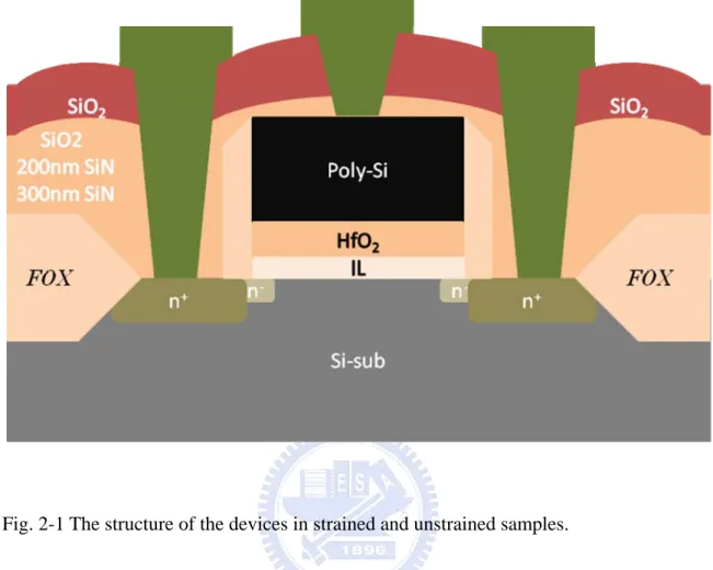
layer deposition (ALD) technique. The 200 nm poly-Si was deposited by low pressure chemical vapor deposition (LPCVD). After gate definition, spacer formation, and S/D implantation, the tensile strain induced by SiN capping layer was deposited by plasma chemical vapor deposition (PECVD). The capping nitride layers were divided into three kinds of thickness such as 200 nm, 300 nm and without SiN. The equivalent oxide thickness of above mentioned high-k gate stack was extracted to be 2.0~2.5 nm by using C-V measurement. The structure of the devices are shown in Fig. 2-1
2.3 Basic Characteristic
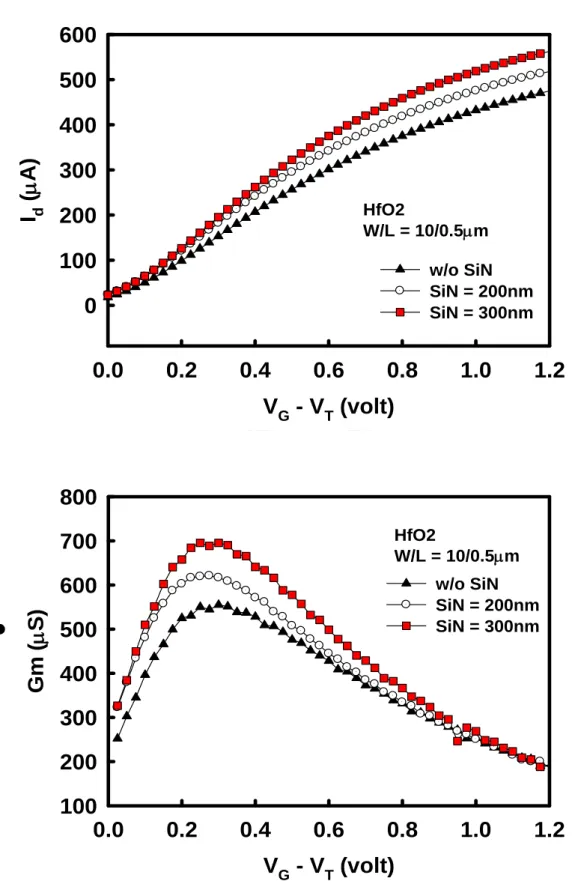
Fig. 2-2 (a) (b) show Id-Vg and Gm-Vg curves of nMOSFETs with dual-layer
Id-Vg curves, as the thickness of capping nitride layer was thicker, drain current would be larger. In Gm-Vg curve, the same phenomenon would also be occurred. Turn-on
current which varies with gate voltage also represented larger in thicker nitride layer in Fig. 2-3. The reason of improvement of the stained devices is mobility enhancement as a result of electron effective mass. The channel stressed by capping nitride layer would induce the electrons of 2-fold valley with lighter transport effective mass to increase. As the inverted electrons with lighter effective mass increase, the mobility of the strained devices will enhance. Fig. 2-4 shows Icp-Vbase curves by charge pumping method of
nMOSFETs with dual-layer HfO2/SiON high-k gate stack in different thickness of
capping nitride layers. From Icpmax of Icp-Vbase curves, the interface trap density could be
obtained. Moreover, the interface trap density of the strained devices was smaller than that of the unstrained device because of hydrogen passivation by capping nitride layers of PECVD. From Fig. 2-5, the Gm,max enhancement could decrease with gate length
increasing because of CESL belonged to local strain [8].
2.4 Positive Bias Temperature Instability (PBTI) stress
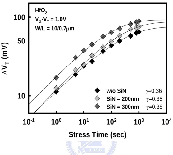
Threshold voltage instability induced by charge trapping has been recognized as one of the critical reliability issues in high-k gate dielectrics, especially for nMOSFETs under substrate electron injection conditions [9]. Fig. 2-6 shows threshold voltage shift of nMOSFETs as a function of the stress time in difference thickness of capping nitride layers. The Vt shift of strained devices showed more serious than that of unstrained
devices. Moreover, thicker capping nitride layers would increase more Vt shift. The
physical mechanism or the modeling of the fitting lines in Fig. 2-6 will be discussed in chapter 3. In order to confirm the reason of the more Vt shift of the strained devices, the
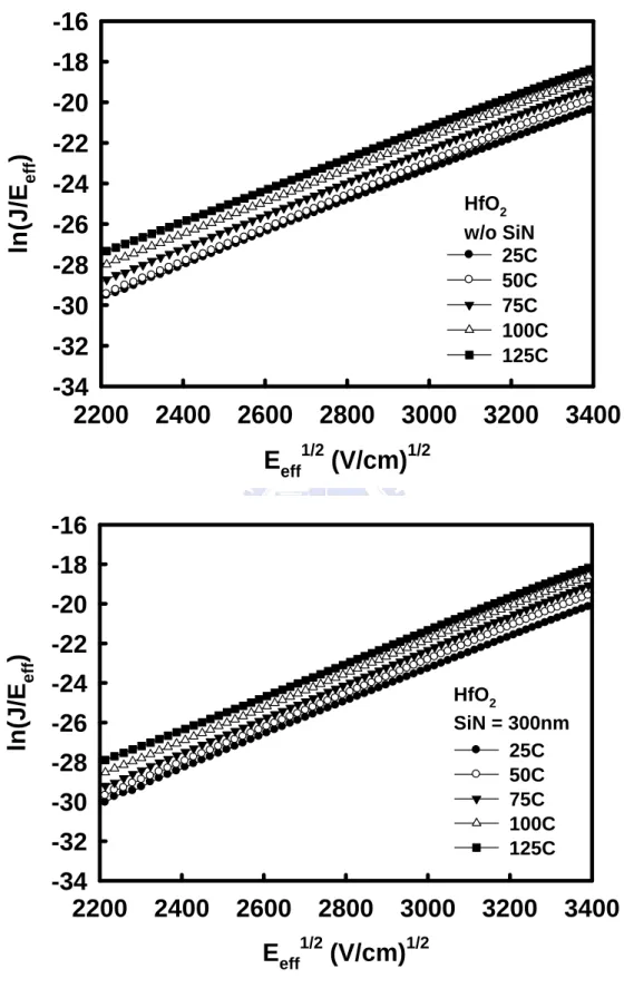
for electrons from Si substrate by Fowler-Nordheim (F-N) tunneling fitting between the unstrained and the strained devices should be extracted. Fig. 2-7 shows ln(JG/Eeff) as a
function of Eeff1/2 in the (a) unstrained and (b) strained devices. The curves of the two
plots followed Frenkel–Poole emission as indicated by a good linear fit to the experimental data. Then, the trapped energy levels could be obtained from the y-axis intercept (Eq. (2.1)). It could be found that almost the same trapped energy levels of the unstrained and strained devices. Fig. 2-8 shows the ln(JG/Eeff) as a function of 1/Eeff in
unstrained and strained devices. The slops of the lines fit to the experiment data could be obtained the barrier height (Eq. (2.2)). The similar slope represented the similar barrier height in unstrained and strained devices. Thus, the trapped energy level and the barrier height for electrons from Si substrate are not change by strain. It can be assumed that the more Vt with increasing capping nitride layer is due to the generated bulk traps
of HfO2 by stain. Moreover, the thicker capping nitride layer represents the more
generated bulk traps of HfO2.
Frenkel-Poole emission: 2 2 2 ; ); / ( exp( 0 HfO SiO T HfO ox T ox B q N a kT aqE q E a B J ε ε μ ε πε = = − Φ − ⋅ ⋅ ⋅ = ⎥⎦ ⎤ ⎢⎣ ⎡ Φ + − − = / ln( ) ) ln( 2 0 aB kT q E kT aq q E J T ox HfO ox ε πε (2.1) F-N tunneling: J ≈ Eox2 ⋅exp(−B Eox) 1/2 2 / 1 * 3 ) 2 ( 8 ) ( =− Φ h qm slope B π (2.2)
Fig. 2-9 shows the drain current degradation of nMOSFETs as a function of the stress/recovery time with a fixed stress/recovery voltage +2.0V/0V in difference thickness of capping nitride layers. From every single line in Fig. 2-9, the charge trapping and de-trapping behavior changed since the trapped charge had not been completely removed at weak recovery voltages during previous recovery cycles. Moreover, the trapped electrons and the residual electrons during stress/recovery time of strained device would induce more drain current degradation than that of unstrained device.
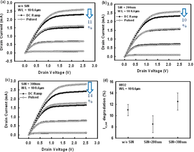
2.5 Pulsed I-V Techniques and Fast Trap Behaviors
Fig. 2-10 shows Id-Vd curves of (a) unstrained (b) SiN = 200nm (c) SiN = 300nm
devices by two measurement methods: DC ramp and pulsed I-V. The measurement time of the conventional DC ramp measurement is about several milliseconds to seconds. The pulse width of the pulsed I-V measurement we used is 100ns and raising/falling time is 20ns. Thus, the different of Id,sat by two methods could be the charge loss with
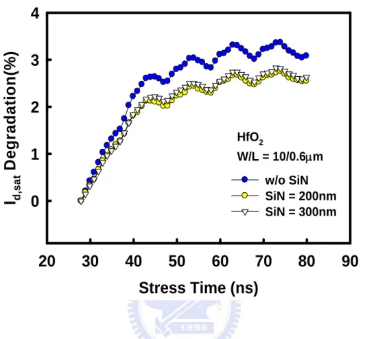
the capture time ranging from 100ns to several milliseconds. The charge loss decreased in thinner capping nitride layer device and increased in thicker capping nitride layer device. The behavior of these fast traps would be a little different from that of the slow traps by PBTI measurement. It can be assumed that the hydrogen passivation is dominant in thinner capping nitride layer device and the trap generation is dominant as the capping nitride layer is thicker. Fig. 2-11 shows Id,sat as a function of stress time
ranging several nanoseconds to100ns by single pulse measurement. The detected traps would be more close to the interface of Si/SiON. Thus, the result are almost the same with the interface state by charge pumping measurement and the reason of the result can be also assumed the hydrogen passivation.
2.6 Summary
The contact-etch-stop-layer (CESL) is one of mobility enhancement methods and it can induce tensile strain to improve mobility for nMOSFETs. In our data, the strained devices could improve the electrical characteristics of NMOS, but they would induce more threshold voltage shift in high-k material. By F-P and F-N tunneling fitting, the trapped energy levels and the barrier heights of stained and unstrained devices are almost the same. Thus, we conclude that the strain effect induces bulk traps generated in HfO2. Form the transient effect by pulsed I-V, the competition of hydrogen passivation
and trap generated by strain can be found. The charge loss detected by single pulsed ranging several nanoseconds of strained and unstrained devices represents the interface states improvement due to hydrogen passivation.
References
[1] J. Welser, J. L. Hoyt, and J. F. Gibbons, “Electron mobility enhancement in strained-Si n-type metal-oxide-semiconductor field-effect transistors," IEEE Electron Device Lett., vol. 15, no. 3, pp. 100–102, Mar. 1994.
[2] J. L. Hoyt, H. M. Nayfeh, S. Eguchi, I. Aberg, G. Xia, T. Drake, E. A. Fitzgerald, and D. A. Antoniadis, “Strained silicon MOSFET technology,” in IEDM Tech. Dig., Dec. 2002, pp. 23–26.
[3] M. Jurczak, T. Skotnicki, G. Ricci, Y. Campidelli, C. Hernandez, and D. Bensahel, “Study on enhanced performance in NMOSFETs on strained silicon,” in Proc. ESSDERC, 1999, pp. 304–307.
[4] C. Mazure, “Advanced substrate engineering for the nanotechnology era,” in Proc. Int. Symp. VLSI Technol., Syst., Appl., 2006, pp. 78–79.
[5] M. L. Lee and E. A. Fitzgerald, “Optimized strained Si/strained Ge dualchannel heterostructures for high mobility P-and N-MOSFETs,” in IEDM Tech. Dig., Dec. 2003, pp. 429–432.
[6] T. Ghani, M. Armstrong, C. Auth, M. Bost, P. Charvat, G. Glass, T. Hoffmann, K. Johnson, C. Kenyon, J. Klaus, B. McIntyre, K. Mistry, A. Murthy, J. Sandford, M. Silberstein, S. Sivakumar, P. Smith, K. Zawadzki, S. Thompson, and M. Bohr, “A 90 nm high volume manufacturing logic technology featuring novel 45 nm gate length strained silicon CMOS transistors,” in IEDM Tech. Dig., Dec. 2003, pp. 978–980. [7] D. Chanemougame, S. Monfray, F. Boeuf, A. Talbot, N. Loubet, F. Payet, V. Fiori, S.
Orain, F. Leverd, D. Delille, B. Duriez, A. Souifi, D. Dutartre, and T. Skotnicki, “Performance boost of scaled Si PMOS through novel SiGe stressor for HP CMOS,” in VLSI Symp. Tech. Dig., 2005, pp. 180–181.
[8] Thomas Skotnicki, Claire Fenouillet-Beranger, Claire Gallon, Frederic Boeuf, Stephane Monfray, Fabrice Payet, Arnaud Pouydebasque, Melanie Szczap, Alexis
Farcy, Franck Arnaud, Sylvain Clerc, Augustin Cathignol, Jean-Pierre Schoellkopf, Ernesto Perea, Richard Ferrant, and Hervé Mingam, “Innovative Materials, Devices, and CMOS Technologies for Low-Power Mobile Multimedia,” IEEE TRANSACTIONS ON ELECTRON DEVICES, VOL. 55, NO. 1, JANUARY 2008. [9] K. Onishi et al. “Bias-temperature instabilities of polysilicon gate HfO2 MOSFETs,”
IEEE TRANSACTIONS ON ELECTRON DEVICES, VOL. 50, NO. 6, JUNE 2003.
HfO2 W/L = 10/0.5μm
V
G- V
T(volt)
0.0
0.2
0.4
0.6
0.8
1.0
1.2
I
d(
μA)
0
100
200
300
400
500
600
w/o SiN SiN = 200nm SiN = 300nm z HfO2 W/L = 10/0.5μmV
G- V
T(volt)
0.0
0.2
0.4
0.6
0.8
1.0
1.2
Gm
(
μS)
100
200
300
400
500
600
700
800
w/o SiN SiN = 200nm SiN = 300nmFig. 2-2 (a) Id-Vg and (b) Gm-Vg curves of nMOSFET with dual-layer HfO2/SiON
VG - VT = 1.0 V VG - VT = 0.75 V VG - VT = 0.5 V VG - VT = 0.25 V
V
d(volt)
0.0
0.5
1.0
1.5
2.0
2.5
3.0
I
d(
μA)
-200
0
200
400
600
800
1000
1200
1400
1600
1800
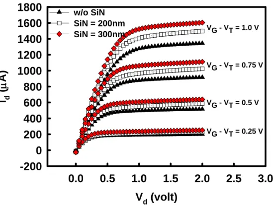
w/o SiN SiN = 200nm SiN = 300nmFig. 2-3 Id-Vd curves of nMOSFETs with dual-layer HfO2/SiON high-k gate stack in
different thickness of capping nitride layers.
HfO2 W/L = 10/4μm
Base Voltage (V)
-2.0
-1.5
-1.0
-0.5
0.0
0.5
1.0
I
cp(n
A
)
-10
0
10
20
30
40
50
w/o SiN SiN = 200nm SiN = 300nmFig. 2-4 Icp-Vbase curves of nMOSFETs with dual-layer HfO2/SiON high-k gate stack in
HfO2
Gate Length (
μm)
1
1
0
Gm
ma x0
200
400
600
800
1000
1200
w/o SiN SiN = 200nm SiN = 300nmFig. 2-5 Gm,max-Lgate curves of nMOSFETs with dual-layer HfO2/SiON high-k gate stack
HfO2
VG-VT = 1.0V W/L = 10/0.7μm
Stress Time (sec)
10
-110
010
110
210
310
4Δ
V
T(m
V
)
50
10
100
w/o SiN γ=0.36 SiN = 200nm γ=0.38 SiN = 300nm γ=0.38Fig. 2-6 Threshold voltage shift of nMOSFETs as a function of the stress time in difference thickness of capping nitride layers.
HfO2 w/o SiN
E
eff1/2(V/cm)
1/22200
2400
2600
2800
3000
3200
3400
ln
(J
/E
ef f)
-34
-32
-30
-28
-26
-24
-22
-20
-18
-16
25C 50C 75C 100C 125C HfO2 SiN = 300nmE
eff1/2(V/cm)
1/22200
2400
2600
2800
3000
3200
3400
ln
(J/E
eff)
-34
-32
-30
-28
-26
-24
-22
-20
-18
-16
25C 50C 75C 100C 125CFig. 2-7 ln(JG/Eeff) as a function of Eeff1/2 in the (a) unstrained and (2) strained devices.
HfO2
1/E (cm/MV)
0.055
0.060
0.065
0.070
0.075
0.080
0.085
ln
(J
/E
)
-37
-36
-35
-34
-33
-32
-31
w/o SiN SiN = 200nm SiN = 300nm fit curveFig. 2-8 ln(JG/Eeff) as a function of Eeff1/2 in the unstrained and strained devices. The
HfO2
W/L = 10/0.4μm
VG - VT = 1.0V ; VR = 0V
Stress/Recovery Time (sec)
0
2000 4000 6000 8000 10000
I
dD
e
gr
e
da
ti
on (
%
)
0
20
40
60
w/o SiNSiN = 300nmFig. 2-9 The drain current degradation of nMOSFETs as a function of the stress/recovery time with a fixed stress/recovery voltage +2.0V/0V in difference thickness of capping nitride layers.
Fig. 2-10 Id-Vd curves of (a) unstrained (b) SiN = 200nm (c) SiN = 300nm devices by
two measurement methods: DC ramp and pulsed I-V and (d) the distribution of drain current degradation under different conditions.
HfO2 W/L = 10/0.6μm
Stress Time (ns)
20
30
40
50
60
70
80
90
I
d,satD
eg
rad
at
io
n
(%
)
0
1
2
3
4
w/o SiN SiN = 200nm SiN = 300nmFig. 2-11 Id,sat as a function of stress time ranging several nanoseconds to 100ns by
Chapter 3
Bias Temperature Instability in nMOSFETs with
HfO
2/SiON High-k Gate Stacks
3.1 Introduction
Threshold voltage instability in Hf-based high-k gate dielectrics has been recognized as one of the most critical reliability issues that need to be solved urgently, especially for the nMOSFETs under substrate electron injection conditions (positive bias stress) [1]. The electrons in channel are injected into the pre-existing bulk traps of the HfO2 high-k gate dielectric by tunneling through the thin interfacial oxide. The pre-existing traps of the HfO2 high-k gate dielectric are positioned above the Si conduction band edge in energy and in the HfO2 bulk layer in space. These pre-existing bulk traps are distributed in a wide range of space and energy [2], thus making the charge trapping model different from that of conventional SiO2 or SiON. Furthermore, the high-k dielectrics are reversible by charge trapping and de-trapping. Thus, it is found that the trapped charge carriers could recover to the pre-stress condition after prolonged recovery time. According to results of the threshold voltage shift and the drain current degradation with stress/recovery time, the model could be built to fit the data with reasonable physical mechanism. However, since the charge carriers could be trapped/de-trapped quickly and easily by applying a forward/reverse bias voltage, the degradation may be underestimated due to the switching and measuring delays in the stress/measure cycles [3]. These so-called fast traps would be detected by transient measurement solving the underestimate of charge trapping in high-k gate dielectrics.
geometrics will be studied in detail to comprehend the physical model in section 3.3. In section 3.4, the charge de-trapping behavior under various stress voltages and recovery voltages will be investigated to build the physical model according to the charge trapping model. Finally, the transient charge trapping behavior will be analyzed by pulsed I-V measurement.
3.2 Device Fabrication
nMOSFET devices with the poly-Si/HfO2/SiON high-k gate stacks were fabricated using the conventional CMOS process technology. The interfacial oxide (~1.0 nm) was formed by oxide rapid thermal anneal (RTA) at 800℃ in N2O ambient with 30s, followed by the deposition of the HfO2 (~3.0 nm) high-k gate dielectric using atomic layer deposition (ALD) technique. The 200 nm poly-Si was deposited by low pressure chemical vapor deposition (LPCVD). After gate definition, spacer formation, and S/D implantation, the capping layer was deposited by plasma chemical vapor deposition (PECVD). The equivalent oxide thickness of above mentioned high-k gate stack was extracted to be 2.0~2.5 nm by using C-V measurement.
3.3 Electron trapping behaviors during stress in high-k gate dielectric
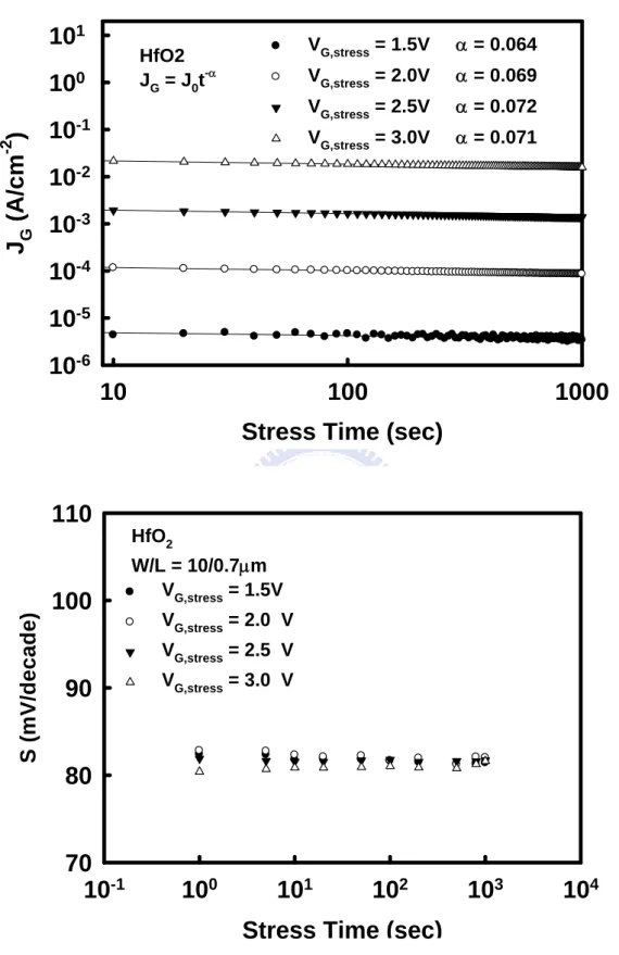
Fig. 3-1 shows (a) the gate leakage current density and (b) the subthreshold slop as a function of stress time for nMOSFETs under static stress at various gate bias voltages. The gate leakage current density increases with stress voltage. The symbols in Fig. 3-1 (a) are the measurement data and the solid lines are power law fits to the results. Since Jg is observed to decrease with stress time, it implies that no new traps in the bulk are created during stressing. The subthreshold slope remains constant with stress time
regardless of stress voltage. Since interfacial trap density can be detected by subthreshold slope, it is concluded that no new interfacial traps are created during stressing. Therefore, creation of additional new traps during stressing is assumed to be negligible. Thus, it implies that the electron trapping and de-trapping behaviors are occurred in the pre-existing traps of the HfO2 gate dielectric.
Fig. 3-2 shows the threshold voltage shift as a function of stress time for nMOSFETs under static stress at various gate bias voltages. The threshold voltage shift in this study is determined from the static Id-Vg characteristics. The symbols in Fig.3-2 are measurement data and the solid lines are the fits to the results using the physical model proposed by Zafar et al. The model assumes that the injected charge carriers are captured with dispersive capture time constant in the pre-existing bulk traps of the high-k gate dielectrics without additional new traps generated during the static stress. The operation process of the model that is a little different from that by Zafar et al. is showed as followings: c T tot T N n dt dn τ ) ( − = (3.1) ⎥ ⎦ ⎤ ⎢ ⎣ ⎡ − − = ⎥ ⎦ ⎤ ⎢ ⎣ ⎡ − ⋅ − ⋅ = 1
∫
( ) exp( ) 1 exp( ( ) ) 0 γ τ τ τ τ ρ c tot c c tot c tot T t N d t N N n (3.2) area x N q V where t V VT tot eff ⋅ ⋅ ⋅ = Δ ⎥ ⎦ ⎤ ⎢ ⎣ ⎡ − − Δ = Δ ε τ γ max 0 max 1 exp( ( ) ) (3.3)However, the modeling equation (3.3) of the model is the same with that of Zafar’s model.
Where nT is the trapped charge density, ρ(τc) is the trapped charge density per second with continuous capture time constant, Ntot is the total density of traps of the HfO2 gate
dielectric, τc/τc0 is the capture time constant/characteristic capture time constant, t is the stress time, γ is the distribution factor of ρ(τc) versus capture time constant, ΔVmax is the maximum threshold voltage shift, q is the magnitude of electronic charge, xeff is the centroid of trapped charge, area is the gate area, and ε is the permittivity of the dielectric.
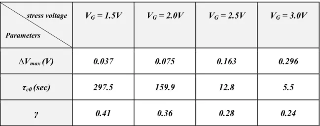
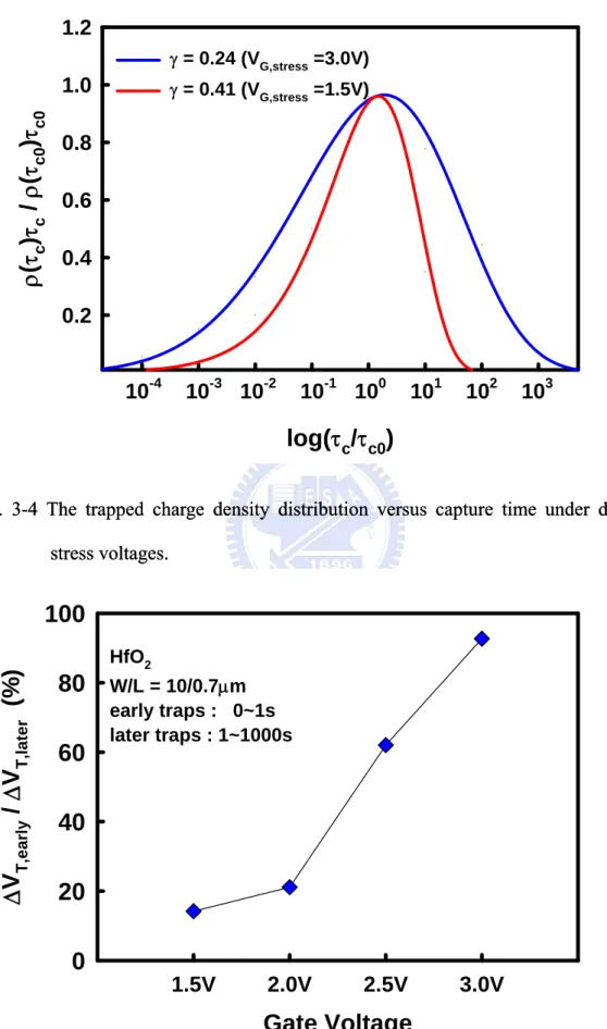
By Eq. 3.3, the three parameters (ΔVmax, γ, and τc0) that well describe the behavior of charge trapping would be obtained by fitting the symbols of Fig. 3-2. These parameters would be dependent on stress voltage with trends in Table 3-1. First, the maximum Vt shift dependent on Ntot, and xeff (q, ε, and area are fixed values) increased with increasing stress voltage. However, Ntot had been assumed a fixed value in the original of the model used in SiO2 [4]. Then, the ratio of ΔVmax of 3.0V to ΔVmax of 1.5V 8:1 would be equal to the ratio of xeff of 3.0V to xeff of 1.5V. This is inconsistent with physical principle because the maximum ratio of total thickness of the gate dielectrics to the thickness of SiON is smaller than 8:1. Thus, it could be assumed that the total density of traps (Ntot) would be a function of stress voltage and Ntot increased with increasing stress voltage. The total density of traps truly represents the maximum density of traps that can be filled by charge carriers under specific stress voltage.Next, it is inconsistent with Zafar’s previous work in the γ factor which is only dependent on high-k materials. However, the decreasing γ factor with increasing stress voltage that is consistent with our results has been reported by using power law fitting method in [5]. Therefore it is probable that the γ factor is dependent not only on high-k materials but also on stress voltage. The smaller γ factor under higher stress voltage represents the wider distribution of the capture time. According to above mentions of Ntot and γ, the trapped charge density distribution versus capture time under different stress voltages could be predicted and roughly plotted in Fig. 3-4 [6]. In the first stage of the each curve in Fig. 3-4, the increasing charge density along increasing capture time would be due to
the capture time increasing with stress time. Then, the each curve of Fig. 3-4 would reach the maximum value and become decay with capture time because the trapped electrons could build an energy barrier that induced the electrons injecting to high-k gate dielectric harder. Finally, the maximum trap density would be fully filled by electrons and the Vt shift would reach a constant. At last, the characteristic capture time constant would decrease with increasing stress voltage in Fig. 3-3due to the increasing injected charge carriers. Thus, the “early trapped” (0~1s) charge carriers would increase with increasing stress voltage demonstrated in Fig. 3-5.
The same fitting model could be used in the drain current degradation under various stress voltages in Fig. 3-6 and the trends of the parameters would be the same with the results of threshold voltage shift. Moreover, Fig. 3-7 (a) shows the threshold voltage shift as a function of stress time for HfAlO high-k gate dielectric under static stress at various gate bias voltages. Fig. 3-7 (b) shows the characteristic capture time constant under various gate bias voltages. The results showed the same trends in the three parameters with the HfO2 high-k gate dielectric and could be fitted by the same model. Comparing with the γ factor of the HfO2 gate dielectric under the same voltage, γ varies with different high-k materials and that is consistent with the Zafar’s previous work.
Fig. 3-8 shows the threshold voltage shift as a function of stress time for nMOSFETs under static stress at various temperatures. The Vt shift decreased with increasing stress temperature. The reason can be suggested that the de-trapping mechanism is dominant under higher stress temperature. Although the Vt shift seemed to slow down under higher stress temperature, the generated interface trap density measured by CP degraded more serious in Fig. 3-9. Fig. 3-10 shows the threshold voltage shift as a function of stress time for nMOSFETs under static stress at various dimensions. The Vt shift with stress time would be dependent on gate length, but independent on gate width. Moreover, the increasing gate length increased the Vt shift. The phenomenon can be
suggested that larger gate length with smaller source/drain overlap ratio induces more Vt shift because the electric field in the S/D overlap region smaller than that in the channel under the positive stress voltage.
3.4 Electron De-trapping Behavior during the Stress/Recovery Cycles
in High-k Gate Dielectric
Fig. 3-12 shows the drain current degradation for nMOSFETs under static stress/recovery time with a fixed stress voltage Vg=+2.0V and various recovery voltages Vg =+1.4~-1.4V. Under strong recovery voltage such as Vg=-1.4V, almost all the trapped electrons in the HfO2 traps could be de-trapped. As the recovery voltage was weaker, the residual electrons that couldn’t be de-trapped become more. Fig. 3-13 (a) shows the recovery region of Fig. 3-12. The symbols are measurement data and the solid lines are the fits to the results using the physical model that is built according to Zafar’s charge tapping model. The recovery model assumes that the trapped charge carriers emit with dispersive emission time constant in the pre-existing bulk traps of the high-k gate dielectrics. The operation process of the model is showed as followings:
e de MAX de de n n dt dn τ ) ( , − = (3.4) ) , ( ) ) ( exp( 1 ) exp( ) ( 1 cov , , , , 0 , , , ery re G stress G MAX de MAX de e MAX de e e MAX de e MAX de de V V n n where t n d t n n n = ⎥ ⎦ ⎤ ⎢ ⎣ ⎡ − − = ⎥ ⎥ ⎦ ⎤ ⎢ ⎢ ⎣ ⎡ ⋅ − ⋅ − =
∫
γ τ τ τ τ ρ (3.5) MAX de residue eff MAX de MAX de eff MAX T e MAX de residue de T V V V area x n q V area x n q V where t V V V V V , max , , , max 0 , max , ) ( exp Δ − Δ = Δ ⋅ ⋅ ⋅ = Δ ⋅ ⋅ ⋅ = Δ ⎥ ⎦ ⎤ ⎢ ⎣ ⎡ − ⋅ Δ + Δ = Δ − Δ = Δ ε ε τ γ (3.6)Where nde is the de-trapped charge density, ρ(τe) is the de-trapped charge density per second with continuous emission time constant, nde,MAX is the maximum density of de-trappied charge carriers as a function of recovery and stress voltage, τe/τe0 is the emission time constant/characteristic emission time constant, t is the stress time, γ is the distribution factor of ρ(τe) versus emission time constant, nT,MAX is the total density of trapped charge carriers after one thousand seconds stress under stress voltage Vg=2.0V, ε is the permittivity of the dielectric, and xeff is the centroid of trapped charge during stressing. ⎥ ⎦ ⎤ ⎢ ⎣ ⎡− ⋅ Δ + Δ ≈ Δ γ τ ) ( exp / 0 , , 0 , e MAX de residue sat d sat d t I I I I (3.7)
The drain current degradation (ΔId,sat/ Id0,sat) can be linearly transformed with the threshold voltage shift (ΔVT) from Fig. 3-11. Thus, the modeling equation can be obtained in Eq. (3.7). The four parameters (ΔIde,MAX, ΔIresidue, γ, and τe0) that can well describe the behavior of charge de-trapping are obtained by fitting the symbols of Fig. 3-13 (b). First, the sum of ΔIde,MAX and ΔIresidue under various recovery voltages would be a fixed value due to the same stress condition. ΔIde,MAX increased with the stronger recovery voltage due to the nde,MAX as a function of recovery voltage and increasing with increasing recovery voltage that would be similar to Ntot of charge trapping model. Moreover, ΔIresidue decreased with the stronger recovery voltage due to the decreasing residual trapped electrons of HfO2 gate dielectric. Next, the γ factor decreases with the stronger recovery voltage. The smaller γ factor under stronger recovery voltage represents the wider distribution of the emission time of the de-trapped charge carriers. According to above mentions of nde,MAX and γ, the de-trapped charge density distribution versus emission time under different recovery voltages could be also
predicted and roughly plotted in Fig. 3-14 which would be almost the same with Fig. 3-4 of charge trapping. At last, the characteristic emission time constant would decrease with stronger recovery voltage in Fig. 3-14. That’s because the trapped electrons with energy above the Si conduction band become more under stronger recovery voltage and the trapped electrons with energy higher than Si conduction band can emit more quickly than those with energy lower than the Si conduction band [1].
Fig. 3-15 shows the drain current degradation for nMOSFETs under static stress/recovery time with various voltages Vg=+1.5~2.5V and a fixed recovery voltage Vg =0V. Under stronger stress voltage and the same recovery voltage, the residual electrons that couldn’t be de-trapped become more. Fig. 3-16 (a) shows the recovery region of Fig. 3-15. The symbols are measurement data and the solid lines are the fits to the results using Eq. (3.7). The four parameters (ΔIde,MAX, ΔIresidue, γ, and τe0) are also obtained by fitting the symbols of Fig. 3-16 (a). First, the sum of ΔIde,MAX and ΔIresidue under the same recovery voltages would be not a fixed value due to the various stress condition. ΔIde,MAX and ΔIresidue increased with the increasing stress voltage due to the increasing trapped electrons of HfO2 gate dielectric. Thus, nde,MAX would be as a function of stress voltage and increasing with increasing stress voltage. Next, the distribution of the emission time constant is wider with increasing stress voltage due to the wider distribution of the time constant of trapped charge carriers. According to above mentions of nde,MAX and γ, the de-trapped charge density distribution versus emission time under different stress voltages could be showed in the same plot of Fig. 3-14. At last, Fig. 3-16 (b) shows the characteristic emission time constant (τe0) increasing with increasing stress voltage because of the more maximum density of de-trapped charge carriers (nde,MAX). Then, the average emission time constant of the de-trapped charge is longer after higher stress voltage
stress/recovery time with a fixed stress voltage Vg=+2.0V and various recovery voltages Vg =+0.7~-2.0V. The recovery voltage plays a significant role to clean up the trapped charge carriers before the next stress cycle. Under strong recovery voltage Vg=-2.0V, almost all the trapped electrons can be de-trapped immediately, and similar charge trapping/de-trapping behaviors can be observed during the five consecutive stress/recovery cycles. However, the charge trapping/de-trapping behaviors changed under weak recovery voltages since the trapped charge had not been completely removed at weak recovery voltages during previous recovery cycles.
3.5 Fast Electron Trapping Behavior in High-k Gate Dielectric
Fig. 3-18 shows Id-Vd curves under (a) 25℃ (b) 50℃ (c) 75℃ (d) 125℃ by two measurement methods: DC ramp and pulsed I-V. The measurement time of the conventional DC ramp measurement is about several milliseconds to seconds. The pulse width of the pulsed I-V measurement we used is 100ns and raising/falling time is 20ns. Thus, the different of Id,sat by two methods could be the charge loss with the capture time ranging from 100ns to several milliseconds. In Fig. 3-18 (a), the charge loss would be more serious with increasing gate voltage. Moreover, the charge loss would be retarded with increasing the measurement temperature because of the de-trapping mechanism dominant. These results are consistent with the results of the slow traps.
3.6 Summary
In this chapter, electron trapping and de-trapping characteristics are investigated in the pre-existing traps of the HfO2 high-k gate dielectric. During the PBTI stress, Vt shift and Id,sat degradation continue to grow and eventually become saturated, whereas the gate leakage decays with stress time and the subthreshold swing remains unchanged. According to the fitting results with the model proposed by Zafar et al., the total density of traps is not a fixed value but dependent on stress voltage and the distribution factor of capture time is dependent on not only high-k materials but also stress voltages. Moreover, the fitting results can build the distribution of the trapped charge density with capture time. The temperature effect and the geometric effect under stressing are discussed. Then, the recovery model can be built base on the charge trapping model. Our recovery model can well fit the measurement data. According to the fitting results with our model, the maximum density of de-trapped electrons is not a fixed value but dependent on stress voltage and the distribution factor of emission time is dependent on stress voltages. Moreover, the fitting results can also build the distribution of the de-trapped charge density with emission time. The fast traps can be detected by pulsed I-V measurement and the results are similar to those of slow traps.
References
[1] K. Onishi et al. “Bias-temperature instabilities of polysilicon gate HfO2 MOSFETs,” IEEE TRANSACTIONS ON ELECTRON DEVICES, VOL. 50, NO. 6, JUNE 2003.
[2] A. Kerber, E. Cartier, L. Pantisano, M. Rosmeulen, R. Degraeve, T. Kauerauf, G. Groeseneken, Senior Member, U. Schwalke, “Characterization of the Vt-instability un SiO2 HFO2 gate dielectrics,” International Reliability Physics Symposium, Dallas, Texas, 2003
[3] C. Leroux, J. Mitard, G. Ghibaudo, X. Garros, G. Reimbold, B. Guillaumot, F. Martinl, “Characterization and modeling of hysteresis phenomena in high K dielectrics,” IEDM 04-737
[4] T. H. Ning, “High-Field capture of electrons by Coulomb-attractive centers in silicon dioxide,”J. Appl. Phys. 49, 5997 (1978).
[5] Sriram Kalpat, Hsing-Huang Tseng, Michael Ramon, Mohamed Moosa, Daniel Tekleab, Philip J. Tobin, David C. Gilmer, Rama I. Hegde, C. Capasso, Clarence Tracy, and Bruce E. White, Jr., “BTI characteristics and mechanisms of metal gated HfO2 films with enhanced interface/bulk process treatments,” IEEE TRANSACTIONS ON DEVICE AND MATERIALS RELIABILITY, VOL. 5, NO. 1, MARCH 2005.
[6] A. Plonka, “Dispersive Kinetics in Condensed Phases,” Springer-Verlag, Berlin Heidelberg, (1986)
stress voltage Parameters VG = 1.5V VG = 2.0V VG = 2.5V VG = 3.0V ∆Vmax (V) 0.037 0.075 0.163 0.296 τc0 (sec) 297.5 159.9 12.8 5.5 γ 0.41 0.36 0.28 0.24
Table 3-1 The three parameters, ΔVmax, τc0, and γ, extracted by fitting under various stress voltages.
HfO2
JG = J0t-α
Stress Time (sec)
10
100
1000
J
G(A/cm
-2)
10
-610
-510
-410
-310
-210
-110
010
1 VG,stress = 1.5V α = 0.064 VG,stress = 2.0V α = 0.069 VG,stress = 2.5V α = 0.072 VG,stress = 3.0V α = 0.071 HfO2 W/L = 10/0.7μmStress Time (sec)
10
-110
010
110
210
310
4S (
m
V/decade)
70
80
90
100
110
VG,stress = 1.5V VG,stress = 2.0 V VG,stress = 2.5 V VG,stress = 3.0 VFig. 3-1 (a) the gate leakage current density and (b) the subthreshold slop as a function of stress time for nMOSFETs under static stress at various gate bias voltages.
HfO2
W/L = 10/0.7μm
Stress Time (sec)
10
-110
010
110
210
310
4Δ
V
T(m
V)
1
10
100
1000
VG = 1.5V γ=0.41 VG = 2.0V γ=0.36 VG = 2.5V γ=0.28 VG = 3.0V γ=0.24 fit curveFig. 3-2 The threshold voltage shift as a function of stress time for nMOSFETs under static stress at various gate bias voltages.
T = 25C HfO2
Stress Voltage (V)
1.4
1.6
1.8
2.0
2.2
2.4
2.6
2.8
3.0
τ
c0(s)
10
010
110
210
3log(
τ
c/
τ
c0)
ρ(
τ
c)τ
c/
ρ(
τ
c0)τ
c0 0.2 0.4 0.6 0.8 1.0 1.2 γ = 0.24 (VG,stress =3.0V) γ = 0.41 (VG,stress =1.5V) 10-4 10-3 10-2 10-1 100 101 102 103Fig. 3-4 The trapped charge density distribution versus capture time under different stress voltages.
Fig. 3-4 The trapped charge density distribution versus capture time under different stress voltages. HfO2 W/L = 10/0.7μm early traps : 0~1s later traps : 1~1000s
Gate Voltage
1.5V
2.0V
2.5V
3.0V
Δ
V
T,e a rly/
Δ
V
T,lat e r(%
)
0
20
40
60
80
100
Fig. 3-5 The ratio of early traps to fast traps under various gate bias voltages. Fig. 3-5 The ratio of early traps to fast traps under various gate bias voltages.