國 立 交 通 大 學
電子工程學系 電子研究所
博 士 論 文
積體電路電源線間具低漏電流之
靜電放電防護電路設計
LOW-LEAKAGE POWER-RAIL ESD
PROTECTION DESIGNS IN CMOS
INTEGRATED CIRCUIT
研 究 生:王 暢 資 (Chang-Tzu Wang)
指導教授:柯 明 道 (Ming-Dou Ker)
積體電路電源線間具低漏電流之
靜電放電防護電路設計
LOW-LEAKAGE POWER-RAIL ESD
PROTECTION DESIGNS IN CMOS
INTEGRATED CIRCUIT
研 究 生:王暢資
Student: Chang-Tzu Wang
指導教授:柯明道
Advisor: Ming-Dou Ker
國 立 交 通 大 學
電子工程學系 電子研究所
博 士 論 文
A Dissertation
Submitted to Department of Electronics Engineering
and Institute of Electronics
College of Electrical and Computer Engineering
National Chiao Tung University
in Partial Fulfillment of the Requirements
for the Degree of Doctor of Philosophy
in
Electronic Engineering
May 2010
Hsinchu, Taiwan, Republic of China
中華民國九十九年五月
積體電路電源線間具低漏電流之
靜電放電防護電路設計
研究生:王暢資
指導教授:柯明道 博士
國立交通大學電子工程學系電子研究所
摘要
隨著半導體製程的進步與發展,許多整合多功能的系統晶片已經成為各
電子公司的產品研發主力,奈米電子時代的來臨提供積體電路更廣泛的設
計平臺及更為前瞻的技術。許多積體電路產品已經使用奈米半導體製程技
術進行量產,但其積體電路可靠度可能會成為奈米半導體製程中更需要考
慮的問題,其中靜電放電(Electrostatic Discharge, ESD)防護已成為其中一個
重要的可靠度指標。先進的奈米半導體製程雖然能有效地微縮元件尺寸進
而提升電路運算效率,在半導體元件本身的特性卻會因尺寸過小產生許多
微米製程中不需考慮之影響,如閘極透納電流(Gate Direct Tunneling Current)
會產生嚴重的漏電而降低晶片的效能。因此在奈米製程中,全晶片靜電放
電防護設計需達到高效率、高防護能力及低漏電流之特性。另一方面,由
於晶片的操作電壓隨著製程演進持續下降以符合元件閘極氧化層可靠度及
低功率消耗之需求,但是周邊電路的電壓卻未隨半導體製程的進步而降
低,所以在扮演晶片輸入輸出媒介的混合電壓界面
(Mixed-Voltage I/O
Interface)上將會產生許多問題。因此要在此混合電壓電路加上其靜電放電
保護電路,考量界面電壓轉換及可靠度等問題,如何仔細評估這些問題而
設計出具有高的靜電放電防護能力的電路將是當今以及未來積體電路設計
上的重要課題,隨著半導體製程進入奈米級製程之後,對積體電路設計產
業更加重要。另外,隨著高壓功率積體電路製程
(Bipolar-CMOS-DMOS,
BCD)在面版驅動電路、電源供應器及電源管理等使用的普及化,對於使用
在這些應用的輸出端以及當作靜電放電保護元件的高壓電晶體來說,其高
觸發電壓及低持有電壓的特性將使得高壓積體電路的靜電放電防護能力不
足,並有可能產生閉鎖效應(Latchup)或類似閉鎖效應(Latchup-Like)的危
險。因此如何開發有效的靜電放電防護設計,將是這些高壓積體電路設計
上很重要的課題,這個主題也隨著這些產業應用上的多元化而更趨重要。
所以本論文分別針對了奈米製程應用、混合電壓界面電路以及高壓功率積
體製程應用上的限制與困難作討論,並進一步設計出有效的靜電放電防護
電路以適用在各相關應用之積體電路晶片。
為了提供適用於奈米製程,具低漏電的全晶片靜電放電防護設計,本論
文 提 出 一 新 型 靜 電 放 電 箝 制電 路 , 利 用 矽 控 整 流 器
(Silicon Controlled
Rectifier, SCR)作為靜電放電保護元件,及靜電放電偵測電路採取基體觸發
(Substrate Triggered)技術來提昇其靜電放電防護能力。矽控整流器不具有閘
極氧化層可有效避免閘極透納電流。且在考量閘極電流存在的操作情況
下,此新型靜電放電偵測電路可在正常工作時有效地降低其漏電流,此靜
電放電防護電路已在
65 奈米互補式金氧半製程中實際被製作與驗證。其人
體放電模式
(Human-Body-Model, HBM)及機器放電模式(Machine-Model,
MM)的靜電放電耐受能力可以達到 7kV 及 325V,於室溫在 1V 工作電壓
下,其漏電流僅
96nA。
為了提供有效的靜電放電防護電路於奈米製程下高低壓共容輸入輸出
電路,本論文提出可耐高工作電壓之靜電放電箝制電路,用來保護可接受
兩倍工作電壓訊號之共容輸出輸入電路。此可耐高工作電壓之靜電放電箝
制電路利用低壓薄閘極氧化層元件來實現,並納入閘極電流作為低漏電流
設計之重點。利用靜電放電匯流排及可耐高工作電壓之靜電放電箝制電路
可有效地排放各種放電組合之靜電放電電流,以保護高低壓共容輸入輸出
電路。此適用於
1V/1.8V 高低壓共容輸入輸出電路新型電路已在 65 奈米互
補式金氧半製程中實際被製作與驗證。
為了應用於高整合度之積體電路系統中,利用
N 型金氧半場效電晶體
(NMOS)阻隔的技巧之高低壓共容輸入輸出電路被設計用來接受三倍、四倍
甚至五倍的操作電壓,本論文提出兩個利用低電壓元件所實現的可耐受三
倍工作電壓之靜電放電防護設計,透過不同的設計概念達到基體觸發之效
用,提供有效的觸發電流,以提升防護元件之靜電放電耐受能力。本論文
所提出應用在
1.2V/3.3V 高低壓共容輸出入界面之靜電放電防護設計已經
在
130 奈米 1.2V 互補式金氧半製程下實現並已在 3.3V 的操作環境下驗證。
在高壓功率積體電路製程技術中,擴散式金氧半電晶體(DMOS)被廣泛
地使用於靜電放電防護元件。本論文以擴散式金氧半電晶體為基礎提出新
型的靜電放電防護電路以提升防護元件之導通效能及靜電放電耐受度。在
正常電路操作時,擴散式金氧半電晶體可偏壓於
40V 而其 5V 閘極氧化層
不會受到可靠度問題,另一方面此電路可進一步設計以避免高壓積體電路
發生閉鎖效應或類似閉鎖效應的危險。此電路已在
0.35 微米 5-V/40-V 高壓
功率積體電路製程中實際被製作與驗證。
本論文分別針對了奈米金氧半導體製程特性、混合電壓界面電路以及高
壓功率積體電路製程應用上的限制與困難作討論,並設計出低漏電、高效
能、並且在正常工作時不會受到閉鎖效應危險的靜電放電防護電路,所設
計的靜電放電防護電路均已在實際晶片上成功驗證,並有相對應的國際期
刊論文發表與專利申請。
LOW-LEAKAGE POWER-RAIL ESD PROTECTION
DESIGNS IN CMOS INTEGRATED CIRCUITS
Student: Chang-Tzu Wang Advisor: Dr. Ming-Dou Ker
Department of Electronics Engineering and Institute of Electronics
National Chiao Tung University
Abstract
Continually scaling down the CMOS technologies into nanoscale generation imposes significant challenges in integrated circuit (IC) reliability, where electrostatic discharge (ESD) protection has become one of the major concerns. To meet such reliability specifications are necessary for IC product qualification. From the perspective of ESD, the similar gate oxide breakdown voltage and trigger voltage of MOSFET devices increased the design difficulty. Moreover, the secondary device characteristics of MOSFET have been considered in nanoscale CMOS generations. The most important impact for ESD is the gate direct tunneling current, which happens between the gate and silicon beneath the gate oxide, occurs while MOSFET implementing in a nanoscale CMOS process. Such gate tunneling current could induce a substantial fraction of overall leakage current in a chip. The traditional ESD protection circuit with a large gate oxide dimension suffers serious gate leakage issue. The on-chip ESD protection circuit in nanoscale CMOS process should be design with consideration of gate tunneling current to achieve a low standby leakage current during the normal circuit operation condition. During the ESD stress, the on-chip ESD protection circuit should provide efficient protection capability to assure the safety of the internal circuit which has a small gate oxide breakdown voltage in nanoscale CMOS process. For the mixed-voltage I/O interfaces with thin gate-oxide devices, the on-chip ESD protection
designs will meet design difficulties, such as gate-oxide reliability constraints and undesired leakage current paths. In high-voltage Bipolar-CMOS-DMOS (BCD) technology, high-voltage transistors have been widely used for display driver ICs, power supplies, and power management ICs. The high-trigger-voltage and low-holding-voltage characteristics of HV transistor have been found to cause latchup or latchup-like failure and insufficient ESD efficiency. Therefore, how to develop an efficient on-chip ESD protection design is an important challenge for high-voltage IC products. In this dissertation, the ESD design constraints in nanoscale CMOS process, mixed-voltage I/O interfaces, and high-voltage CDMOS technology are presented. Furthermore, the novel design solutions for on-chip ESD protection circuit have been developed to meet the design constraints in such technologies and applications.
To provide effective on-chip ESD protection with low standby leakage current in nanoscale CMOS technology, a new power-rail ESD clamp circuit by using the silicon controlled rectifier (SCR) device and ESD detection circuit with substrate-triggered technique is proposed. The SCR device without poly-gate structure has good immunity against the gate leakage current. The special ESD detection circuit is designed with consideration of gate current to reduce the standby leakage current. The new proposed design has been fabricated and verified in a 65nm fully-silicided CMOS process. The new proposed power-rail ESD clamp circuit can achieve 7kV in human-body-model (HBM) and 325V in machine-model (MM) ESD levels while consuming only a standby leakage current of 96nA at room temperature under 1-V bias.
In order to protect the mixed-voltage I/O interfaces in nanoscale CMOS technology, a new high-voltage-tolerant ESD clamp circuit is proposed to protect the mixed-voltage I/O circuits for receiving signals with 2×VDD voltage level. The devices used in the high-voltage-tolerant ESD protection design are all low-voltage thin gate-oxide devices. The gate current of each thin gate devices in the high-voltage-tolerant ESD detection circuit has also been considered. By using the ESD protection scheme with the ESD bus and the proposed high-voltage-tolerant ESD clamp circuit, the mixed-voltage I/O circuit can be well protected. The new proposed circuit has been fabricated in a 1-V 65-nm CMOS process for experimental verification.
In high integrated electronic system, the mixed-voltage I/O design with NMOS blocking technique is applied for receiving 3×VDD, 4×VDD, and even 5×VDD input signals without
the gate-oxide reliability issue. In this dissertation, two new ESD protection design by using only 1×VDD low-voltage devices for mixed-voltage I/O buffer with 3×VDD input tolerance are proposed. Two different special high-voltage-tolerant ESD detection circuits are designed with substrate-triggered technique to improve ESD protection efficiency of ESD clamp device. These two ESD detection circuits with different design concepts both have effective driving capability to trigger the ESD clamp device on. These ESD protection designs have been successfully verified in two different 130nm 1.2-V CMOS processes to provide excellent on-chip ESD protection for 1.2-V/3.3-V mixed-voltage I/O buffers.
In high voltage CDMOS technology, the high-voltage DMOS is widely used as on-chip ESD protection devices. The trigger voltage of the high-voltage devices is too high to protect the output buffer. Such characteristics will cause the high-voltage DMOS susceptible to the latchup or ESD danger in the practical applications. To greatly improve ESD performance of the high-voltage DMOS devices, gate-driven and substrate-triggered circuit techniques are applied. The proposed gate-driven and substrate-triggered ESD protection circuits have been successfully verified in a 0.35-μm 5V/40V bipolar CMOS DMOS (BCD) process. In addition, the power-rail ESD protection design can be also achieved with stacked structure to protect 40-V power pins without latchup issue in the smart power ICs.
In this dissertation, the novel ESD protection circuits have been developed for nanoscale CMOS process, mixed-voltage I/O interfaces and high-voltage BCD process with high ESD robustness. Each of the ESD protection circuits has been successfully verified in the testchips. The proposed ESD protection circuits in this dissertation can achieve the benefits of low standby leakage current, high ESD performance, and latchup-free characteristics for whole chip ESD design in CMOS ICs.
Acknowledgment
在交通大學電子研究所的生涯中,首先要感謝我的指導教授柯明道教
授,從大學部的專題研究到碩士班和博士班,在這一路上提供我最好的學
習資源及研究環境,並耐心的指導與鼓勵,使我能順利完成博士學業。除
了在半導體專業領域上的訓練,柯教授認真的研究態度與嚴謹的處事原
則,讓我學會在有限的時間內,有效率地處理事務、正確地解決問題、並
交出高水準的成果。
感謝交通大學吳重雨校長、中山大學王朝欽教授、晶焱科技姜信欽博
士、國研院晶片中心邱進峰博士、工業技術研究院吳文慶博士、交通大學
陳明哲教授與李義明教授在百忙之中抽空擔任我的口試委員,並給予珍貴
的指導與建議,讓此博士論文更加完整。
在這段求學的過程中,『聯華電子股份有限公司』的『可靠度技術發展
處』給予我研究上的支持與協助,從實驗晶片的下線及量測設備的支援協
助,使得我實驗研究能夠順利完成。在此特別要感謝蘇冠丞處長、唐天浩
資深經理所給予的支持與鼓勵,使本論文的研究成果得以成功驗證,並順
利發表於國際期刊與國際研討會。
感謝
307 實驗室的前輩徐國鈞博士、陳世倫博士、許勝福博士、陳榮昇
博士、張瑋仁博士、蕭淵文博士、陳世宏博士、顏承正博士、林群祐博士、
羅文裕、徐新智、李健銘、陳志豪、陳穩義、吳偉琳、賴泰翔、陳佳惠、
王資閔、李宇軒、陳世範、溫詠儒、邱柏硯、陸亭州、蔡惠雯等諸位學長
姊、同學與學弟們在研究與生活上的協助與扶持。此外,感謝實驗室助理
卓慧貞小姐在行政事務上的許多協助。
另外我還要感謝交大男子排球隊的張振興教練以及所有隊友們,讓我在
研究的過程中能適當的紓解壓力,得以再度面對更多的研究難題。
由衷感謝敬愛的父母親王互先生及吳廷妹女士、哥哥王暢湘、弟弟王暢
君。有了您們的支持、鼓勵、陪伴和照顧,才能讓我順利完成學業。還要
謝謝女友高筱雯小姐,一路上陪伴著我。感謝所有幫助我、陪伴我一同成
長的師長、朋友、學長姊、同學、學弟妹們,願大家平安喜樂。
王
暢
資
謹誌於竹 塹 交 大
九十九年 五月
Contents
Abstract (Chinese)
i
Abstract (English)
iv
Acknowledgment
vii
Contents viii
Table Captions
xii
Figure Captions
xiv
1 Introduction 1
1.1 Gate Direct Tunneling Current in Nanoscale CMOS 1
1.1.1 Gate Current in N/P-Type MOSFET Devices 1
1.1.2 Modeling of Gate Direct Tunneling Current 2
1.2 Background of ESD Protection 5
1.2.1 Issue of Mixed-Voltage I/O Interface 8
1.2.2 Issue of High Voltage BCD ICs 12
1.3 ESD Protection Design for Mixed-Voltage I/O Interface 13
1.3.1 Stacked-NMOS Device with Substrate-Triggered Technique 13 1.3.2 Additional ESD Protection Circuit between I/O pad and Power Pad 13
1.3.3 ESD Protection Design with ESD Bus 14
1.4 Organization of This Dissertation 14
2 Low Leakage ESD Protection Design for Nanoscale CMOS
Process
17
2.1 Background 17
2.1.1 Influence of Gate Current on ESD Protection Circuit 18
2.1.2 Gate Current through MOS Capacitor 19
2.2 ESD Protection Design with Consideration of Gate Current 20 2.2.1 Traditional RC-based ESD Clamp Circuit with Gate Current 20
Consideration
2.2.2 Modified ESD Clamp Circuit with Gate Current Consideration 22
2.3 Ultra Low-Leakage Power-Rail ESD Clamp Circuit 23
2.3.1 Design Procedure 24
2.3.2 Operation under Normal Circuit Operating Condition 26
2.3.3 Operation under ESD Transient Even 27
2.4 Experimental Results 28
2.4.1 Turn-on Verification 29
2.4.2 ESD Robustness 30
2.4.3 Standby Leakage and Design Flexibility 33
2.4.4 Discussion 35
2.5 Summary 36
3 Low Leakage ESD Protection Design for 2
×VDD Mixed-Voltage
I/O Circuits
39
3.1 Background 39 3.2 Review on High-Voltage-Tolerant ESD Power-Rail ESD Clamp Circuit
with Consideration of Gate Current
41 3.3 Low-Leakage 2×VDD-Tolerant Power-Rail ESD Clamp Circuit 42
3.3.1 Design Procedure 44
3.3.2 Operation under Normal Circuit Operating Condition 46
3.3.3 Operation under ESD Transient Event 47
3.4 Experimental Results 48
3.4.1 Standby Leakage Current 50
3.4.2 Turn-on Verification 52
3.4.3 ESD Robustness 53
3.4.4 Failure Analysis 55
3.4.5 Discussion 57
3.5 Summary 57
4 3
×VDD-Tolerant Power-Rail ESD Clamp Circuit
59
4.2 ESD Protection Scheme for 3×VDD-Tolerant Mixed-Voltage I/O Buffer 60
4.3 3×VDD-Tolerant ESD Clamp Circuit A 63
4.3.1 Operation under Normal Circuit Operating Condition 64
4.3.2 Operation under ESD Transition 65
4.4 3×VDD-Tolerant ESD Clamp Circuit B 67
4.4.1 Operation under Normal Circuit Operating Condition 67
4.4.2 Operation under ESD Transition 68
4.5 Discussion on 3×VDD-Tolerant ESD Clamp Circuits 71
4.6 Experimental Results 71
4.6.1 DC I-V Characteristics of ESD Clamp Device 72
4.6.2 Turn-on Verification 73
4.6.3 TLP Characteristics and ESD Robustness of ESD Protection Design With 3×VDD-Tolerant ESD Clamp Circuit A
75
4.6.4 TLP Characteristics and ESD Robustness of ESD Protection Design With 3×VDD-Tolerant ESD Clamp Circuit B
75
4.7 Pin-to-Pin ESD Protection 77
4.8 Summary 78
5 ESD Protection Design for 5-V/40-V High-Voltage BCD
Technology
81
5.1 Background 81 5.2 Characteristics of LDNMOS with Gate-Biased and
Substrate-Triggered Effect
83
5.2.1 LDNMOS with Gate-Biased Technique 85
5.2.2 LDNMOS with Substrate-Triggered Technique 88
5.3 Implementation of ESD Protection Circuit with LDNMOS 89
5.4 Experimental Results 90
5.4.1 TLP Characteristics of Stand-Alone LDNMOS with Gate-Biased or Substrate-Triggered Effects
91
5.4.2 ESD Performance of LDNMOS with Gate-Coupled Design 93 5.4.3 ESD Performance of LDNMOS with Gate-Driven and
Substrate-Triggered ESD Detection Circuits
5.4.4 Failure Analysis 95
5.5 Power-Rail ESD Protection Design 95
5.6 Summary 97
6 Conclusions and Future Works
99
6.1 Main Results of This Dissertation 99
6.2 Future Works 101
References 103
Vita 113
Table Captions
Chapter 2
Table 2.1. Oxide Thickness and Gate Current of Gate-Oxide of N/P MOSFET under
1-V Bias in Different CMOS Technologies 19
Table 2.2. Dimensions of Devices in the ESD detection Circuit of the Modified ESD
Clamp Circuit with Timer Level Restorer for HSPICE Simulation 23 Table 2.3. Dimensions of Devices in the ESD detection Circuit of The Proposed
Power-Rail ESD Clamp Circuit 26
Table 2.4. ESD Robustness of the Proposed Power-Rail ESD Clamp Circuit with
SCR Device of Different Widths 32
Table 2.5. Comparison among the Proposed Power-Rail ESD Clamp Circuit and
Prior Works 36
Chapter 3
Table 3.1. Dimensions of Devices in the ESD Detection Circuit of the Nnew
Proposed 2×VDD-Tolerant Power-Rail ESD Clamp Circuit 46 Table 3.2. Dimensions of devices in the ESD detection circuit of the previous
2×VDD-Tolerant Power-Rail ESD Clamp Circuit (Fig. 3.3) 50 Table 3.3. ESD Robustness of the Proposed Power-Rail ESD Clamp Circuit with
SCR Device of Different Widths 55
Table 3.4. Comparison between the Proposed Power-Rail ESD Clamp Circuit and
Prior work 57
Chapter 4
Table 4.1. ESD Robustness of I/O Buffer with or without ESD Protection Circuit
with ESD Clamp Circuit A 75
Table 4.2. ESD Robustness of the Proposed ESD Protection Circuit with ESD Clamp
Chapter 5
Table 5.1. Comparison of ESD Robustness among the Gate-Coupled LDNMOS, Gate-Driven ESD Protection Circuit, and Substrate-Triggered ESD
Figure Captions
Chapter 1
Fig. 1.1. Illustration of gate direct tunneling components of a very short-channel
NMOSFET. (Igs and Igd are EDT currents). 3
Fig. 1.2. Gate bias dependent band diagrams and electron tunneling in the channel (Igc ) and the gate edge (Igs and Igd ). (a) Vg > 0 V (inversion mode). (b)
Vfb < Vg < 0 V (depletion mode). 5
Fig. 1.3. The four pin-combination modes for ESD test on an IC product: (a) positive-to-VSS (PS-mode), (b) negative-to-VSS (NS-mode), (c)
positive-to-VDD (PD-mode), and (d) negative-to-VDD (ND-mode). 6 Fig. 1.4. VDD-to-VSS ESD tests: (a) positive mode, and (b) negative mode. 7 Fig. 1.5. Typical on-chip ESD protection scheme with power-rail ESD clamp
circuit in a CMOS IC. 7
Fig. 1.6. Typical circuit diagrams for the traditional CMOS I/O buffer. The leakage current and the gate-oxide reliability appear while I/O pad receives
2×VDD input signals. 9
Fig. 1.7. Typical circuit diagrams for the mixed-voltage I/O circuits with the
stacked NMOS and the N-well self-biased PMOS. 9
Fig. 1.8. The ESD current paths of (a) the traditional I/O pad with power-rail ESD clamp circuit, and (b) the mixed-voltage I/O pad with power-rail ESD clamp circuit, under the positive-to-VSS (PS-mode) ESD stress. The ESD
current paths are indicated by the dashed lines. 11
Chapter 2
Fig. 2.1. The traditional RC-based power-rail ESD clamp circuit. 18 Fig. 2.2. The modified power-rail ESD clamp circuit with timer level restorer. 19 Fig. 2.3. The gate current of the MOS capacitor in different CMOS technologies. 20 Fig. 2.4. HSPICE-simulated voltage on the nodes of the ESD detection circuit and
the gate current flow through the MOS capacitor Mc in the traditional RC-based power-rail ESD clamp circuit under the normal power-on
Fig. 2.5. The proposed ultra-low-leakage power-rail ESD clamp circuit with p-type substrate-triggered SCR device as ESD clamp device, where the ESD
detection circuit is designed with consideration of gate leakage current. 24 Fig. 2.6. HSPICE-simulated voltage on the nodes of the ESD detection circuit and
the gate current flow through the MOS capacitor Mc1 in the proposed ultra-low leakage ESD clamp circuit in a 65-nm CMOS process under the
normal power-on condition. 27
Fig. 2.7. HSPICE-simulated voltages on the nodes of the ESD detection circuit and the substrate-triggered current which flows into the SCR device under
0-to-5V ESD-like transition on VDD. 28
Fig. 2.8. Layout view of the proposed power-rail ESD clamp circuit. 28 Fig. 2.9. Chip photograph of the test patterns of the proposed power-rail ESD
clamp circuit. The chip has been fabricated in a 65-nm CMOS process
with 1-V devices. 29
Fig. 2.10. The measured voltage waveforms clamped by the proposed ESD clamp
circuit by applying a 0-to-5V voltage pulse to VDD pad. 30 Fig. 2.11. The TLP-measured I-V characteristics of the proposed power-rail ESD
clamp circuit with SCR device of different widths under positive-to-VSS ESD stress. The TLP-measured I-V curve of the stand-alone SCR device
without ESD detection circuit is also included in this figure. 31 Fig. 2.12. The TLP-measured I-V characteristics of the proposed power-rail ESD
clamp circuit with SCR device of 45μm under different TLP rise times of
10ns, 2ns, and 200ps. 32
Fig. 2.13. The dependence of TLP-measured It2 and MM ESD levels on SCR device
of different widths. 33
Fig. 2.14. The dependence of the standby leakage current under 1-V bias of the
whole ESD clamp circuit at different temperatures. 34 Fig. 2.15. The TLP-measured trigger voltage of the SCR device, on the device size
Chapter 3
Fig. 3.1. ESD protection schemes for mixed-voltage I/O interface with
2×VDD-tolerant ESD clamp circuit, where the power supply is powered
by voltage level of 2×VDD. 40
Fig. 3.2. ESD protection schemes for mixed-voltage I/O interface with ESD bus and 2×VDD-tolerant ESD clamp circuit, where the power supply is
powered by voltage level of VDD. 40
Fig. 3.3. The prior work of the 2×VDD-tolerant power-rail ESD clamp circuit used
to protect the mixed-voltage I/O buffers [77]. 42
Fig. 3.4. The proposed low-leakage 2×VDD-tolerant power-rail ESD clamp circuit with p-type substrate-triggered SCR device as ESD clamp device, where the ESD detection circuit is designed with consideration of gate leakage
current. 44 Fig. 3.5. HSPICE-simulated voltage on the nodes of the ESD detection circuit in a
65-nm CMOS process under the normal power-on condition with VDD_H
of 1.8V and VDD of 1V. 47
Fig. 3.6. HSPICE-simulated voltages on the nodes of the ESD detection circuit and the substrate-triggered current which flows into the SCR device under
0-to-5V ESD-like transition on VDD_H. 48
Fig. 3.7. Layout view of the proposed 2×VDD-tolerant power-rail ESD clamp circuit. The chip has been fabricated in a 65-nm CMOS process with 1-V
devices. 49 Fig. 3.8. The standby leakage current of the proposed ESD clamp circuit and the
prior work of ESD detection circuit with and without STNMOS in Fig. 2
at (a) 25oC and (b) 125 oC. 51
Fig. 3.9. The measured voltage waveforms clamped by the proposed
2×VDD-tolerant ESD clamp circuit by applying a 0-to-5V voltage pulse to VDD_H of the proposed ESD clamp circuit with VSS grounded and VDD
Fig. 3.10. The TLP-measured I-V characteristics of the proposed power-rail ESD clamp circuit with SCR device of different widths under positive
VDD_H-to-VSS ESD stress. The TLP pulse used in this measurement is with pulse width of 100ns and rise time of ~2ns. The inset figure showed the room-in view on the snapback holding point, where the holding
voltage is ~2V. 54
Fig. 3.11. The TLP-measured I-V curve of the stacked NMOS in the mixed-voltage I/O buffer. The trigger voltage of the stacked NMOS in the mixed-voltage
I/O buffer is around 6V. 54
Fig. 3.12. (a) After 6.75kV VDD_H-to-VSS HBM ESD stress, the electrical
abnormal region of the ESD clamp circuit was located at the SCR device. (b) The failure spots were found at the anode-to-cathode path of the SCR
device. 56
Chapter 4
Fig. 4.1. The proposed ESD protection scheme for mixed-voltage I/O buffer with
3×VDD input tolerance realized with only 1×VDD devices. 60 Fig. 4.2. Device structure of the ESD clamp device composed of substrate-
triggered SCR device with diodes in series. 63
Fig. 4.3. Circuit implementation of the 3×VDD-tolerant ESD clamp circuit A
realized with 1×VDD devices. 64
Fig. 4.4. Cross-sectional view of the NMOS Mn1 and the HSPICE-simulated voltages at the nodes of ESD detection circuit under the normal circuit
operating condition. 65
Fig. 4.5. HSPICE-simulated voltages on the nodes of ESD detection circuit and the substrate-triggered current through Mp5 under 0-to-6V ESD-like transition
on ESD bus. 66
Fig. 4.6. Circuit implementation of the 3×VDD-tolerant ESD clamp circuit B
realized with 1×VDD devices. 67
Fig. 4.7. HSPICE-simulated voltages on the nodes of the proposed ESD detection
Fig. 4.8. HSPICE-simulated voltages on nodes of the ESD detection circuit under normal circuit operating conditions with 10% voltage variation in the ESD
bus line. 70
Fig. 4.9. HSPICE-simulated voltages on the nodes of ESD detection circuit under 0-to-6V ESD-like transition on ESD bus line (the line for node e overlaps
with the line for node u). 70
Fig. 4.10. The measured dc I-V characteristics of the ESD clamp device (SCR with 2
diodes in series) under different temperatures. 72 Fig. 4.11. The measured dc I-V characteristics of the ESD clamp device (SCR with 2
diodes in series) under different substrate-triggered currents (I_trig). 73 Fig. 4.12. The measured voltage waveforms, clamped by 3×VDD-tolerant ESD
clamp circuit A and B, on the I/O pad when a 0-to-6V voltage pulse is applying to I/O pad under the PS-mode ESD stress (VDD floating and
VSS grounded). 74
Fig. 4.13. The measured TLP I-V characteristics of the ESD clamp device in the 3×VDD-tolerant ESD clamp circuit B with or without ESD detection
circuit under PS-mode ESD stress. 76
Fig. 4.14. The shared ESD bus and 3×VDD-tolerant ESD clamp circuit for whole set
of I/O buffers to achieve pin-to-pin ESD protection. 78
Chapter 5
Fig. 5.1. ESD protection design for applications of (a) output pad of LED driver and (b) DC-DC converter. The resistor RESD in advanced CMOS process is
not allowed in such applications. 82
Fig. 5.2. (a) The device cross-sectional view, and (b) the layout top view, of the octagonal unit cell of the n-channel LDMOS with 5-V gate oxide and 40-V drain-to-source operating voltage in a 0.35-µm 5V/40V BCD
process. 83 Fig. 5.3. After 3kV HBM ESD stress, the failure spot were found at only a few
contacts at the drain side of the LDNMOS drawn with multiple finger
Fig. 5.4. The layout top view of a LDNMOS which is constructed by 2 × 2 octagonal cells. In this structure, the P_Body regions of all the cells are
connected to each other. 85
Fig. 5.5. The TCAD simulated I-V curves (IDS-VDS) of the LDNMOS device with
different gate biases. 86
Fig. 5.6. (a) The TCAD simulated I-V curves of the LDNMOS device, and the corresponding electric field distribution of the LDNMOS device with (b)
Vg of 0V and (c) Vg of 5V under VDS of 10V and VDS of 47V. 87 Fig. 5.7. (a) The TCAD simulated I-V curves of the LDNMOS device with
different substrate-triggered currents (I_trig), and (b) the electric field
distribution at VDS of 10V and VDS of 45V under I_trig of 1mA/μm. 88 Fig. 5.8. The proposed ESD protection circuits with (a) gate-driven, and (b)
substrate-triggered, ESD detection circuits. 90
Fig. 5.9. TLP-measured I–V curves of the LDNMOS device drawn by 2 × 2 octagonal cells with device width of 320μm under different gate-biased
voltages (Vg). 92
Fig. 5.10. TLP-measured I–V curves of the LDNMOS device by with 2 × 2 octagonal cells with device width of 320μm under different
substrate-triggered currents (I_trig). 92
Fig. 5.11. The TLP-measured I-V characteristics of the gate-coupled LDNMOS (drawn by multiple-finger structure with width of 300μm) with resistors of
10kΩ and 50kΩ connected from gate to source. 93
Fig. 5.12. The TLP-measured I-V characteristics of the LDNMOS with the proposed
ESD detection circuits and the gate-coupled LDNMOS. 94 Fig. 5.13. After 4.6-kV HBM ESD stress, the failure spots were found at the drain
contacts of each unit cell of the LDNMOS device with the gate-driven
ESD protection circuit. 96
Fig. 5.14. (a) The latchup-free ESD protection circuit realized with four
stacked-LDNMOS devices and the gate-driven ESD detection circuit for 40-V power pins, and (b) the corresponding TLP-measured I-V
Chapter 1
Introduction
In this chapter, the background of this dissertation is discussed. First, the gate direct tunneling current in nanoscale fully-silicided complementary metal-oxide-semiconductor (CMOS) processes are discussed. Then, the issue of electrostatic discharge (ESD) protection and mixed-voltage I/O interface realized in low-voltage CMOS process are introduced. Finally, the rest of this dissertation is organized.
1.1 Gate Direct Tunneling Current in Nanoscale CMOS
Improvement in circuit performance of operating frequency and density of the CMOS integrated circuits (IC) for aggressive device scaling with gate lengths down into nanoscale regime. Aggressive scaling of CMOS technology has reduced the SiO2 gate dielectric
thickness below 3nm. Major causes for concern in further reduction of oxide thickness include increased poly-silicon gate depletion, boron penetration into the channel region, and high direct tunneling gate leakage current which leads to questions regarding dielectric integrity, reliability, and standby power consumption. According to the International Technological Roadmap for Semiconductors (ITRS), gate oxide thicknesses of 1.2–1.5 nm have been required in 2004 for sub-100-nm CMOS. For such an ultrathin gate oxide, direct tunneling current will dominate the gate leakage current and the off-state power dissipation of the transistor [1]-[2]. For the transistors in conventional CMOS process, the dominant leakage mechanism is mainly due to short channel effects owing to drain-induced barrier lowering (DIBL). However, in the ultrathin gate oxide transistors, the gate leakage current could contribute to standby leakage current significantly, which may result in faulty circuit operation since designers may assume that there is no appreciable gate current.
1.1.1 Gate Current in N/P-Type MOSFET Devices
The gate current arises due to the finite probability of an electron directly tunneling through the insulating SiO2 layer. The amount of the gate current is a strong exponential
function of the gate oxide thickness as well as the voltage potential across the gate oxide. A difference in gate oxide thickness of 0.2nm can result in an order of magnitude change in the gate current, making it the most sensitive parameter with respect to any physical dimensions. Even the gate oxides can be well controlled (within ±4% in general), as compared to other device dimensions (such as effective channel length or width of metal line), this significant sensitivity makes serious variation in the gate current among different dies in the same wafer. Another key point is that the gate current of a PMOS device is typically one order of magnitude smaller than that of an NMOS device, under the identical gate oxide thickness and voltage potential across the gate oxide[3]-[4]. This is due to the much higher energy required for hole tunneling in SiO2 and the fact that there are very few electrons associated with a
PMOS device. However, in alternate dielectric materials the energy required for electron and hole tunneling can be completely different. In the case of nitrided gate oxides, in use today in some processes, the gate current of the PMOS can actually exceed that of the NMOS depending on the nitrogen concentration (higher nitrogen content increases the gate current of the PMOS relative to the NMOS) [5]-[6].
1.1.2 Modeling of Gate Direct Tunneling Current
Direct tunneling of the conduction band electron from inversion or accumulation layers has been extensively studied [7]-[9]. As for p+ polysilicon gate p-MOSFETs, direct tunneling hole was found to dominate the gate current under channel inversion conditions [10]-[11]. The direct tunneling current appearing between the source–drain extension (SDE) and the gate overlap, so-called the edge direct tunneling (EDT), dominates off-state drive current, especially in very short channel devices [12], [13].
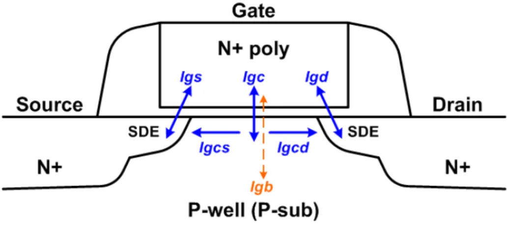
Gate direct tunneling current is produced by the quantum-mechanical wave function of a charged carrier through the gate oxide potential barrier into the gate, which depends not only on the device structure but also bias conditions. The various gate tunneling components in a scaled NMOSFET are illustrated in Fig. 1.1. The gate-to-channel current (Igc), the gate-to-bulk current (Igb), and the EDT currents (Igs and Igd) are shown. In long-channel devices, Igs and Igd are less important than Igc because the gate overlap length is small compared to the channel length. In very short channel devices, the portion of the gate overlap compared to the total gate length becomes larger.
Fig. 1.1 Illustration of gate direct tunneling components of a very short-channel NMOSFET. (Igs and Igd are EDT currents)
Fig. 1.2 illustrates the band diagrams and electron tunneling directions along the gate-to-channel and gate-to-SDE directions for a highly doped drain (HDD) NMOSFET. For Vg > 0V, the gate-to-channel tunneling current (Igc) is the dominant current component, since a higher gate oxide voltage (Vox) appears between the gate and the channel, as shown in
Fig. 1.2(a). Here, the Vfb of an NMOSFET with an n-type polysilicon gate (i.e., n+ poly/SiO2
/p-substrate) is approximately -1V, while the Vfb along the gate-to-SDE (i.e., n+ poly/SiO2
/n+ SDE) is approximately 0 V. On the contrary, the EDT currents (Igs and Igd) can become dominant for bias conditions of Vfb < Vg < 0V. For the gate-to-SDE case, electrons
accumulated in the n+ poly gate tunnel to the SDE region can lead to an appreciable off-state current. Meanwhile, operating in the depletion mode along the n+ poly/SiO2/p-substrate surface, few electrons are present in the channel that can in turn tunnel into the gate, as shown in Fig. 1.2(b). Such gate currents in ultrathin oxide transistors have been modeled in BSIM4 MOSFET model [14].
In BSIM4 model, the oxide voltage Vox is written as
Vox =Voxacc+Voxdepinv, (1.1) Voxacc =Vfbzb +VFBeff , (1.2) Voxdepinv =K1ox Φs +Vgsteff, (1.3) where Voxacc and Voxdepinv are the oxide voltages in accumulation and in inversion (depletion),
respectively. The components of gate tunneling current include the tunneling current between gate and bulk (Igb), the current between gate and channel (Igc), and the current between gate
and source/drain diffusion regions (Igs and Igd). The gate-to-bulk current is partitioned into two components for the MOSFET in accumulation (Igbacc) and in inversion (Igbinv). Igbacc and Igbinv are given by
[
( ) (1 )]
exp _ oxacc oxacc Igbacc aux gb oxRatio eff eff V CIGBACC V BIGBACC AIGBACC TOXE B V V T A L W Igbacc ⋅ + ⋅ ⋅ − ⋅ − ⋅ ⋅ ⋅ ⋅ ⋅ = , and (1.4)[
( ) (1 )]
exp _ oxdepinv oxdepinv Igbinv aux gb oxRatio eff eff V CIGBINV V BIGBINV AIGBINV TOXE B V V T A L W Igbinv ⋅ + ⋅ ⋅ − ⋅ − ⋅ ⋅ ⋅ ⋅ ⋅ = . (1.5)The current between gate-to-source/drain diffusion regions are given by
⎥⎦ ⎤ ⎢⎣ ⎡− ⋅ ⋅ − ⋅ ′ ⋅ + ⋅ ′ ⋅ ′ ⋅ ⋅ ⋅ ⋅ = ) 1 ( ) ( exp gs gs gs gs e oxRatioEdg eff V CIGSD V BIGSD AIGSD POXEDGE TOXE B V V T A DLCIG W Igs , and (1.6) ⎥⎦ ⎤ ⎢⎣ ⎡− ⋅ ⋅ − ⋅ ′ ⋅ + ⋅ ′ ⋅ ′ ⋅ ⋅ ⋅ ⋅ = ) 1 ( ) ( exp gd gd gd gd e oxRatioEdg eff V CIGSD V BIGSD AIGSD POXEDGE TOXE B V V T A DLCIG W Igd . (1.7)
The gate-to-channel current is formulated as
[
( ) (1 )]
exp _ oxdepinv oxdepinv Igc aux gse oxRatio eff eff V CIGC V BIGC AIGC TOXE B V V T A L W Igc ⋅ + ⋅ ⋅ − ⋅ − ⋅ ⋅ ⋅ ⋅ ⋅ = . (1.8) With consideration of drain bias effect, Igc has been partitioned into two parts as Igcs and Igcd, which are expressed as4 2 2 4 10 2 10 1 1 ) exp( 0 − − × + ⋅ × + − ⋅ − + ⋅ ⋅ = dseff dseff dseff V PIGCD V PIGCD V PIGCD Igc Igcs , and (1.9) 4 2 2 4 10 2 10 1 ) exp( ) 1 ( 1 0 − − × + ⋅ × + ⋅ − ⋅ + ⋅ − ⋅ = dseff dseff dseff V PIGCD V PIGCD V PIGCD Igc Igcd , (1.10)
where Igc0 equals Igc at Vds of 0V.
From equations (1.4)-(1.8), the main parameters of a MOSFET that dominate the gate current include the effective channel width, channel length, and the voltage difference between the gate and the other terminals.
(a) Vg > 0 V
(b) Vfb < Vg < 0 V
Fig. 1.2 Gate bias dependent band diagrams and electron tunneling in the channel (Igc ) and the gate edge (Igs and Igd ). (a) Vg > 0 V (inversion mode). (b) Vfb < Vg < 0 V (depletion mode).
1.2 Background of ESD Protection
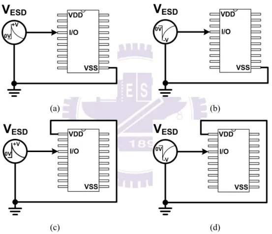
ESD failure has become the main reliability concern on semiconductor products, especially for the system-on-a-chip (SOC) implementation in nanoscale CMOS processes. Common ESD failures are destructive, leading to immediate malfunction of ICs caused by either thermal breakdown in silicon and/or metal interconnects due to high-current transient or dielectric breakdown in gate oxide due to high-voltage overstress [15]. To sustain reasonable ESD robustness in nanoscale CMOS IC’s, on-chip ESD protection circuits must be added into the chips. ESD specification of commercial IC products are required to be higher than 2kV in human-body-model (HBM) and 200V in machine-model (MM) ESD stress [16], [17]. According to the SESD standards, the ESD stress can be applied to any pin with another pin grounded in an IC. Therefore, on-chip ESD protection circuits have to be
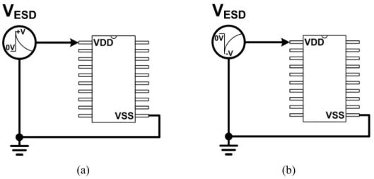
designed and placed around the input, output, and power pads to provide efficient ESD protection in CMOS ICs against unexpected ESD damages in the internal circuits of CMOS ICs [18]–[24]. ESD stresses on an I/O pad have four pin-combination modes: positive-to-VSS (PS-mode), negative-to-VSS (NS-mode), positive-to-VDD (PD-mode), and negative-to-VDD (ND-mode), as shown in Figs. 1.3(a) ~ 1.3(d), respectively. For comprehensive ESD verification, the positive and negative VDD-to-VSS ESD stresses had also been specified to verify the whole-chip ESD robustness, which are shown in Figs. 1.4(a) and 1.4(b).
(a) (b)
(c) (d)
Fig. 1.3. The four pin-combination modes for ESD test on an IC product: (a) positive-to-VSS (PS-mode), (b) negative-to-VSS (NS-mode), (c) positive-to-VDD (PD-mode), and (d) negative-to-VDD (ND-mode).
(a) (b) Fig. 1.4. VDD-to-VSS ESD tests: (a) positive mode, and (b) negative mode.
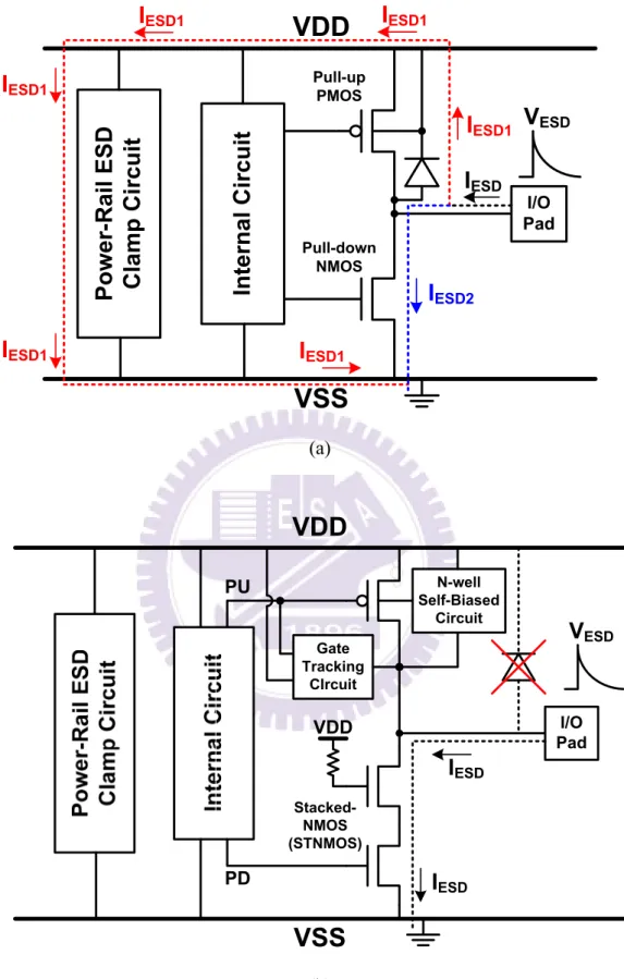
The typical design of on-chip ESD protection configuration, with efficient power-rail ESD clamp circuit between VDD and VSS power lines, in a CMOS IC is illustrated in Fig. 1.5 [24]. Such ESD protection scheme can be designed to meet the requirements for circuit operation of general purpose I/O while providing ESD immunity to the necessary ESD levels. The power-rail ESD clamp circuit is implemented by ESD clamp device (MESD) and a
RC-based ESD detection circuit. The clamp device (MESD) can either operate in snapback or
can be sized to conduct the ESD current through the channel. The elements R and C can be shared by numerous power-rail ESD clamp circuits in the whole-chip ESD protection design..
1.2.1 Issue of Mixed-Voltage I/O Interface
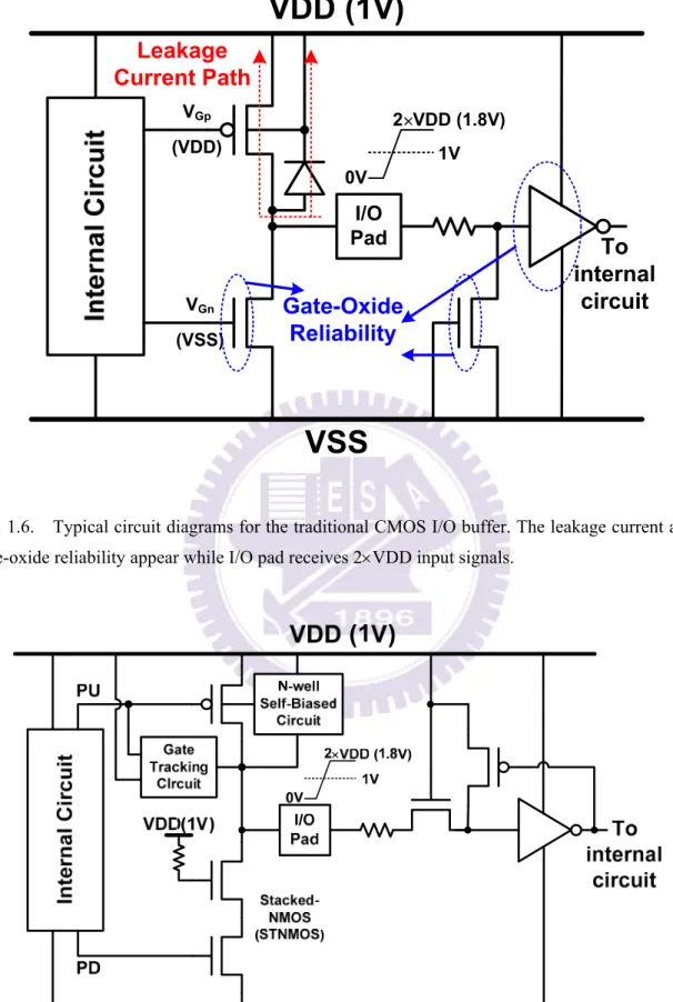
With the scaled-down device dimension in advanced CMOS technology, the power supply voltage is also scaled down to reduce the power consumption and to meet the gate-oxide reliability. Therefore, chip design quickly migrates to the lower voltage level with the advancement of the nanoscale CMOS technology. However, some peripheral components or other ICs in a microelectronic system are still operated at the higher voltage levels. In other words, an electronic system could have chips operated at different voltage levels. From the perspective of circuit design for whole system integration, the I/O buffers may drive or receive high-voltage signals to communicate with other ICs. Thus, some circuits must be design in low-voltage process, but still operated in the high-voltage or mixed-voltage (high-voltage and low-voltage) environments. Several problems arise in the I/O interface between these ICs, such as the gate-oxide breakdown [25]-[27] and the undesirable leakage current paths [28]. Fig. 1.6 shows the input and output stage of the traditional CMOS I/O buffer with VDD of 1V and 1-V gate oxide MOSFETs. When an external 1.8-V signal is applied to the I/O pad, the conducted channel of the pull-up PMOS and the parasitic drain-to-well junction diode in the pull-up PMOS will cause the leakage current paths from I/O pad to VDD, as the dashed lines shown in Fig. 1.6. Besides, the 1-V gate oxides of the pull-down NMOS in the output stage and the inverter in the input stage will be over-stressed by the 1.8-V input signal and then suffer the gate-oxide reliability problem.
To solve the gate-oxide reliability issue without using the additional thick gate-oxide process (called dual gate oxide in some CMOS processes), the stacked-NMOS configuration had been widely used in the mixed-voltage I/O buffer to reduce the process complexity and fabrication cost of the chip [29]–[35]. The typical 2×VDD-tolerant mixed-voltage I/O circuit (e.g. 1V/1.8V mixed-voltage I/O interface) is shown in Fig. 1.7. The gate of top NMOS in the stacked-NMOS device is biased at VDD (e.g. 1V in a 1V/1.8V mixed-voltage I/O interface), and the gate of bottom NMOS is biased by the pre-driver circuit. The independent control on the top and bottom gates of stacked-NMOS device allows the devices to meet reliability limitations during normal circuit operation with an input signals with 2×VDD voltage level (e.g. 1.8V in a 1V/1.8V mixed-voltage I/O interface). The gate tracking circuits and the N-well self-biased circuits are designed to ensure that the pull-up PMOS, between the I/O pad and the VDD power line, does not conduct current when the 1.8-V input signals enter the I/O pad. In such mixed-voltage I/O circuits, the on-chip ESD protection circuits will meet more design constraints and difficulty.
VGp (VDD) I/O Pad 0V 2 VDD (1.8V)
To
internal
circuit
VGn (VSS)Leakage
Current Path
Gate-Oxide
Reliability
1VFig. 1.6. Typical circuit diagrams for the traditional CMOS I/O buffer. The leakage current and the gate-oxide reliability appear while I/O pad receives 2×VDD input signals.
Fig. 1.7. Typical circuit diagrams for the mixed-voltage I/O circuits with the stacked NMOS and the N-well self-biased PMOS.
The ESD protection design of I/O pad cooperating with power-rail ESD clamp circuit for traditional I/O circuit and 2×VDD-tolerant mixed-voltage I/O circuit are shown in Fig. 1.8(a) and 1.8(b), where a PS-mode ESD pulse is applied to the I/O pad. In the traditional I/O circuit, the PS-mode ESD pulse can be discharged via two effective paths, as shown in Fig. 1.8(a). The one is through the NMOS in the output buffer by snapback breakdown. The other is through the parasitic diode of PMOS from I/O pad to VDD and power-rail ESD clamp circuit to VSS grounded. However, due to the leakage current issue in the mixed-voltage I/O circuits, there is no diode connected from the I/O pad to VDD power line in the mixed-voltage I/O circuits, as shown in Fig. 1.8(b). Without such diode connected from the I/O pad to VDD in the mixed-voltage I/O circuits, the ESD current at I/O pad under PS-mode ESD stress cannot be discharged from the I/O pad to VDD power line, and cannot be discharged through the additional VDD-to-VSS ESD clamp circuit. Therefore, the power-rail ESD clamp circuit did not help to pull up ESD level of the mixed-voltage I/O pad under the PS-mode ESD stress. In this situation, the ESD current at the I/O pad is mainly discharged through the stacked-NMOS by snapback breakdown. Besides, comparing the single NMOS and the stacked-NMOS in the high-current snapback region, the stacked-NMOS will have a higher trigger voltage, a higher snapback holding voltage, slower turn-on speed, and a lower secondary breakdown current. Therefore, such mixed-voltage I/O circuits with stacked-NMOS often have much lower ESD level under the PS-mode ESD stress, as compared to the traditional I/O circuits with a single NMOS [36], [37]. In addition, without the diode connected from the I/O pad to VDD, the mixed-voltage I/O circuit also has a lower ESD level for I/O pad under PD-mode ESD stress. The absence of the diode between I/O pad and VDD power line in the mixed-voltage I/O circuits will seriously degrade ESD performance of the I/O pad under the PS-mode and PD-mode ESD stresses. By using extra process modification such as ESD implantation, the ESD robustness of stacked-NMOS device can be further improved [38], [39], but the process complexity and fabrication cost are increased. In addition, the induced high voltage on the gate of top NMOS transistor under ESD stress will cause high-current crowding effect in the channel region to seriously degrade ESD robustness of stacked-NMOS device in the mixed-voltage I/O circuits [40]. Therefore, effective ESD protection design without increasing process complexity is strongly requested by the mixed-voltage I/O circuits in the scaled-down CMOS processes.
VSS
Internal Circuit
VDD
I/O Pad Pull-down NMOSV
ESDPower-Rail ESD
Clamp Circuit
Pull-up PMOS
I
ESD1I
ESDI
ESD1I
ESD1I
ESD1I
ESD1I
ESD1I
ESD2 (a) VDDVSS
VDD
Stacked-NMOS (STNMOS) N-well Self-Biased Circuit Gate Tracking CIrcuit PU PD I/O PadVESD
IESD
IESD
(b)Fig. 1.8. The ESD current paths of (a) the traditional I/O pad with power-rail ESD clamp circuit, and (b) the mixed-voltage I/O pad with power-rail ESD clamp circuit, under the positive-to-VSS (PS-mode) ESD stress. The ESD current paths are indicated by the dashed lines.
1.2.2 Issue of High Voltage BCD ICs
High-voltage Bipolar-CMOS-DMOS (BCD) technology has been widely used in LCD driver circuits, telecommunication, power switch, motor control systems, etc [41]. In the smart-power technology, bipolar junction transistor, high-voltage CMOS, high-voltage lateral DMOS, and silicon controlled rectifier (SCR) device were used as on-chip ESD protection devices [42]–[50]. Some ESD protection designs used the lateral or vertical bipolar transistors as ESD protection devices in smart power technology [48]. However, fabrication cost and process complexity are increased by adding vertical bipolar modules into a high-voltage BCD process without epitaxial layer. With a thick gate oxide of several hundred angstroms, the high-voltage CMOS device, which can sustain high-voltage, was often used as the ESD protection device because it can work as both of output driver and ESD protection device simultaneously in the high-voltage ICs. With an ultra-high operating voltage, the ESD robustness of high-voltage CMOS device is quite weaker than that of low-voltage MOSFET. Moreover, the high-voltage lateral DMOS device with a thin gate oxide to gain the small turn-on resistance and driving capability was usually implemented with several hundred thousand micrometers as the large-sized output buffer in some applications, such as DC-DC converters, and class-D amplifier. In this case, an additional efficient ESD protection device should be placed in parallel with the output buffer. Besides, such ESD protection device must be designed with not only a robust ESD capability but also the fast turn-on speed in case the output buffer was damaged before the ESD protection device turned on. To increase ESD robustness, the conventional design with large device dimension still suffers the non-uniform current distribution among the device. The high-voltage NMOS has the extremely strong snapback phenomenon during ESD stress, which often results in non-uniform turn-on variation among the multi-fingers of high-voltage NMOS [51]. Moreover, the holding voltage of the high-voltage devices in snapback breakdown condition has been found to be much smaller than the power supply voltage. Such characteristics will cause the high-voltage ICs susceptible to the latchup or latchup-like danger in the practical system applications, especially while these devices are used in the power-rail ESD clamp circuit. To overcome the problem of non-uniform turn-on phenomenon, the gate-coupling technique was applied to the HV NMOS [45], [52]. However, the gate of HV NMOS must be in series with a large resistor, which occupies a large layout area. Hence, how to improve the ESD robustness of the high-voltage NMOS with a reasonable silicon area is indeed an important reliability issue in
the high-voltage BCD technology. In this dissertation, the gate-driven and substrate-triggered ESD protection designs realized with the high-voltage lateral DMOS with consideration of latchup issue is proposed.
1.3 ESD Protection Design for Mixed-Voltage I/O Interface
1.3.1 Stacked-NMOS Device with Substrate-Triggered Technique
To improve the turn-on uniformity among the multiple fingers of CMOS output buffer, the substrate-triggered designs [53]-[56] have been reported to increase ESD robustness of the large-device-dimension nMOS. The substrate-triggered circuit for providing the trigger current should be designed to avoid electrical overstress on the gate oxide and to prevent the undesired leakage current paths during normal circuit operating condition. During ESD stress condition, the substrate-triggered circuit should generate large enough current to effectively improve the turn-on efficiency of parasitic n-p-n BJT in stacked NMOS device. The substrate-triggered circuit should meet above constraints for providing effective ESD protection to the mixed-voltage I/O interfaces. By using this substrate-triggered design, the gates of stacked NMOS in the mixed-voltage I/O circuits can be fully controlled by the pre-driver of I/O circuits without conflict to the ESD protection circuits. Therefore, the ESD robustness of mixed-voltage I/O circuits can be effectively improved without occupying extra silicon area to realize the additional stand-alone ESD protection device into the I/O cells.
1.3.2 Additional ESD Protection Circuit between I/O pad and Power Pad
To improve ESD level of the mixed-voltage I/O circuits, the additional ESD protection circuit was added between I/O pad and VSS power pad [57], [58]. Under the PS-mode ESD stress, the ESD current at the I/O pad is designed to be directly discharged through such additional ESD protection circuit to the grounded VSS. Under the PD-mode ESD stress, the ESD current at the I/O pad can be discharged through the additional ESD protection circuit to VSS power line, and then through the parasitic diode of power-rail ESD clamp circuit to the grounded VDD. The substrate-triggered lateral n-p-n BJT device [57] and the stacked NMOS triggered SCR (SNTSCR) [56], have been verified to protect the mixed-voltage I/O circuits. On the other hand, the additional ESD protection circuit can also be added between I/O pad and VDD power pad to improve the ESD robustness [59]-[61]. Under the PD-mode ESDstress, the ESD current at the I/O pad is designed to be directly discharged through such additional ESD protection circuit to the grounded VDD. Under the PS-mode ESD stress, the ESD current at the I/O pad can be discharged through the additional ESD protection circuit to VDD power line, and then through the power-rail ESD clamp circuit to the grounded VSS. The diode string, which can sustain high ESD current in forward-biased condition, has been used for protecting the mixed-voltage I/O circuits [59], [60]. The number of diodes in the diode string is determined by the voltage difference between the maximum input voltage at the I/O pad and the VDD supply voltage. The area of such diodes must be scaled up by the number of the diodes to keep the low turn-on resistance from I/O pad to VDD during the ESD stress event. The additional ESD protection device connected between I/O pad the VDD pad can also be implemented by the gate p-n-p BJT, which has been verified to protect the mixed-voltage I/O circuits [59]. In this design, the gated p-n-p BJT can effectively clamp the overstress ESD pulse during the ESD stress event, and meet the gate-oxide reliability constraints without leakage current path during the normal operation.
1.3.3 ESD Protection Design with ESD Bus
The whole-chip ESD protection scheme with the additional ESD bus for the 2×VDD-tolerant and 3×VDD-tolerant mixed-voltage I/O interfaces are proposed in Chapter 3 and Chapter 4 in this dissertation. The additional ESD bus line is realized by a wide metal line in CMOS IC [62]. The ESD bus is not directly connected to an external power pin, but biased via a diode to VDD. The diode connected between the VDD power line and ESD bus is also used to block the leakage current path from the I/O pad to VDD during normal circuit operating condition with a high-voltage input signal. The ESD protection scheme with ESD bus and the circuit operation are discussed in detail in Chapter 3 in this dissertation. With the turn-on-efficient power-rail ESD clamp circuits, high ESD level for the mixed-voltage I/O circuits can be achieved by this ESD protection scheme with ESD bus.
1.4 Organization of This Dissertation
To overcome the ESD design constraints in nanoscale CMOS process, mixed-voltage I/O interfaces and high-voltage BCD process, the novel ESD protection circuits have been developed and verified in this dissertation. This dissertation contains six chapters. Chapter 1 presents an introduction of the gate direct tunneling current in the thin gate-oxide MOS transistor while implemented in nanoscale CMOS technology and an overview on the design
concept and circuit implementations of the ESD protection designs for mixed-voltage I/O interfaces without using the additional thick gate-oxide process. To improve ESD level of the mixed-voltage I/O circuits, the ESD protection design without increasing the process complexity is strongly requested by the mixed-voltage I/O circuits in consumer IC products. Such ESD protection design in the mixed-voltage I/O circuits still meets the gate-oxide reliability constraints, and needs to prevent the undesired leakage current paths during normal circuit operating condition. Under ESD stress condition, the ESD protection circuit should be quickly triggered on to discharge ESD current.
In chapter 2, a new power-rail ESD clamp circuit with low standby leakage current for nanoscale IC product is proposed. The low-leakage power-rail ESD clamp circuit is composed of substrate-triggered SCR device and special ESD detection circuit. The traditional RC-based ESD protection design with consideration of gate current issue is discussed. Compared with the traditional large-sized MOSFET as ESD clamp device, the SCR device without poly-gate structure has good immunity against the gate leakage current. The special ESD detection circuit is designed with consideration of gate current to reduce the standby leakage current. By controlling the gate current of the devices in the ESD detection circuit under a specified bias condition, the whole power-rail ESD clamp circuit can achieve a low standby leakage current. Without using additional low-leakage or thick gate-oxide devices (which need extra mask layers and process flows), the new proposed design has been fabricated and verified in a 1-V 65nm fully-silicided standard CMOS process.
In chapter 3, a new high-voltage-tolerant ESD clamp circuit is proposed to protect the mixed-voltage I/O circuits for receiving signals with 2×VDD voltage level. The devices used in the high-voltage-tolerant ESD protection design are all 1V low-voltage thin gate-oxide NMOS/PMOS devices which can be safely operated under the 1.8V bias conditions without suffering from the gate-oxide reliability issue. The gate current of each thin gate devices in the high-voltage-tolerant ESD detection circuit has also been considered. By using the ESD protection scheme with the ESD bus and the proposed high-voltage-tolerant ESD clamp circuit, the mixed-voltage I/O circuit can be well protected. The four mode (PS, NS, PD, and ND) ESD stresses on the mixed-voltage I/O circuits can be effectively discharged. The new proposed circuit has been fabricated in a 1-V 65-nm standard CMOS process for experimental verification.
In chapter 4, two new ESD protection design by using only 1×VDD low-voltage devices for mixed-voltage I/O buffer with 3×VDD input tolerance are proposed. Two different special
high-voltage-tolerant ESD detection circuits are designed with substrate-triggered technique to improve ESD protection efficiency of ESD clamp device. These two ESD detection circuits with different design concepts both have effective driving capability to trigger the ESD clamp device on. These ESD protection designs have been successfully verified in two different 130nm 1.2-V standard CMOS processes to provide excellent on-chip ESD protection for 1.2-V/3.3-V mixed-voltage I/O buffers.
In chapter 5, the ESD protection design for smart power applications with lateral double-diffused MOS (LDMOS) transistor is investigated. With the gate-driven and substrate-triggered circuit techniques, the n-channel LDMOS can be quickly turned on to protect the output drivers during ESD stress event. From the experimental results, the high-voltage lateral DMOS with the proposed ESD detection circuit has better TLP-measured It2, ESD robustness, and turn-on efficiency than the stand-alone lateral DMOS. The proposed gate-driven and substrate-triggered ESD protection circuits have been successfully verified in a 0.35-μm 5V/40V bipolar CMOS DMOS (BCD) process.
Finally, the main results of this dissertation are summarized in chapter 6. Some suggestions for the future works are also addressed in this chapter.
Chapter 2
Low Leakage ESD Protection Design for Nanoscale
CMOS Process
In this chapter, a new power-rail ESD clamp circuit with low standby leakage current for nanoscale IC product is proposed. The low-leakage power-rail ESD clamp circuit is composed of substrate-triggered SCR device and ESD detection circuit. The SCR device without poly-gate structure has good immunity against the gate leakage current. The new proposed ESD clamp circuit has an efficient ESD detection circuit to improve the turn-on efficiency of the ESD clamping device. By using the new proposed circuit solution with only thin gate-oxide devices, the standby leakage current of the proposed power-rail ESD clamp circuit can be successfully reduced under the normal circuit operating condition. The proposed power-rail ESD clamp circuit has been successfully verified in a 1-V 65-nm CMOS process. [63].
2.1 Background
With the decrease of the power supply voltage for low power applications, the thickness of the gate oxide has been also scaled down in the nanometer CMOS technologies. However, such a thin gate oxide of only ~2nm in advanced CMOS technology has been reported to result in a substantial fraction of the overall leakage current in the chip due to its gate leakage current [64]. In 45-nm generation and beyond, the metal gate technology is therefore applied to reduce the gate leakage current [65]. Nevertheless, the gate leakage issue still exists in the 90-nm and 65-nm CMOS technologies which are currently used in production without the high-k metal gate structure. The gate current has been modeled in BSIM4 MOSFET model, and the foundries have also provided the corresponding SPICE models of nanometer CMOS processes to circuit designers. Recently, some work has been reported on how to reduce the gate leakage current for digital circuits in advanced CMOS processes [66]-[68].
2.1.1 Influence of Gate Current on ESD Protection Circuit
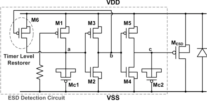
From the perspective on commercial IC products, to achieve the electrostatic discharge (ESD) specification is necessary for product qualification. The power-rail ESD clamp circuit to effectively protect the core circuits is traditionally implemented by RC-based ESD protection structure with a large-sized ESD clamping MOSFET [chap1]. Such a traditional RC-based ESD clamp circuit is shown in Fig. 2.1. However, the gate leakage current caused from the large-sized MOSFET (MESD) and the MOS capacitor (Mc) in the traditional
power-rail ESD clamp circuit becomes serious in nanoscale CMOS processes. Such gate current through the MOS capacitor could influence the function of the traditional ESD protection circuit seriously. With such a leakage current in the MOS capacitor, the ESD clamping MOSFET (MESD) cannot be completely turned off under the power-on condition
due to the malfunction of the ESD detection circuit caused by gate leakage current and in turn to induce extra large leakage current through MESD. Such a leaky ESD protection circuit is
barely tolerable in portable products with low power requirements. To solve the problem of malfunction in the traditional RC-based ESD detection circuit, the modified ESD clamp circuit with the timer level restorer was ever reported as that re-drawn in Fig. 2.2 [69]. But, the experimental result in that work still showed a high standby leakage current in the order of several micro-amperes in a 130-nm CMOS process at a high temperature of 125°C [69]. New designs of the power-rail ESD clamp circuit need to be developed to further reduce such standby leakage current in nanometer CMOS processes.
Fig. 2.2. The modified power-rail ESD clamp circuit with timer level restorer.
2.1.2 Gate Current through MOS Capacitor
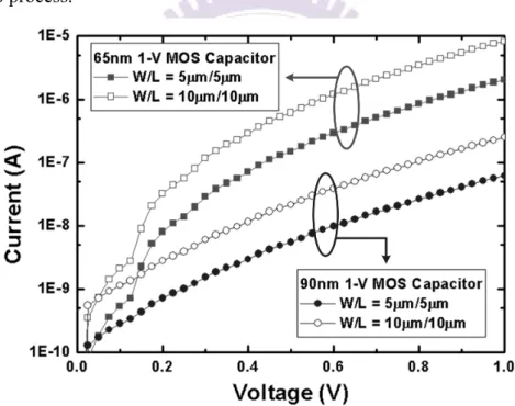
The gate leakage current cannot be neglected when the gate oxide thickness is scaled down to 3nm and below. The oxide thickness and the total gate current across the gate-oxide of N/P MOSFET with W/L of 1μm/1μm under 1-V bias in 90-nm, 65-nm, and 45-nm CMOS processes are compared in Table 2.1. In BSIM4 model [14], the components of gate tunneling current include the tunneling current between gate and bulk (Igb), the current between gate and channel (Igc), and the current between gate and source/drain diffusion regions (Igs and Igd).
Table 2.1
Oxide Thickness and Gate Current of Gate-Oxide of N/P MOSFET under 1-V Bias in Different CMOS Technologies
For a MOS capacitor, the source, drain, and bulk terminals are connected to the same node. Therefore the total gate-to-source current (Igcs+Igs), the total gate-to-drain current (Igcd+Igd), and the gate-to-bulk current (Igb) of a MOS capacitor with W/L of 5μm/5μm can be simulated with foundry provided SPICE parameters. The corresponding currents are 1.02μA, 1.02μA, and 89pA, respectively, in a 65-nm CMOS process under 1-V bias. Compared with gate-to-source current and gate-to-drain current, the component of gate-to-bulk current in a MOS capacitor is quite small in comparison to the simulated results. The simulated total gate current of the MOS capacitor with W/L of 5μm/5μm and 10μm/10μm in 65-nm and 90-nm CMOS processes are shown in Fig. 2.3. From Fig. 2.3, the gate current of a MOS capacitor is directly dependent on the area of the poly gate structure. Besides, the gate leakage problem in 65-nm CMOS process is more serious than that in 90-nm CMOS process.
Fig. 2.3. The gate current of the MOS capacitor in different CMOS technologies.