國 立 交 通 大 學
電子工程學系 電子研究所
博 士 論 文
互補式金氧半積體電路靜電放電防護之設計最佳
化與故障分析
Design Optimization and Failure Analysis of
On-Chip ESD Protection in CMOS Integrated
Circuits
研 究 生:陳 世 宏 (Shih-Hung Chen)
指導教授:柯 明 道 (Ming-Dou Ker)
互補式金氧半積體電路靜電放電防護之設計最佳
化與故障分析
Design Optimization and Failure Analysis of
On-Chip ESD Protection in CMOS Integrated
Circuits
研 究 生:陳世宏
Student: Shih-Hung Chen
指導教授:柯明道
Advisor: Ming-Dou Ker
國 立 交 通 大 學
電子工程學系 電子研究所
博 士 論 文
A Dissertation
Submitted to Department of Electronics Engineering
and Institute of Electronics
College of Electrical and Computer Engineering
National Chiao Tung University
in Partial Fulfillment of the Requirements
for the Degree of Doctor of Philosophy
in
Electronic Engineering
January 2009
Hsinchu, Taiwan, Republic of China
i
-互補式金氧半積體電路靜電放電防護之設計最
佳化與故障分析
研究生:陳世宏
指導教授:柯明道 博士
國立交通大學電子工程學系電子研究所
摘要
隨著奈米尺度互補式金氧半製程時代的來臨與系統單晶片應用的持續發展,靜電放 電(Electrostatic Discharge, ESD)防護已成為積體電路產品可靠度中相當艱鉅的挑戰。為 避免積體電路遭受靜電放電的威脅與破壞,所有積體電路與外界接觸的輸入輸出銲墊 (Pad)或是電源銲墊,皆須搭配靜電放電防護設計。然而,輸入輸出銲墊上的靜電放電 防護電路會在訊號路徑上產生寄生效應。若訊號路徑上的寄生效應過大,將導致電路性 能的嚴重衰減。尤其於類比輸入輸出界面電路與跨電源組之內部傳輸界面電路應用中, 靜電放電防護電路在訊號路徑上引起的寄生效應必須達到最小化的設計。寄生效應嚴格 限制的情況下,電源箝制靜電放電防護電路(Power-Rail ESD Clamp Circuit)是達成積體 電路產品全晶片靜電放電防護極為有效的設計。它不僅可以提升電源線至接地線的靜電 放電防護能力,亦能顯著強化輸入輸出銲墊至電源線(VDD)與接地線(VSS)或是接點對 接點(Pin-to-Pin)的靜電放電防護能力。搭配電源箝制靜電放電防護電路與類比輸入輸出 銲墊的靜電放電防護電路,將可共構出適用於類比輸入輸出界面電路的低寄生效應靜電 放電防護電路。此外,跨電源組內部傳輸界面電路的靜電放電防護問題,亦可利用電源 箝制靜電放電防護電路與主動式跨電 源組靜電放電防護電路(Active Cross-Power- Domain ESD Protection Circuit)成功獲得解決。具備有效且可靠的靜電放電防護設計,能 夠提供奈米尺度積體電路產品足夠的耐用年限,並能讓產品使用者更加安心。ii
-制靜電放電防護電路,已經廣泛使用於奈米尺度互補式金氧半製程技術的積體電路產 品 。 這 些 電 源 箝 制 靜 電 放 電 防 護 電 路 具 有 一 特 定 電 路 架 構 , 即 是 以 多 級 反 相 器 (Multi-Stage Inverters)實現控制電路,驅動主靜電放電箝制 N 型金氧半電晶體(Main ESD Clamp NMOS Transistor)。本論文的第二章分析兩種控制電路架構,分別為三級反相器 與一級反相器,對於靜電放電防護與應用所造成的影響,藉以驗證適用於電源箝制靜電 放電防護電路的最佳化設計。研究中發現不良的電路設計架構,會導致 N 型金氧半電 晶體的電源箝制靜電放電防護電路,在電性高速暫態(Electrical Fast Transient, EFT)測試 與高速電源啟動(Fast Power-On)測試下,發生異常的閂鎖導通現象(Latch-On Event)。本 章後段利用高敏度微光顯微鏡(Emission Microscope, EMMI),清楚解釋電源箝制靜電放 電防護電路的異常閂鎖導通故障機制。
除了控制電路以外,N 型金氧半電晶體電源箝制靜電放電防護電路的靜電放電暫態 偵測電路(ESD-Transient Detection Circuit)亦是決定電源箝制靜電放電防護電路性能與 應用的關鍵因素。本論文第三章提出了一個嶄新的靜電放電暫態偵測電路,其特點為極 小的靜電放電暫態偵測電容設計下,成功延長主靜電放電箝制 N 型金氧半電晶體導通 時間,進而提升電源箝制靜電放電防護電路的導通效率與靜電放電耐受度。此外,這個 靜電放電暫態偵測電路擁有優異抵抗誤觸發(Mis-Trigger)與閂鎖導通的能力,可以安全 使用於高速電源啟動的特殊電路系統。
在電源箝制靜電放電防護電路的設計中,主靜電放電箝制元件(Main ESD Clamp Device)將是直接影響靜電放電防護能力的最主要因素。一直以來,矽控整流器元件 (Silicon Controlled Rectifier, SCR)即是以極高的單位面積靜電放電耐受度而備受矚目。 然而過高的觸發電壓與較差的導通速度,使得矽控整流器元件在先進製程的靜電放電防 護應用上受到很大的限制。本論文的第四章提出具有低觸發電壓與高導通效率的常開型 效能矽控整流器設計(Initial-On SCR Design)。未使用特殊的常開型元件與未進行製程調 整的情況下,以矽控整流器元件搭配內嵌 P 型金氧半電晶體做為觸發控制電路完成常開 型效能矽控整流器設計,適用於一般的互補式金氧半製程技術,大大增加矽控整流器元 件於深次微米與奈米尺度積體電路的靜電放電防護應用。此外,這個常開型效能的矽控 整流器於 2.5 伏特的操作電壓下擁有足夠高的導通電壓(Holding Voltage, Vh),可避免電 性閂鎖(Latchup)的問題。經由實驗晶片量測結果,以 P 型金氧半電晶體觸發的常開型效 能矽控整流器,已成功驗證於 0.25 微米互補式金氧半製程技術。 本論文第五章針對前一章所提出的金氧半電晶體觸發矽控整流器(MOS-Triggered
iii
-SCR)元件進行設計最佳化的分析與研究。金氧半電晶體觸發矽控整流器元件的觸發機 制與靜電放電電流分佈會受到內嵌金氧半電晶體的通道長度的改變而有所不同,通道 長度將對於矽控整流器元件的觸發電壓(Trigger Voltage, Vt1)、導通電壓、導通電阻(On Resistance, Ron)、二次崩潰電流(Second Breakdown Current, It2)與靜電放電耐受度有相 當大的影響。為使金氧半電晶體觸發矽控整流器於深次微米與奈米尺度的積體電路之 靜電放電防護應用中達到最佳效能,內嵌金氧半電晶體的通道長度與電路佈局設計最 佳化已透過各項參數的分析比較呈現於第五章。 於類比輸入輸出界面電路的應用中,本論文第六章以兩種類比輸入輸出銲墊的靜電 放電防護電路,搭配不同的電源箝制靜電放電防護電路進行設計最佳化研究。本章使用 0.18 微米 1.8 伏特與 3.3 伏特互補式金氧半製程技術,分別設計了四種可應用於類比輸 入輸出界面電路的靜電放電防護電路。其中,分析三種電源箝制靜電放電箝制元件分別 為 閘 極 驅 動 N 型 金 氧 半 電 晶 體 (Gate-Driven NMOS) 、 基 體 觸 發 的 場 氧 化 層 元 件 (Substrate-Triggered Field-Oxide Device, STFOD) 與 基 體 觸 發 N 型 金 氧 半 電 晶 體 (Substrate-Triggered NMOS, STNMOS),在類比輸入輸出界面電路的電源箝制靜電放電 防護電路中的防護效能,藉以找出適當的電源箝制靜電放電箝制元件。經由實驗晶片量 測結果,在 0.18 微米的互補式金氧半製程技術中,適用於類比輸入輸出界面電路的靜 電放電防護設計,是以雙二極體(Double Diode)作為類比輸入輸出銲墊上的靜電放電防 護電路,這兩個二極體分別放置於類比輸入輸出銲墊至電源線與接地線間,搭配閘極驅 動 N 型金氧半電晶體電源箝制靜電放電防護電路。經由掃瞄式電子顯微鏡的觀察,四 種類比輸入輸出電放電防護設計的故障機制,獲得更完整的分析與討論。施加負靜電放 電 電 壓 於 類 比 輸 入 輸 出 銲 墊 且 電 源 線 接 地 的 測 試 條 件 (Negative-to-VDD Mode, ND-Mode)下,以雙二極體與基體觸發場氧化層元件所建構的類比輸入輸出靜電放電防 護設計,產生了異常的故障點。這個故障機制是由於寄生於靜電放電防護二極體與 N 型防護環(Guard Ring)間的 npn 雙極性接面電晶體(Bipolar Junction Transistor, BJT)意外 觸發導致大量靜電放電電流,經這個寄生 npn 雙極性接面電晶體釋放造成防護環的燒熔 破壞。本章的最後針對此故障機制提出相對應的解決方案。 由於積體電路設計的複雜化,越來越多的電路功能整合入同一個單晶片上,而這些 電路區塊因為操作電壓的不同與電源雜訊耦合的考量,各自擁有獨立的電源組,然而這 樣的獨立電源組架構相當不利於跨電源組靜電放電防護,使得跨電源組靜電放電防護設 計成為極需被解決的問題。本論文第七章首先探討了一件積體電路產品的跨電源組界面
iv -電路故障案例。於此案例中,產品的人體放電模式靜電放電耐受度可以達到 2000 伏特, 但其機械放電模式靜電放電耐受度則無法達到 150 伏特。施加負靜電放電電壓於輸入輸 出銲墊且電源線接地的機械放電模式的測試條件下,靜電放電電流經由跨電源組界面電 路釋放,造成界面電路的閘極氧化層、接面與接觸(Contact)的嚴重燒熔破壞。藉由故障 分析技術,清楚分析跨電源組靜電放電電流釋放路徑與故障機制。本章的第二部分,針 對目前已發表的跨電源組界面電路靜電放電防護設計進行分析,藉以更進一步了解跨電 源組間靜電放電防護設計策略。在本章的最後一部份,提出了適用於跨電源組界面電路 的主動式跨電源組靜電放電防護設計,並且於 130 奈米互補式金氧半製程技術中獲得成 功的驗證。於跨電源組人體放電模式與機械放電模式靜電放電測試中,其靜電放電耐受 度分別達到 4000 伏特與 400 伏特。 第八章總結本論文的研究成果,並提出數個接續本論文研究方向的研究題目。本論 文所提出的各項新型設計,均搭配實驗晶片量測結果以驗證設計之理論,且有相對應的 國際期刊與國際研討會論文發表。本論文中數個創新設計已提出專利申請。
DESIGN OPTIMIZATION AND FAILURE ANALYSIS OF
ON-CHIP ESD PROTECTION IN CMSO INTEGRATED
CIRCUITS
Student: Shih-Hung Chen Advisor: Dr. Ming-Dou Ker
Department of Electronics Engineering and Institute of Electronics
National Chiao Tung University
Abstract
With the era of the advanced nanoscale CMOS technology and the development of system-on-chip (SoC) application, electrostatic discharge (ESD) protection has become a tough challenge on the product reliability of CMOS integrated circuits. ESD protection must be taken into consideration during the design phase of all IC products. In order to prevent the ESD failures and damages in IC products, all pads which connect the IC and the external world need to be provided with ESD protection circuits, including the input/output (I/O) pads, VDD pads, and VSS pads. However, the ESD protection devices at the I/O pads inevitably cause parasitic effects on the signal path. If the parasitic effects on the signal path are too large, the circuit performance will be seriously degraded. In other words, the parasitic effects which are induced by ESD protection on the signal paths need to be minimized, especially in analog I/O interface circuits and internal transmission interface circuit between separated power domains. The power-rail ESD clamp circuit is an efficient design to achieve whole-chip ESD protection in IC products. It not only can enhance ESD robustness of VDD-to-VSS ESD stress, but also can significantly improve ESD robustness of the ESD stresses between input/output and VDD/VSS or pin-to-pin combinations. A turn-on efficient power-rail ESD clamp circuit between VDD and VSS is co-constructed into the analog ESD protection circuit to improve the overall ESD level of the analog I/O interface circuits.
Moreover, the ESD issues of interface circuits between separated power domains also can be solved by turn-on efficient power-rail ESD clamp circuit cooperated with active cross-power-domain ESD protection designs. With efficient on-chip ESD protection designs, the integrated circuits with nanoscale CMOS technology can be safely used and provide moderate life time.
NMOS-based power-rail ESD clamp circuits with gate-driven mechanism have been widely used to obtain the desired ESD protection capability. All of them are usually based on a similar circuit scheme with multiple-stage inverters to drive the main ESD clamp NMOS transistor with large device dimension. In Chapter 2, the designs with 3-stage-inverter and 1-stage-inverter controlling circuits have been studied to verify the optimal circuit schemes in the NMOS-based power-rail ESD clamp circuits. Besides, the circuit performances among the main ESD clamp NMOS transistors drawn in different layout styles cooperated with the controlling circuit of 3-stage inverters or 1-stage inverter are compared. Among the NMOS-based power-rail ESD clamp circuits, an abnormal latch-on event has been observed under the EFT test and fast power-on condition. The root cause of this latch-on failure mechanism has been clearly explained by the emission microscope with InGaAs FPA detector.
Besides controlling circuit in NMOS-based power-rail ESD clamp circuit, a power-rail ESD clamp circuit with a new proposed ESD-transient detection circuit of ultra small capacitor has been presented and verified to possess a long turn-on duration and high turn-on efficiency in chapter 3. In addition, the power-rail ESD clamp circuit with the proposed ESD-transient detection circuit also showed an excellent immunity against the mis-trigger and the latch-on event under the fast power-on condition.
In chapter 4, a novel SCR design with “initial-on” function is proposed to achieve the lowest trigger voltage and the highest turn-on efficiency of SCR device for effective on-chip ESD protection. Without using the special native device (NMOS with almost zero or even negative threshold voltage) or any process modification, this initial-on SCR design is implemented by PMOS-triggered SCR device, which can be realized in general CMOS processes to enhance the applications of SCR devices for deep-submicron or nanoscale CMOS technology. This initial-on SCR design has a high enough holding voltage to avoid latchup issues in a VDD operation voltage of 2.5 V. The new proposed initial-on ESD protection design with PMOS-triggered SCR device has been successfully verified in a fully-silicided 0.25-μm CMOS process.
SCR device has been demonstrated to dominate the trigger mechanism and current distribution to govern the trigger voltage, holding voltage, on resistance, second breakdown current, and ESD robustness of the MOS-triggered SCR device. MOS-triggered SCR devices have been reported to achieve efficient on-chip ESD protection in deep-submicron or nanoscale CMOS technology. The embedded MOS transistor in the MOS-triggered SCR device should be optimized to achieve the most efficient ESD protection in advanced CMOS technology. In addition, the layout style of the embedded MOS transistor can be adjusted to improve the MOS-triggered SCR device for ESD protection.
In chapter 6, different ESD protection schemes have been investigated to find the optimal ESD protection design for analog I/O buffer in a 0.18-µm 1.8-V and 3.3-V CMOS technology. Three power-rail ESD clamp devices, which are gate-driven NMOS, substrate-triggered field-oxide device (STFOD), and substrate-triggered NMOS (STNMOS) with dummy gate, are used for power-rail ESD clamp circuits to compare the protection efficiency in analog I/O applications. From the experimental results, the pure-diode ESD protection devices and the power-rail ESD clamp circuit with gate-driven NMOS are the suitable design for analog I/O buffer in the 0.18-μm CMOS process. Each ESD failure mechanism was inspected by SEM photograph in all analog I/O pins. An unexpected failure mechanism was found in the analog I/O pins with pure-diode ESD protection design under ND-mode ESD stress. The parasitic npn bipolar transistor between ESD clamp device and guard ring structure was triggered to discharge the ESD current and cause damage under ND-mode ESD stress.
Chapter 7 presents several complex ESD failure mechanisms in the interface circuits of an IC product with multiple separated power domains. In this case, the MM ESD robustness can not achieve 150 V in this IC product with separated power domains, although it can pass the 2-kV HBM ESD test. The ND-mode MM ESD currents were discharged by circuitous current paths through interface circuits to cause the gate oxide damage, junction filament, and contact destroy of the internal transistors. The detailed discharging paths of ND-mode ESD failures were analyzed in this paper. In addition, some ESD protection designs have been illustrated and reviewed to further comprehend the protection strategies for cross-power-domain ESD events in chapter 7. Moreover, one new active ESD protection design for the interface circuits between separated power domains has been proposed and successfully verified in a 0.13-μm CMOS technology. The HBM and MM ESD robustness of the separated-power-domain interface circuits with the proposed active ESD protection
design can achieve over 4 kV and 400 V, respectively.
Chapter 8 concludes the achievement in this dissertation, and suggests several future works in this research field. In this dissertation, several novel designs have been proposed in the aforementioned research topics. Measured results of fabricated test chips have demonstrated the performance improvement. The achievement of this dissertation has been published in several international journal and conference papers. Several innovative designs have been applied for patents.
Acknowledgment
在國防役與博士班的六年多來,首先感謝恩師柯明道教授的耐心指導與
鼓勵,讓我能夠以在職進修的身分順利完成博士學業。除了專業領域上的
訓練,柯教授認真且積極的研究態度與明快且嚴謹的處事原則,讓我學得
如何快速解決問題、有效率地處理各項事務、並交出高水準成果的正確態
度與方式。作研究的過程雖然辛苦且伴隨無數大小挫折,但培養的能力將
造就無可取代的價值。
感謝交通大學吳重雨校長、中山大學王朝欽教授、晶焱科技姜信欽博
士、閎康科技謝詠芬博士、工業技術研究院吳文慶博士、交通大學陳明哲
教授、交通大學趙天生教授在百忙之中抽空擔任我的口試委員,並給予珍
貴的指導與建議,讓此博士論文更加完整。
在這段求學的過程中,工研院系統晶片科技中心的設計自動化技術組給
予我研究上最大的支持與協助,使得我的實驗與研究能夠順利完成。在此
特別要感謝吳文慶組長、江志強副廠長、翁季萍副組長與曾任職於工研院
的任建葳主任所給予的支持與鼓勵,也要感謝梁詠智、張伯瑋、張信源、
江哲維、劉美竹以及曾任職於工研院的姜信欽博士、林昆賢博士、莊哲豪、
陳子平、曾當貴、彭政傑、張智毅、蔡燿城、林明芳、簡丞星、黃柏獅、
徐育達、洪項彬、劉玉珠、詹雅君在實驗上的協助,使本論文的研究成果
得以成功驗證,並順利發表於國際期刊與國際研討會。
感謝實驗室的前輩陳世倫博士、許勝福博士、陳榮昇博士、張瑋仁博士、
蕭淵文博士、羅文裕學長、王文傑學長、徐新智學長、顏承正學長與李健
銘、陳志豪、陳穩義、林群祐、王資閔、王暢資、賴泰翔、邱柏硯、陸亭
州、蔡惠雯、溫詠儒等同學與學弟們在研究與生活上的協助與扶持。此外,
感謝實驗室助理卓慧貞小姐在行政事務上的許多協助。
由衷感謝敬愛的母親黃菜秋女士、大姊陳意君小姐、二姊陳妍慈小姐、
三姊陳杏雯小姐、摯友邢凱惠小姐。感謝親人的支持、陪伴與照顧,讓我
順利完成學業。感謝所有幫助我、陪伴我一同成長的師長、朋友、學長姊、
同學、學弟妹們,願大家平安喜樂。
陳 世 宏
誌於竹塹交大
九十八年 一月
Contents
Abstract (Chinese)
i
Abstract (English)
v
Acknowledgment
ix
Contents
xi
Table Captions
xv
Figure Captions
xvi
1. Introduction
1
1.1. Background of ESD Protection Design for Integrated Circuits in Advanced CMOS Technologies 1
1.1.1. Issues of ESD-Transient Detection Circuit and Controlling Circuit 6
1.1.2. Issue of SCR Device as Main ESD Clamp Device 7
1.2. ESD Issues in Analog I/O and Multiple Separated Power Domains Interface Circuits 9
1.3. Organization of This Dissertation 13
2. Evaluation on NMOS-Based Power-Rail ESD Clamp Circuits with
Gate-Driven Mechanism
17
2.1. Power-Rail ESD Clamp Circuits with Different Controlling Circuits and Layout Styles for Main ESD Clamp NMOS 17
2.1.1. Influence of the RC-Time Constants 17
2.1.2. Controlling Circuits and Layout Styles 18
2.2. ESD Protection Designs by Circuit Solutions 20
2.2.1. DC Leakage Current 20
2.2.2. Turn-On Verification under ESD-Like Stress Condition 22
2.2.3. TLP I-V Characteristics and HBM ESD Robustness 24
2.2.4. Power-On Condition and Normal Circuit Operation Condition 28
2.3. Experimental Results in System-Level Test 30
2.3.2. Latch-On Mechanism 34
2.4. Summary 37
3. Area-Efficient ESD-Transient Detection Circuit with Ultra Small
Capacitance for On-Chip Power-Rail ESD Protection in CMOS ICs
38
3.1. Background 38
3.2. Realization of Power-Rail ESD Clamp Circuit 40
3.2.1. New Proposed ESD-transient Detection Circuit 40
3.2.2. Operation Principles 41
3.3. Experimental Results 43
3.3.1. Turn-On Verification under ESD-Like Stress Condition 43
3.3.2. TLP I-V Characteristics and ESD Robustness 44
3.3.3. Fast Power-On Condition and Discussion 46
3.4. Summary 48
4. Implementation of Initial-On ESD Protection Concept with PMOS-
Triggered SCR Devices in Deep-Submicron CMOS Technology
49
4.1. Background 49
4.2. Realization of the Initial-On SCR Design 51
4.2.1. Implementation of the Initial-On ESD Protection Circuit 51
4.2.2. Operation Principles 52
4.2.3. Layout Structure for Initial-On SCR Device 53
4.3. Experimental Results 54
4.3.1. DC Characteristics for the Initial-On SCR Devices 54
4.3.2. Turn-on Verification 57
4.3.3. TLP Characteristics 60
4.3.4. ESD Robustness 62
4.4. Applications for On-Chip ESD Protection 63
4.4.1. Whole-Chip ESD Protection Scheme 63
4.4.2. ESD Protection for IC with Multi-Power Domains 65
4.4.3. Discussion 66
5. Optimization on MOS-Triggered SCR Structures for On-Chip ESD
Protection
70
5.1. SCR Devices with Embedded MOS Transistors 70
5.2. Experimental Results 73
5.2.1. Device Characteristics of the MOS-Triggered SCR Devices 73
5.2.2. Turn-on Verifications of the MOS-Triggered SCR Devices 75
5.2.3. TLP I-V Characteristics and ESD Robustness 77
5.3. Failure Analysis and Discussion 80
5.3.1. Failure Analysis 80
5.3.2. Discussion 82
5.4. Summary 84
6. ESD Failure Mechanisms of Analog I/O Cells in a 0.18-
μm CMOS
Technology
85
6.1. ESD Protection Schemes for Analog I/O Interface Circuits 85
6.1.1 ESD Protection Circuit 85
6.1.2 Turn-On Efficiency of Power-Rail ESD Clamp Circuit 89
6.2. Experimental Results and Discussion 91
6.2.1 HBM ESD Robustness 92
6.2.2 Failure Analysis 93
6.2.3 Unexpected Failure Spot in ND-mode ESD Stress 100
6.3. Summary 102
7. Active ESD Protection Design for Interface Circuits between Separated
Power Domains against Cross-Power-Domain ESD Stresses
103
7.1. Failure Study under Cross-Power-Domain ESD Stresses 103
7.1.1 ESD Protection Cell Designs for the Commercial IC Product with Separated Power Pins 103
7.1.2 Internal ESD Damages on the Interface Circuits between Separated Power Domains 104
7.1.3 Failure Mechanism under Cross-Power-Domain ESD Stresses 106
7.2. Active ESD Protection Designs for Interface Circuits between Separated
Power Domains 110
7.2.1. ESD Threats and Damages of Interface Circuits between Separated
Power Domains 110 7.2.2. Review on ESD Protection Designs for Interface Circuits between
Separated Power Domains 112
7.3. New Cross-Power-Domain ESD Protection Design 115
7.3.1. Implementation of the New Proposed Design for
Cross-Power-Domain ESD Protection 115 7.3.2. Experimental Results 117 7.3.3. Failure Analysis and Discussion 121
7.4. Summary 125
8. Conclusions
and
Future
Works
126
8.1 Main Results of This Dissertation 126
8.2 Future Works 129
References
131
Vita
139
Table Captions
Chapter 2
Table 2.1. Eight Designs of the Power-Rail ESD Clamp Circuits Verified in this Work 20
Table 2.2. HBM ESD Robustness of the Eight Power-Rail ESD Clamp Circuits 27
Chapter 3 Table 3.1 Design Parameters in the Power-Rail ESD Clamp Circuit with the New Proposed ESD-Transient Detection Circuit 43
Table 3.2 HBM and MM ESD Robustness of the Power-Rail ESD Clamp Circuits with the Traditional and the New Proposed ESD-Transient Detection Circuits 46
Chapter 5 Table 5.1 Device Characteristics of PMOS-Triggered and NMOS-Triggered SCR Devices with Three Different Channel Lengths in Embedded MOS Transistors and Two Different Layout Styles 76
Chapter 6 Table 6.1 Different ESD Protection Designs for 1.8-V and 3.3-V Analog I/O Pins 87
Table 6.2 The Transient Characteristics of Different ESD Protection Devices 92
Table 6.3 The HBM ESD Robustness of 1.8-V Analog I/O Pins 93
Table 6.4 The HBM ESD Robustness of 3.3-V Analog I/O Pins 93
Table 6.5 The Failures on the 1.8-V and 3.3-V Analog I/O Pins after PS-Mode ESD Stress 94
Table 6.6 The Failures on the 1.8-V and 3.3-V Analog I/O Pins after ND-Mode ESD Stress 94
Chapter 7 Table 7.1 HBM and MM ESD Robustness of the Pin-A and Pin-B I/O Pins in this IC Product 105
Table 7.2 HBM and MM ESD Robustness of the Different Cross-Power-Domain ESD Protection Designs under VDD1-to-VSS2 and VDD1-to-VDD2 ESD Testing Conditions 121
Figure Captions
Chapter 1
Fig. 1.1. Four ESD-test pin combinations for the IC products: (a) positive-to-VSS mode (PS-mode), (b) negative-to-VSS mode (NS-mode), (c) positive-to-VDD (PD-mode), and (d) negative-to-VDD (ND-mode). 2 Fig. 1.2. Pin combinations in VDD-to-VSS ESD tests: (a) positive mode, and (b) negative mode. 2 Fig. 1.3. Pin combinations in pin-to-pin ESD tests: (a) positive mode, and (b) negative
mode. 3 Fig. 1.4. Typical on-chip ESD protection circuits for CMOS ICs. 3 Fig. 1.5. Typical design scheme for NMOS-based power-rail ESD clamp circuit with RC-based ESD-transient detection circuit. 4 Fig. 1.6. ESD current paths in the typical double-diode ESD protection scheme under (a) PS-mode ESD stresses, (b) ND-mode ESD stresses, and (c) pin-to-pin ESD stresses. 5 Fig. 1.7. The design window for ESD protection. The traditional I-V characteristic of SCR device can not meet to this ESD protection design window. 8 Fig. 1.8. The ESD protection circuit for analog I/O pin. The protection circuit includes the
P-cell, N-cell, and power rail ESD clamp circuit. 9 Fig. 1.9. The integrated circuits are continually developed toward system-on-chip (SoC)
applications. Multiple separated power domains are used in a SoC IC for specified circuit functions. 10 Fig. 1.10. Interface circuits across separated power domains are easily damaged under
cross-power-domain ESD stresses. 11 Fig. 1.11. Bi-directional diode connection had been generally used to connect the separated power or ground pins in different power domains. 11 Fig. 1.12. The estimations of the induced voltage potential under the cross-power-domain (a) VDD1-to-VDD2, and (b) VDD1-to-VSS2, ESD stresses. 12
Chapter 2
Fig. 2.1. The main ESD clamp NMOS transistor has (a) the BFET layout style with the drain-contact-to-poly-gate spacing (D) of 0.25 μm and no silicide blocking (SB)
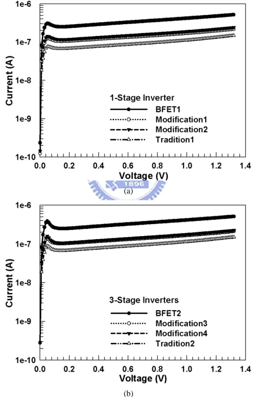
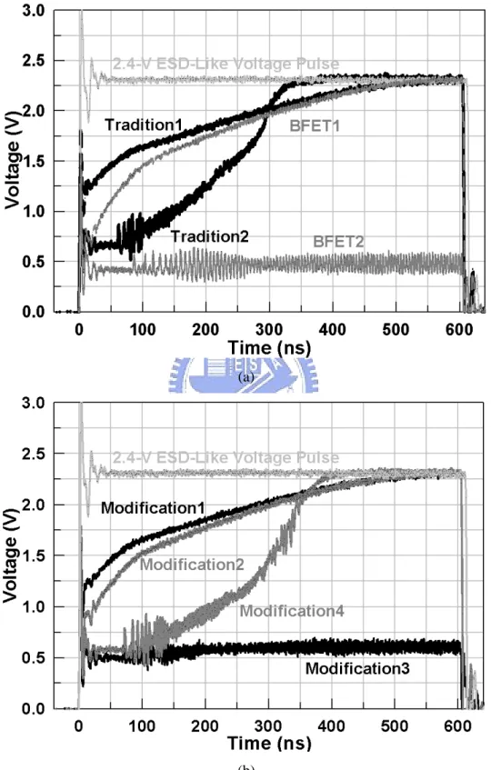
on its diffusions, and (b) the traditional layout style with the D of 2.0 μm and SB on its drain-side diffusions. 19 Fig. 2.2. DC leakage currents among the power-rail ESD clamp circuits of different designs with controlling circuit of (a) with 1-stage inverter and (b) 3-stage inverters. 21 Fig. 2.3. The measured voltage waveforms of (a) Tradition1, Tradition2, BFET1, and
BFET4, and of (b) Modification1, Modification2, Modification3, and Modification4, under 2.4-V ESD-like voltage pulses with 2-ns rise time. 23 Fig. 2.4. (a) The TLP I-V curves of Tradition1, Tradition2, BFET1, and BFET2. (b) The
zoomed-in view of (a) around the low-current region. 24 Fig. 2.5. (a) The TLP I-V curves of Modification1, Modification2, Modification3, and
Modification4. (b) The zoomed-in view of (a) around the low-current region. 25 Fig. 2.6. (a) The TLP I-V curves of Modification1, Modification2, Modification3, and
Modification4. (b) The zoomed-in view of (a) around the low-current region. 29 Fig. 2.7. The measured voltage waveforms of Modification1, Modification2, Modification3,
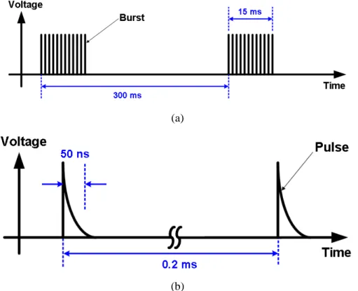
and Modification4 under the 1.2-V fast power-on condition with 100-ns rise time. 29 Fig. 2.8. Specified electrical fast transient (EFT) waveforms of (a) burst, and (b) single
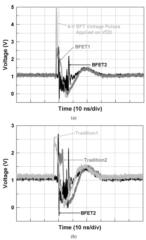
pulse, with a repetition frequency of 5 kHz. 31 Fig. 2.9. Measurement setup for electrical fast transient (EFT) test on the DUT with the VDD bias of 1.2 V. 31 Fig. 2.10. Under the 4-V EFT voltage pulse, the measured voltage waveforms of (a) BFET1 and BFET2, and (b) Tradition1 and Tradition2. 32 Fig. 2.11. Under the 9.5-V EFT voltage pulse, the measured voltage waveforms of (a)
BFET1 and BFET2, and (b) Tradition1 and Tradition2. 33 Fig. 2.12. Through the emission microscope with InGaAs FPA detector, (a) the abnormal
emission spots after the EFT test are located at the NMOS transistor of the second-stage inverter, the PMOS transistor of the third-stage inverter, and main ESD clamp NMOS transistor. (b) The zoomed-in view around the controlling circuit and the RC-based ESD-transient detection circuit. (c) The emission image is only located at the n-well resistance of the RC-based ESD-transient detection
Chapter 3
Fig. 3.1. Typical design scheme for NMOS-based power-rail ESD clamp circuit with an ESD-transient detection stage and controlling stage. 39 Fig. 3.2. Novel power-rail ESD clamp circuit with an new proposed ESD-transient detection circuit. This new proposed ESD-transient detection circuit is composed of an ultra small capacitor (C1), cascode NMOS transistors (Mnc1 and Mnc2), a resistor (R1), and a switch NMOS transistor (Mns). 40 Fig. 3.3. The comparison of the layout areas between the power-rail ESD clamp circuits
with (a) the traditional, and (b) the new proposed, ESD-transient detection circuits. 41 Fig. 3.4. The simulation result of the voltage potential on the gate terminal of main ESD clamp NMOS transistor in power-rail ESD clamp circuit. 42 Fig. 3.5. The measured voltage waveforms of power-rail ESD clamp circuits with the traditional and new proposed ESD-transient detection circuits under 5-V ESD-like voltage pulses with 2-ns rise time. 44 Fig. 3.6. The TLP I-V curves of the power-rail ESD clamp circuits with the traditional and the new proposed ESD-transient detection circuits. 45 Fig. 3.7. (a) The failure spot of the power-rail ESD clamp circuit with the traditional
ESD-transient detection circuit after 6.0-kV HBM ESD stresses. (b) Zoomed-in view of failure spot at Location A. 45 Fig. 3.8. The measured voltage waveforms of the power-rail ESD clamp circuits with the traditional and the new proposed ESD-transient detection circuits under the 1.2-V fast power-on conditions with (a) 100-ns rise time and (b) 2-ns rise time. 47 Fig. 3.9. Under the 10-V EFT voltage pulse, the measured voltage waveform of the
power-rail ESD clamp circuit with the new proposed ESD-transient detection circuit. 47
Chapter 4
Fig. 4.1. The traditional ESD protection design with the initial-off ESD protection device. (a) The ESD clamp device was kept off in normal circuit operation conditions. (b) During ESD stress, the ESD clamp device was triggered on to discharge ESD current. 50 Fig. 4.2. The new ESD protection concept with the initial-on ESD protection device. (a) The ESD clamp device was kept off in normal circuit operation conditions. (b)
The ESD clamp device was initially on when IC was floating. (c) The already-on ESD clamp device can rapidly discharge ESD current during ESD stress. 51 Fig. 4.3. The cross-sectional view of the initial-on SCR design with PMOS-triggered
technique. 52 Fig. 4.4. (a) The operation of the initial-on SCR design for power-rail ESD clamp circuit. (b) The equivalent circuit of the initial-on SCR design. The embedded PMOS transistor generates the trigger current to initiate the turn-on of SCR during ESD
stress. 53
Fig. 4.5. The top views of initial-on SCR devices with (a) structure-1 and (b) structure-2 layout styles realized in a 0.25-μm CMOS process. 54 Fig. 4.6. (a) The different gate-biased voltages were applied to the gate terminal of the
embedded PMOS transistor in the SCR structure. The measured DC I-V curves of the initial-on SCR devices with the layout styles of (b) structure-1, and (c) structure-2, under different gate-biased voltages. 55 Fig. 4.7. The DC I-V curves of the initial-on SCR devices with the layout styles of (a)
structure-1, and (b) structure-2, under different temperatures. (c) The dependence of SCR holding voltage on the temperature. 57 Fig. 4.8. (a) The measurement setup with ESD-like voltage pulse to investigate the turn-on efficiency of the LVTSCR and the PMOS-triggered SCR in structure-1 and structure-2 layout styles. The 6-V ESD-like voltage pulses were applied to the anodes of SCR devices with the rise time of (b) 10 ns and (c) 1.8 ns. (d) The
zoomed-in view on the clamped voltage waveform of (c) around the rising edge. 59
Fig. 4.9. (a) The TLP-measured I-V curves of the PMOS-triggered SCR device with structure-1 layout style under the embedded PMOS on or off. (b) The zoomed-in view of (a) around the low-current region. 61 Fig. 4.10. (a) The TLP-measured I-V curves of the PMOS-triggered SCR device with structure-2 layout style under the embedded PMOS on or off. (b) The zoomed-in view of (a) in the low-current region. 62 Fig. 4.11. (a) The on-chip ESD protection design for input, output, and power-rail ESD
clamp circuits with the initial-on SCR devices. (b) The initial-on SCR device can provide the low-impedance bi-direction discharging paths to discharge ESD currents during different ESD stress conditions. 64
Fig. 4.12. The ESD current discharging paths during the ESD stresses of (a) positive-to-VSS (PS) mode, (b) negative-to-VSS (NS) mode, (c) positive-to-VDD (PD) mode, and (d) negative-to-VDD (ND) mode. 65 Fig. 4.13. The ESD protection scheme realized with the initial-on SCR devices and ESD buses for the chip with separated power domains. 66
Chapter 5
Fig. 5.1. Cross-sectional views of (a) the PMOS-triggered SCR device with RC-based ESD transient detection circuit, and (b) the NMOS-triggered SCR device with RC-based ESD transient detection circuit and an inverter. 7 1 Fig. 5.2. Top views of (a) the PMOS-triggered, and (b) the NMOS-triggered, SCR devices
with three different channel lengths of 0.3 μm, 0.5 μm, and 0.75 μm in the embedded MOS transistor (original layout style). 72 Fig. 5.3. Top views of (a) the PMOS-triggered SCR device, and (b) NMOS-triggered SCR device, with merged layout style. Both anode-to-cathode spacings of PMOS-triggered and NMOS-triggered SCR devices are only 5.1 μm. 73 Fig. 5.4. The DC I-V curves of (a) the PMOS-triggered, and (b) the NMOS-triggered, SCR devices with three different channel lengths in the embedded MOS transistors (original layout style). 74 Fig. 5.5. The DC I-V curves of (a) the PMOS-triggered, and (b) the NMOS-triggered, SCR devices under two different layout styles. 75 Fig. 5.6. Under 5-V ESD-like voltage pulses with 2-ns rise time, the clamped voltage waveforms by (a) the PMOS-triggered SCR devices, and (b) the NMOS-triggered SCR devices, under three different channel lengths in the embedded MOS transistors (original layout style). 77 Fig. 5.7. (a) The TLP-measured I-V curves of the PMOS-triggered SCR devices with
different channel lengths and different layout styles in the embedded PMOS transistors. (b) The zoomed-in view of (a) around the low-current range. 78 Fig. 5.8. (a) The TLP-measured I-V curves of the NMOS-triggered SCR devices with
different channel lengths and different layout styles in the embedded NMOS transistors. (b) The zoomed-in view of (a) around the low-current range. 79 Fig. 5.9. (a) The failure spot is located at the embedded PMOS transistor in the
spots are located at the anode to embedded PMOS transistors in the PMOS-triggered SCR devices with 0.5-μm and 0.75-μm channel lengths. (d) The failure spot is located at the embedded NMOS transistor in the NMOS-triggered SCR device with 0.75-μm channel length. 82 Fig. 5.10. The turn-on mechanisms of (a) NMOS-triggered SCR device, and (b)
PMOS-triggered SCR device, under DC measurement with the embedded MOS transistors in off state. 83
Chapter 6
Fig. 6.1. The power-rail ESD clamp circuit can provide a low-impedance path between VDD and VSS to discharge the ESD current under the PS-mode and ND-mode ESD stresses. ESD current is discharged through the P-cell (N-cell) and power-rail ESD clamp device during PS-mode (ND-mode) ESD stress. 86 Fig. 6.2. The cross-section views of (a) gate-driven NMOS, (b) substrate-triggered FOD
(STFOD), and (c) substrate-triggered NMOS (STNMOS) with dummy gate. 88 Fig. 6.3. (a) The experimental setup to measure the turn-on efficiency of the power-rail
ESD clamp circuits. The measured voltage waveforms of the 3.3-V analog I/O pins on VDD node, which are clamped by (b) gate-driven NMOS, (c) substrate-triggered FOD, and (d) substrate-triggered NMOS with dummy gate, under ESD-like stress condition. 90 Fig. 6.4. The measured voltage waveforms of the 1.8-V analog I/O pins on VDD node,
which are clamped by (a) gate-driven NMOS, (b) substrate-triggered FOD, and (c) substrate-triggered NMOS with dummy gate, under ESD-like stress condition. 91 Fig. 6.5. (a) The failure spot is located at the GGNMOS in 1.8-V analog I/O pins with the MOS ESD protection design of AIO_2 after 0.5-kV PS-mode ESD stress. (b) The zoomed-in view of the failure spot. 95 Fig. 6.6. (a) The failure spot is located at the GGNMOS in 3.3-V analog I/O pin with the MOS ESD protection design of AIO_3 after 2.0-kV PS-mode ESD stress. (b) The failure spot is located at the GGNMOS in 3.3-V analog I/O pin with the MOS ESD protection design of AIO_2 after 0.5-kV PS-mode ESD stress. 96 Fig. 6.7. (a) The failure spot is located at the ESD clamp FOD in 1.8-V analog I/O pins
with the pure-diode ESD protection design of AIO_4 after 3.5-kV PS-mode ESD stress. (b) The zoomed-in view of the failure spot. 97
Fig. 6.8. (a) The failure spot is located at the ESD clamp FOD in 3.3-V analog I/O pins with the pure-diode ESD protection design of AIO_4 after 2.5-kV PS-mode ESD stress. (b) The zoomed-in view of the failure spot. 98 Fig. 6.9. (a) The failure spot is located at the GDPMOS in 1.8-V analog I/O pin with the MOS ESD protection design of AIO_1 after 3.0-kV ND-mode ESD stress. (b) The failure spot is located at the GDPMOS in 1.8-V analog I/O pin with the MOS ESD protection design of AIO_2 after 1.5-kV ND-mode ESD stress. 99 Fig. 6.10. (a) After 2.5-kV ND-mode ESD stress, the failure spot is located at the guard ring in AIO_4 of 1.8-V process. (b) The zoomed-in view of the failure spot at guard ring corner. 100 Fig. 6.11. (a) The parasitic npn bipolar transistor was constructed between the N+/PW diode and N+/NW guard ring. (b) The ESD current discharged through the parasitic npn bipolar transistor to grounded VDD during the ND-mode ESD stress causes the unexpected ESD failure. 101
Chapter 7
Fig. 7.1. ESD protection scheme in an IC product with separated power domains. The ESD protection circuits included input, output, and power-rail ESD clamp circuits. 104 Fig. 7.2. After ND-mode MM ESD stress on I/O pins, the I-V characteristics of
VDD2-to-VSS2 showed higher leakage currents than that before ESD stress. 105 Fig. 7.3. According to EMMI failure analysis, abnormal hot spots were found at the
interface circuits (see the circled areas) after ND-mode MM ESD stress on (a) Pin-A, and (b) Pin-B. (c) The corresponding layout locations of the interface circuits were indicated the failure spots in (a) and (b). 106 Fig. 7.4. After ND-mode MM ESD stress on Pin-A, the failure spots were located at (a)
PMOS transistor (M1), and (b) the other PMOS transistor (M2). 107 Fig. 7.5. The ESD current could be discharged through the circuitous path to cause ESD
damages to M1 and M2 during ND-mode MM ESD stress on Pin-A. 107 Fig. 7.6. (a) NMOS transistor (Mb), and (b) PMOS transistor (M3) of the interface circuits were destroyed after ND-mode MM ESD stress on Pin-B. 108 Fig. 7.7. ESD discharging paths during ND-mode MM ESD stress on Pin-B. The Mb and M3 were damaged after such ESD stress. 108 Fig. 7.8. The proposed ESD protection solution to rescue ESD failures at the interface
Fig. 7.9. The estimations of the induced voltage potential under the cross-power-domain (a) VDD1-to-VDD2, and (b) VDD1-to-VSS2, ESD stresses. 111 Fig. 7.10. The ESD protection design with resistor-diode clamp had been proposed to
protect the interface circuits between separated power domains [40]. 112 Fig. 7.11. The ESD protection design with (a) a special driver and (b) a special receiver for interface circuits between separated power domains [41]. 113 Fig. 7.12. The ESD protection design with grounded-current-trigger (GCT) NMOS transistor for interface circuits between separated power domains [42]. 114 Fig. 7.13. A proposed cross-power-domain ESD protection design with gate-controlled
PMOS and NMOS (GC-PMOS and GC-NMOS) transistors and source pumping
mechanism. 116
Fig. 7.14. The cross-power-domain ESD protection design with GCT NMOS and GC-NMOS transistors and source pumping mechanism. 117 Fig. 7.15. (a) The 100-ns TLP measured I-V characteristics of the cross-power-domain ESD protection design with GC-PMOS and GC-NMOS transistors under VDD1-to-VSS1, VSS1-to-VSS2, and VSS2-to-VDD2 three different stress combinations. (b) The 100-ns TLP measured I-V characteristics of the three different cross-power-domain ESD protection designs under VDD1-to-VSS2
stresses. 119
Fig. 7.16. The influence of source pumping mechanism on the TLP measured I-V characteristics of the cross-power-domain ESD protection designs under VDD1-to-VSS2 stresses. (a) With or without source pumping resistance in the design with GCT NMOS transistor. (b) With source pumping resistance of 5 Ω or 15 Ω in the design with GC-PMOS and GC-NMOS transistors. 120 Fig. 7.17. (a) After VDD1-to-VSS2 HBM ESD stress, the failure spots of the
cross-power-domain ESD protection design with diodes were located at the source side of the driver’s PMOS transistor (Mp1). (b) The zoomed-in view of the failure spot. (c) The failure mechanism of the cross-power-domain ESD protection design with diodes under VDD1-toVSS2 HBM ESD stress. 122 Fig. 7.18. ( a ) A f t e r V D D 1 - t o - V S S 2 H B M E S D s t r e s s , t h e f a i l u r e s p o t s o f
cross-power-domain ESD protection design with GC-PMOS and GC-NMOS transistors were located at the driver’s PMOS transistor (Mp1). (b) The zoomed-in view of the failure spot. 123
Fig. 7.19. (a) and (b), both cross-power-domain ESD protection designs with diodes and GC-PMOS and GC-NMOS transistors have the failure spots at the driver’s PMOS transistor (Mp1) after VDD1-to-VDD2 ESD stresses. (c) The other failure spots of cross-power-domain ESD protection designs with diodes were found at the receiver’s PMOS transistor (Mp2) after VDD1-to-VDD2 MM ESD stress. 124
Chapter 1
Introduction
In this chapter, the background and the organization of this dissertation are discussed. First, the main concerns of electrostatic discharge (ESD) protection design for integrated circuits in deep-submicron and nanoscale complementary metal-oxide-semiconductor (CMOS) processes are introduced. Secondly, the ESD protection design for analog input/output (I/O) interface circuits and the cross-power-domain ESD issues of CMOS integrated circuit (IC) products with multiple separated power domains are discussed. Finally, the organization of this dissertation is described.
1.1. Background of ESD Protection Design for Integrated
Circuits in Advanced CMOS Technologies
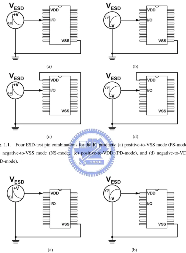
With the continuous evolution of CMOS technology, electrostatic discharge (ESD) protection has become a tough task on the product reliability of CMOS integrated circuits. The scaled down device dimension with thinner gate oxide and shallower junction depth in nanoscale CMOS technology is easily damaged by ESD stress. The ESD specification of commercial IC products are generally required to be higher than 2 kV in human-body-model (HBM) [1] and 200 V in machine-model (MM) [2] ESD stresses. The ESD-test pin combinations are shown in Fig. 1.1. ESD stresses may have positive or negative voltages on an I/O pin with respect to the grounded VDD or VSS pin. For comprehensive ESD verification, the VDD-to-VSS ESD stresses and pin-to-pin ESD stresses had also been specified to verify the whole-chip ESD robustness, which are shown in Fig. 1.2 and 1.3, respectively. Therefore, on-chip ESD protection circuits must be added into CMOS ICs to achieve the required ESD robustness [3]-[5]. A typical design of on-chip ESD protection circuits is illustrated in Fig. 1.4. The power-rail ESD clamp circuit is an efficient design to achieve whole-chip ESD protection in IC products [6], [7]. It not only can enhance ESD robustness of VDD-to-VSS ESD stress, but also can significantly improve ESD robustness of the ESD stresses between input/output and VDD/VSS [7].
(a) (b)
(c) (d)
Fig. 1.1. Four ESD-test pin combinations for the IC products: (a) positive-to-VSS mode (PS-mode), (b) negative-to-VSS mode (NS-mode), (c) positive-to-VDD (PD-mode), and (d) negative-to-VDD (ND-mode).
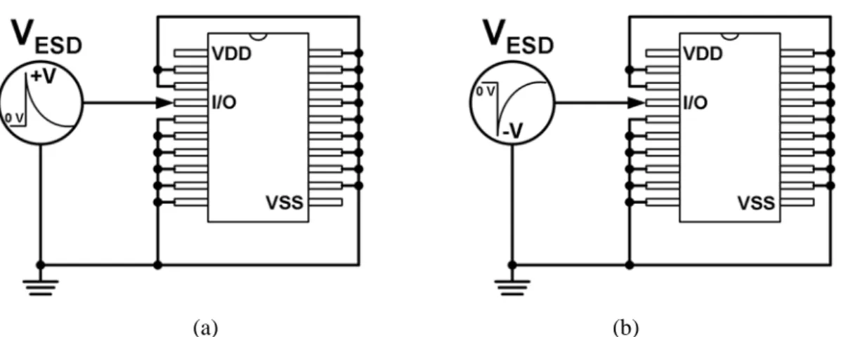
(a) (b)
(a) (b)
Fig. 1.3. Pin combinations in pin-to-pin ESD tests: (a) positive mode, and (b) negative mode.
Fig. 1.4. Typical on-chip ESD protection circuits for CMOS ICs.
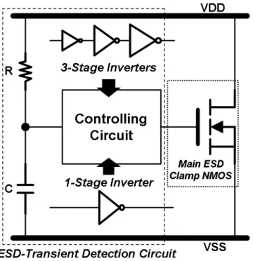
In general, the power-rail ESD clamp circuit consists of an ESD-transient detection circuit, a controlling circuit, and a main ESD clamp devices, as shown in Fig. 1.5. The ESD-transient detection circuit, which is usually implemented by resistor-capacitor (RC) network, is used to distinguish ESD-stress conditions from normal circuit operation conditions due to the difference in the rise time between these two conditions [6], [7]. Then, the controlling circuit implemented by single- or multi-stage inverters cooperates with the RC-based ESD-transient detection circuit to command the main ESD clamp device into the on state or the off state under the ESD-stress conditions and normal circuit operation conditions. The main ESD clamp device is always required to provide a low impedance discharging path under ESD-stress conditions, while it must be kept off under normal circuit operation conditions. NMOS transistors have been widely used as the main ESD clamp device to obtain the desired ESD protection capability.
Fig. 1.5. Typical design scheme for NMOS-based power-rail ESD clamp circuit with RC-based ESD-transient detection circuit.
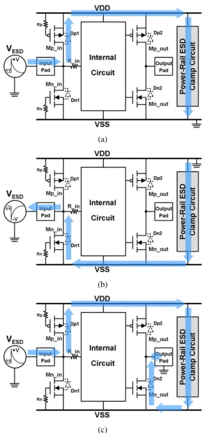
During the positive-to-VDD (PD) mode and negative-to-VSS (NS) mode ESD stresses, ESD current is discharged through the forward-biased Dp1 and Dn1, which are parasitic diodes in gate-VDD PMOS (GD-PMOS) transistor, Mp_in, and gate-grounded NMOS (GG-NMOS) transistor, Mn_in, respectively. To avoid the GD-PMOS and GG-NMOS from being operated under breakdown condition during the positive-to-VSS (PS) mode and negative-to-VDD (ND) mode ESD stresses, which results in a substantially lower ESD robustness, the power-rail ESD clamp circuit is used between VDD and VSS to provide ESD current paths between the power rails [7]. Thus, ESD current is discharged from the I/O pad through the parasitic forward-biased Dp1 in Mp_in to VDD, and discharged to the grounded VSS pin through the turned-on power-rail ESD clamp circuit during PS-mode ESD stresses, as shown in Fig. 1.6(a). Similarly, ESD current is discharged from the VDD pin through the turned-on power-rail ESD clamp circuit and the parasitic forward-biased Dn1 in Mn_in to the I/O pad during ND-mode ESD stresses, as shown in Fig. 1.6(b). Under VDD-to-VSS ESD tests, ESD current flows through the power-rail ESD clamp circuit between VDD and VSS. During pin-to-pin ESD stresses, ESD current flows from the zapped I/O pad through the parasitic forward-biased Dp1 in Mp_in, the turned-on power-rail ESD clamp circuit, and the parasitic forward-biased Dn2 in Mn_out to the grounded I/O pad, as shown in Fig. 1.6(c). With the turn-on efficient power-rail ESD clamp circuit, ESD current can be discharged by
the parasitic forward-biased diodes in GD-PMOS and GG-NMOS transistor to obtain the higher ESD robustness under all ESD test modes.
(a)
(b)
(c)
Fig. 1.6. ESD current paths in the typical double-diode ESD protection scheme under (a) PS-mode ESD stresses, (b) ND-mode ESD stresses, and (c) pin-to-pin ESD stresses.
To efficiently protect the core circuits realized with much thinner gate oxide in nanoscale CMOS technology, some studies had reported the efficient power-rail ESD clamp circuits with modified circuit designs [8]-[11]. All of them were based on the power-rail ESD clamp circuits with gate-driven mechanism which was basically implemented by the RC-based ESD-transient detection circuit with a controlling circuit [6]-[11], as illustrated in Fig. 1.5. Besides, those previous works also adopted the power-rail ESD clamp NMOS transistor with no snapback operations to obtain excellent turn-on efficiency. The snapback phenomenon usually occurs in NMOS transistors, npn bipolar transistors, or silicon controlled rectifiers (SCRs) under higher voltage and current stress conditions. No snapback means that the huge ESD current was discharged by the channel current of NMOS transistors. Therefore, those NMOS transistors in the power-rail ESD clamp circuits were traditionally drawn with huge channel width of several-thousand micrometer to achieve the required ESD robustness under no snapback operation. They were often called as Big FET (BFET) in some previous literatures [8]-[11]. 3-stage inverters, which were adopted as a function of tapered buffer [12]-[16], usually performed the controlling circuit to efficiently turn-on or turn-off the BFET, which has large capacitive load from the NMOS transistor with a huge channel width in power-rail ESD clamp circuit. The tapered buffers, which are the multiple inverter stages with cascaded arrangement, are constantly applied to drive the large loading capacitance under a desirable propagation delay and power consumption [12]-[14]. However, such design concerns are not always appropriate to the function of the controlling circuits in the power-rail ESD clamp circuits because of two main reasons. First, the controlling circuits are only required to propagate a unity signal, such as logical high or logical low, in order to turn on the main ESD clamp devices under ESD-stress conditions, but they are not required to propagate a dynamic signal or alternating logic under normal circuit operation conditions. Second, the controlling circuits are always biased at the static off state under the normal circuit operation conditions in the power-rail ESD clamp circuits. Some basic circuit performances, such as short-circuit dissipation and propagation delay, would not be improved by the controlling circuits with the tapered buffer arrangement. Therefore, the controlling circuits with tapered buffer concepts should be unnecessary and even be unsuitable for power-rail ESD clamp circuits.
In addition, based on the traditional RC-based ESD-transient detection circuit [6], [7], the RC-time constant which is the product of the resistance (R) and capacitance (C) essentially dominated the turn-on duration of the main ESD clamp NMOS transistor. Therefore, the RC-time constant of the RC-based ESD-transient detection circuit should be
designed to sufficiently achieve a desirable turned-on duration of the main ESD clamp NMOS transistor. In general, the turn-on duration was adjusted to meet the period of human-body-model (HBM) ESD event, which is about several hundred nano-seconds (ns) [1]. The extended RC-time constant not only accompanies with the larger layout sizes of the resistance and capacitance, but also is subject to mis-trigger the main ESD clamp NMOS transistor under fast power-on applications [10]. Several previous works proposed special circuit schemes with feedback circuit techniques to extend the turn-on duration under a small RC-time constant [9], [10], [17]-[19]. However, those feedback circuit designs always suffered from the latch-on threats under the fast power-on events or the electrical fast transient noise [20], [21]. Besides, other circuit schemes without feedback circuit techniques, such as on-time control circuit [9] and multi-RC-triggered [11], also had been presented to achieve the desirable turn-on duration and to avoid the latch-on threat. But, extra resistors and capacitors have to be implanted into these designs, which occupying a quite silicon area. In summary, the circuit scheme of controlling circuit and ESD-transient detection circuit should be optimized to obtain more efficient and reliable power-rail ESD clamp circuit in nanoscale CMOS technology.
1.1.2. Issue of SCR Device as Main ESD Clamp Device
In IC products, the on-chip ESD protection designs are required to provide higher ESD robustness with smaller layout area to save the chip area. Silicon controlled rectifiers (SCRs) have been used as on-chip ESD protection devices, because of their superior area-efficient ESD robustness [22]. However, SCR has some drawbacks, such as higher trigger voltage (Vt1), lower turn-on efficiency, and even latchup danger. The traditional I-V characteristic of the SCR device is shown in Fig. 1.7. The higher trigger voltage and lower turn-on efficiency would not efficiently protect the internal circuits in deep-submicron or deep-submicron CMOS technology. Therefore, the low-voltage-triggered SCR (LVTSCR) was invented to reduce the trigger voltage of SCR device [23]. Moreover, some advanced circuit techniques (the gate-coupled [24], substrate-triggered [25], and GGNMOS-triggered [26] techniques) were also reported to enhance the turn-on efficiency of SCR devices. However, those modified SCR designs [23]-[26] still function as the initial-off ESD devices. Recently, in order to further enhance the turn-on speed, the native-NMOS-triggered SCR (NANSCR) has been reported to achieve more efficient ESD protection for CMOS ICs in a 0.13-μm CMOS technology [27]. In this NANSCR, it uses the special native device to achieve the “initial-on”
function. The native device is the NMOS transistor with the almost zero threshold voltage (about 0.1 V). It is directly built in a lightly-doped p-substrate, whereas the normal NMOS is in a heavily-doped p-well in p-substrate CMOS technology. Besides, to keep such NANSCR in off state when the IC is in normal operation, it needs the on-chip negative-bias generator [28]. Such extra efforts to realize the NANSCR with negative gate bias for on-chip ESD protection design would cause some limitation in practical applications of general CMOS ICs. On the other hand, the lower holding voltages (lower than VDD operation voltage) could cause latchup triggering by external noise pulses during normal circuit operation conditions. Several previous studies had been presented to increase the holding voltage during normal circuit operation conditions, such as dynamic holding voltage SCR (DHVSCR) [29], SCR devices with stacked diode string [25], and stacked SCR devices [30]. In addition, the high-current-triggered SCR devices had been proposed to safely protect the internal circuits without being accidentally triggered on by the electrical noisy pulse during normal circuit operation conditions [31]. SCR device is susceptible to latchup danger, especially in the application of power-rail ESD clamp circuit. However, with the scale-down device dimension in nanoscale CMOS technology, the VDD operation voltage is also scaled down in order to meet the circuit requirement and gate-oxide reliability. If the holding voltage of the SCR device is greater than the VDD operation voltage, latchup issue will not occur in such IC products with nanoscale CMOS technology. Therefore, the SCR device can be more safely and widely to use as power-rail ESD clamp circuit in nanoscale CMOS technology.
Voltage (V) C u rre n t (A ) Holding Point Trigger Point V DD V o lta g e In terna l C ircui t B rea kdow n V o lta g e (G at e O xi d e Br e ak d o w n V o lt ag e ) ESD Protection Design Window Internal Circuits Destruction L at chu p I ssu e Ron 0
Fig. 1.7. The design window for ESD protection. The traditional I-V characteristic of SCR device can not meet to this ESD protection design window.
1.2. ESD Issues in Analog I/O and Multiple Separated Power
Domains Interface Circuits
A conventional ESD protection design for the digital input pin is also shown in Fig. 1.4. The gate-grounded NMOS (GGNMOS) and gate-VDD PMOS (GDPMOS) are often designed with a large device dimension and a wider drain-contact-to-poly-gate layout spacing to sustain the desired ESD level, typically 2 kV in HBM and 200 V in MM ESD stresses. The resistor R in the digital input ESD protection circuit is usually included to effectively protect the gate oxide of input stage. However, the series resistance between the input pad and input stage is forbidden for current-mode input signals or high-frequency applications. Furthermore, the series resistance and the large junction capacitance of the ESD clamp devices cause a long RC delay to the input signals; therefore, such ESD protection circuit is not suitable for analog I/O interface circuits [32]. A typical ESD protection design for analog I/O interface circuit has been reported, as shown in Fig. 1.8. In order to reduce the input capacitance of the analog I/O interface circuits, the N-cell and P-cell are both designed with smaller device dimensions. However, such small devices can’t sustain high enough ESD level, while the analog pin is zapped in the positive-to-VSS (PS-mode) or the negative-to-VDD (ND-mode) ESD stress (the devices operated in the breakdown condition). Therefore, a turn-on efficient power-rail ESD clamp circuit between VDD and VSS was co-constructed into the analog ESD protection circuit to improve the overall ESD level of the analog I/O interface circuits.
Fig. 1.8. The ESD protection circuit for analog I/O pin. The protection circuit includes the P-cell, N-cell, and power rail ESD clamp circuit.
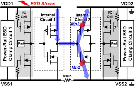
In addition, as the ultra-large-scale-integrated (ULSI) circuits being continually developed toward system-on-chip (SoC) applications, more and more multiple separated power domains are used in a SoC IC for specified circuit functions, such as digital/analog circuit blocks, mixed-voltage circuit blocks, and power management considerations, as shown in Fig. 1.9. However, the IC products with multiple separated power domains often have more unexpected current paths during ESD stresses and easily cause damages across interface circuits between different power domains beyond the ESD protection circuits of I/O cells [33]-[37], as presented in Fig. 1.10. Such ESD failures across interface circuits between different power domains are often difficult to be clearly examined and revised, even with a lot of failure analysis procedures. Several cross-power-domain ESD protection designs had been studied and proposed to avoid ESD damages on the interface circuits between two separated power domains [33]-[38]. The bi-directional diode connection had been generally used to connect the separated power or ground pins in different power domains, as shown in Fig. 1.11. The bi-directional diode connection can construct the completely whole-chip ESD current discharging paths under cross-power-domain ESD stresses [39], [40]. According to the previous studies [40]-[42], the overstress voltages across the interface circuits between separated power domains easily caused the ESD damages, such as gate oxide damage, junction filament, and contact destroy under cross-power-domain ESD stresses.
Fig. 1.9. The integrated circuits are continually developed toward system-on-chip (SoC) applications. Multiple separated power domains are used in a SoC IC for specified circuit functions.
Fig. 1.10. Interface circuits across separated power domains are easily damaged under cross-power-domain ESD stresses.
Fig. 1.11. Bi-directional diode connection had been generally used to connect the separated power or ground pins in different power domains.
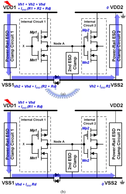
When the ESD voltage was applied on the VDD1 and grounded VDD2 under the cross-power-domain ESD stresses, the ESD current can be discharged from the VDD1 to the VSS1 by the power-rail ESD clamp circuit 1 in the power domain one, from the VSS1 to the VSS2 through the inserted bi-directional diode connection, and then from the VSS2 to the grounded VDD2 through the other power-rail ESD clamp circuit 2 in the power domain two, as the discharged path shown by dashed line in Fig. 1.12(a). The Vh1 and Vh2 are the holding voltage of the power-rail ESD clamp circuits 1 and 2, respectively. Then, the Vhd is the holding voltage of the bi-directional diode connection between the separated power domains.
Among the parameters, the R1, R2, and Rd are the turn-on resistances of the power-rail ESD clamp circuits 1, 2, and the bi-directional diode connection, respectively. When the ESD current was conducted by this long discharging path, it would induce the overstress voltage across the each MOS transistor in interface circuits between separated power domains [40]-[42]. The induced voltage drops with discharging ESD currents from VDD1 to VDD2 on each node of the interface circuit had been estimated, as shown in Fig. 1.12(a).
(a)
(b)
Fig. 1.12. The estimations of the induced voltage potential under the cross-power-domain (a) VDD1-to-VDD2, and (b) VDD1-to-VSS2, ESD stresses.
The voltage potential at node A could be raised up to the VDD1 because the driver’s PMOS transistor (Mp1) had an initially floating gate situation. The highest voltage drop was applied across the gate oxide of the receiver’s PMOS transistor (Mp2) in interface circuits under the VDD1 to VDD2 ESD stresses. On the other hand, the highest voltage drop was also generated across the gate oxide of the receiver’s NMOS transistor (Mn2) in interface circuits under the VDD1 to VSS2 ESD stresses. The similar estimation on voltage drops during ESD stress was presented in Fig. 1.12(b). As the CMOS technologies being continually shrunk toward nanometer scales, the breakdown voltages of ultra-thin gate oxide in the MOS transistors were sharply reduced to impact the ESD protection designs. It was important to avoid the gate oxide damages of the MOS transistors in the interface circuits by ESD-current induced overstress voltages. Therefore, the second ESD clamp (2nd ESD clamp) designs had been applied to reduce the overstress voltages across the interface circuits, as shown in Figs. 1.12(a) and 1.12(b). Furthermore, the 2nd ESD clamp with desired trigger mechanism [38], [40]-[42] also had been proposed to rapidly and efficiently clamp the overstress voltages across the interface circuits between separated power domains, especially in the integrated circuits with nanoscale CMOS technology.
1.3. Organization of This Dissertation
To overcome the challenges in ESD protection design for power-rail ESD clamp circuits, analog I/O interface circuits, and cross-power-domain interface circuits in deep-submicron and nanoscale CMOS integrated circuits, several new designs are developed and verified in this dissertation. This dissertation comprises eight chapters. In Chapter 2, the comparison of the controlling circuit implemented with 1-stage or 3-stage inverters has been presented [43]. Then, the drain-contact-to-poly-gate spacing (D) of the main ESD clamp NMOS transistor has been also split in order to investigate the influence of this spacing on the ESD protection capability. In Chapter 3, an efficient ESD-transient detection circuit with capacitance coupling mechanism has been proposed to accomplish the desirable function on commanding the main ESD clamp NMOS transistor. A novel initial-on SCR design is proposed to achieve the lowest trigger voltage and the highest turn-on efficiency of SCR device in Chapter 4. Chapter 5 further discusses optimizations on the initial-on SCR devices are presented [44]-[46]. The modified initial-on SCR device with merged layout style is also proposed to enhance its ESD protection capability. Besides ESD protection design for power-rail ESD clamp circuit, the comparison among different ESD protection designs for analog I/O